Identifying and avoiding fake electronic components on PCB is crucial for ensuring the reliability and performance of your electronics. But with the development of electronics, the replacement cycle of various electronic components, including plastic integrated circuits, is getting shortage in resourcing, which brings the big difficulties to the component management supply chain.
For some components has been updated and may no longer to produced, especially for equipment manufacturers with small components consumption, many varieties and high reliability requirements. Due to small procurement volume, they often cannot be purchased directly from originally manufacturers and much be purchased through agents, thus proving the opportunities for fake components to enter the market. Herein, Best team would like to share some information about definition of fake components and methods to verify & identify fake parts, hope this is helpful for everyone that has demands on components.

What Are Fake Components and How Does It Affect Industry?
Fake components, also known as counterfeit electronic components, are parts that are misrepresented by sellers as genuine, but are actually inferior in quality and may not meet the specifications of the original manufacturer. The U.S. Department of Energy /SAE AS5553 defines counterfeit components as copies or substitutes produced without legal authorization, or components whose materials, properties, or specifications are falsely advertised. These components can be refurbished parts, parts with altered date codes or markings, or completely fabricated units that mimic real products. They are introduced into the supply chain through various illegal means, including unauthorized factories and distributors.
Counterfeiting is a violation of the legal rights of intellectual property owners. The economic cost of counterfeit components far exceeds the cost of replacement, including safety costs, lost performance, repair or replacement, and important is reputational impact. For example, a $2 component used on a printed circuit board (PCB) can cost up to $20 to replace once it is detected to be a counterfeit component. More importantly, counterfeit components have the potential to cause serious consequences. A case in point is the crash of a chartered Convair580 near the Danish coast on September 8th, 1989. In addition, counterfeit goods may be used in some sabotages, which is likely to pose a serious challenge to national security. Therefore, identifying counterfeit components at the initial stage appear to be particularly important during the initial stage, especially before the PCBA assembly process.
How to Identifying Fake Electronics Components at Initial Stage?
At present, the fake integrated circuits on the market can be divided into refurbished integrated circuits and counterfeit integrated circuits. The mass entry of fake and inferior devices into the market or the supply chain of military products has seriously affected the quality and reliability of our country’s equipment products. Here are some methods to confirm whether you are using a counterfeit component.
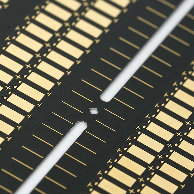
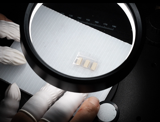
- Visual inspection
There will be polished marks or traces on the surface of fake electronic components, and some sellers will apply a thin film on the surface of fake electronic components, so that people cannot see the polishing marks. This kind of smearing fake electronic components look brighter than the genuine one. In addition, observing the edge of electronic components also is a good way, due to the polishing process, refurbished electronic components are easily changed to right angles from rounded corners. So, if you see that the edge of electronic components is a “Right Angle”, then you can think that it is refurbished goods!
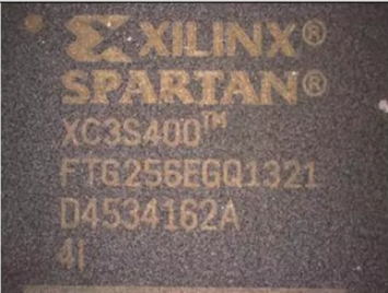
- Silkscreen or texts on surface
To ensure the high-quality of products, most of chips use laser printing or marking technology with a dedicated printer to print silkscreen or text. By this method, its silkscreen is clear, neither conspicuous, nor fuzzy and difficult to erase. But the refurbished chip either has a “jagged” feeling because the writing edge is corroded by the cleaning agent, or the printing is fuzzy, different in depth, wrong in position, easy to erase or too conspicuous. During the verifying process, acetone can be used to wipe the silkscreen as well to confirm whether it is remark part.
- Pin-legs on the chips
The pins of genuine parts always in silver powder with darker and uniform color, and they are not easy to have oxidation traces. If it is a refurbished electronic component, then its pin is generally tinned and brighter like a new one. In addition, DIP parts and other plug-ins should not have scratched pins, even if there is scratch should be neat and the metal exposure is clean and no oxidation.
- Documentation and traceability
Genuine parts will have proper documentation including batch numbers, date codes, and traceability. And the labels of the genuine parts including the labels on the bottom side of the chip, should be consistent and the date code should be consistent with the device product, while the labels of the refurbished pieces without Remark are confused and the production date is different. Verify these details with the manufacturer’s records if possible.
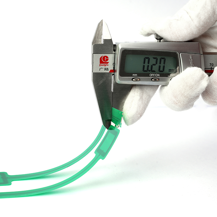
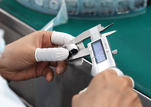
- Thickness measurement
Because of the silkscreen on the electronic components, if you want to refurbish it is must to be polished, which will affect the thickness of electronic components. If you are a layman in electronic components industry, it is easy to ignore this.
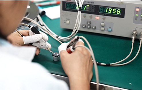
- Function test
Conduct electrical testing to verify that components meet the specifications claimed. This can include check if the electronic parameters align with what’s expected from the datasheet.
Above are the measurements about how to identify the fake components, however, last but not important is looking for a reliable reputable distributor or buy from original manufacturers directly. These sources are less likely to stock counterfeit parts. Best Technology not only provides PCB & PCBA assembly services, but also offers components sourcing and purchasing from original manufacturers. If you are looking for a reliable supplier, welcome to contact with us or send e-mail to us.