Archive for March, 2016

What’s the counterbore and countersink?

Saturday, March 26th, 2016

Somebody may not know the different between counterbore and countersink on PCB.

Both are used to mount nails to keep the PCB in the suitble position.

The cross-section of the counterbore looks like letter “T”, but the countersink looks like a funnel.

Pls see the below picture:

PCB counterbore

PCB counterbore

PCB countersink

PCB countersink

Pls visit our website if you have more questions about PCB.

You may also like

What’s Single Layer PCB?

Friday, March 25th, 2016

Normally PCB which only one conductor is single layer PCB. Common conductor are copper , AgPd (Silver Palladium) AuPd (Gold Palladium ), Al(aluminum). Normally, for FR4 PCB, metal core PCB and Flexible PCB, the conductor are copper. For ceramic PCB, the conductor can be copper, AgPd and Aupd. Here some common structures for your reference.

single side FR4 PCB

single side FR4 PCB

single side ceramic PCB

single side ceramic PCB

Of course, there are some special circumstances, even only one conductor, but they are not single layer PCB, they are named Dual Access PCB.
For example:

dual access FR4 PCB

dual access FR4 PCB


You may also like

MCPCB can be without solder mask?

Friday, March 25th, 2016

MCPCB can be without solder mask

Yes, we can make the MCPCB without solder mask! How to do MCPCB without solder mask?


  • First step, we use our dielectric layer and laminate with copper, so we get the material of this stack up

Top: copper foil

Middle: dielectric layer

Bottom: Aluminum or Copper or Iron substrate


  • Second step, etch copper to get the trace, the areas without trace will expose the dielectric layer, the color of 1W/m.K & 2W/m.K raw material is white, 3W/m.K is light blue.


3 w m/k dielectric layer is light blue

3 w m/k dielectric layer is light blue

2 w m/k dielectric layer is white

2 w m/k dielectric layer is white

  • Third step, do the surface finish, HAL-LF, OSP, ENIG, etc…,here you will kow for no Soldermask ,it have to do surface finishing for all circuits,so if you would like to protect parts of circuits layer and which don’t need do surface finishing.

MCPCB without solder mask have no bad influent the function of the board, so solder mask with or without, only depends on your requirement.please visit for metal core PCB if you would like to know more.

You may also like

What’s the halogen-free copper clad materials

Friday, March 25th, 2016

According to the JPCA – ES – 01-2003 standard: chlorine (C1), bromine (Br) is less than 0.09% Wt (weight ratio) of the copper clad, defined as halogen-free copper clad. (at the same time, the CI + Br total less than 0.15%  [1500 parts per million])  Most of the halogen free materials are mainly composed of phosphorus and phosphorus nitrogen.when the phosphorus resin burning, it will thermal decomposition by heating and generate partial poly phosphoric acid,the partial poly phosphoric acid have strong dehydration property to come into being the carbon film on the surface of the high polymer resin,to insulated resin burning surface is exposed to air, that the fire is extinguished, flame retardant effect.

You may also like

What’s the meaning for S/M in PCB?

Friday, March 25th, 2016

S/M means solder mask, it is a kind of the Liquid photosensitive ink, it is the green, yellow, red, black or white color on PCB surface. We print solder mask on the PCB surface that no need soldering, and then drying and curing.

With solder mask, the Tin won’t stick to the PCB.

You may also like

The advantage and disadvantage of aluminum PCB

Friday, March 18th, 2016

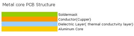
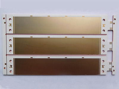
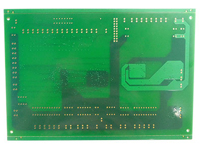
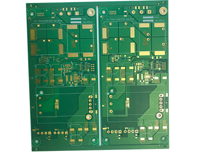
The aluminum PCB is a unique metal base copper clad laminate , it has good thermal conductivity, electrical insulation properties and machining property.

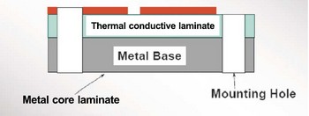
The structure of aluminum PCB is divided into three layers.

First layer: base layer, it is the metal substrate, which can choose copper or aluminum.

Second layer: dielectric Layer, its thickness be from 0.003 inch to 0.006 inch.

Third layer: circuit layer, the copper thickness of the circuit is from 1oz to 10oz.

The advantage of aluminum PCB:

  • it has good heat radiation and better strength.


The disadvantage of aluminum PCB:

  • High cost.
  • The current mainstream can only do single aluminum PCB, it is difficult to do double sided aluminum PCB.
  • The product will be more easily to have matter in electrical strength and pressure.

Aluminum core PCB have good thermal conductivity but Ceramic PCB will better,if you would like to know more about the different from FR4,MCPCB and Ceramic PCB,pls visit to for more information.


You may also like

Join US – Best Technology Co, Limited

Thursday, March 3rd, 2016

As Best Tech get older and bigger,more worker and staff are needed,but we would better to employ worker who work in production line from China.For the staff in salesDepartment,we also would like to get some colleagues from worldwide,so now pls see the information as below to know who we would like:

Sales Manager:

  • Three years above experience in sale,2 years experience in Director of the ministry of foreign trade. Experienced with PCB or electronic is prefered.
  • Develop customers independently, customer management and Excellent customer analysis and business negotiation skills.
  • Manage Foreign trade team and Lead the group to complete performance targets.
  • College degree or above,CET-6 or above(For Chinese)
  • Fluent English:Can communicate with foreign session skilled, face to face to carry out business activities.

Salesman:

  • Responsible For Developing Customers
  • Maintain old customers
  • Search and find new customers from Google,B2B and yellow page,etc
  • Communicate with customers by telephone and email. Good business letter writing skills or the strong basic professional knowledge required meanwhile excellent verbal is required to be able to talk with customers by telephone and face to face without any problem
  • One year above working experience. Professional and academic: Business English, international trade,Marketing,etc, college degree or above; Secondary students will be fine if outstanding ability.
  • Ladies First,age:18~35; Excellent fresh graduate can also be considered
  • Experience in PCB/FPC sales or Understanding PCB production process will be better
  • No required for the experience in L/C, Trade documents and shipping management.Our payment is T/T and Net 30 days.

Company information:

  • Name:Best Technology Co, Limited
  • Address:Working place: 9E, Jindacheng Building, Center Rd(CBD of ShaJing), Shajing Town, Bao’an District, Shenzhen,China
  • Working Time:Monday ~Friday:08:30~12:00a.m,14:00~18:00 p.m; Saturday:09:00~12:00a.m;
  • Benefits:High basic salary+ push money+ year end bonus+ Full Attendance Award(High to 6200 Yuan/year);in-house and off-site training;Development :salesman- Supervisor -manager-director- vice president;International or Domestic Travel Incentives;free dinner and have lunch with boss + afternoon tea: Snacks and fruits;Free 1-layer check-up;Spring Festival transportation costs for Expenses(For Chinese);Paid annual leave:5 days for working than one year,and increasing every year;Sports fitness leisure activities every week, every month large group activities (camping, the beach barbecue), enterprise Internet activities every quarter, 1 ~ 2 times a year to expand training;Provide free accommodation;
  • Products:Metal PCB,Ceramic PCB,HDI PCB,RF PCB,SMT stencil and so on.

You can visit our website for more information or send your resume into info@bestpcbs.com,also send us your email if you would like to know more.

You may also like