Archive for January, 2019

3 Steps to Recycle PCB

Friday, January 25th, 2019

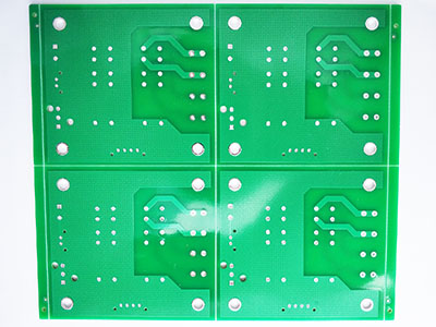
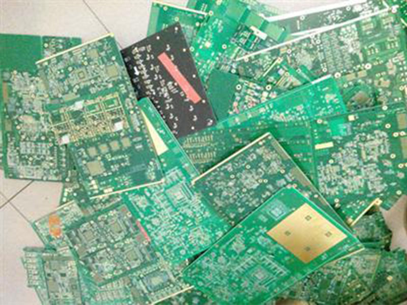
Everything will break if it has been operated for a long time, especially electronic products. However, the broken items, which can be recycled, are not completely waste, and the printed circuit board is the same. With the development of technology, the amount of electronic products increase rapidly. Their operating cycles are shortening and many products are discarded without damage, resulting in serious waste. Meanwhile, there are some substances of electronics will d harms to the environment. Therefore, it is required to recycle them.

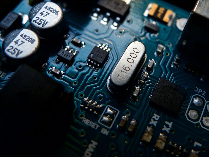
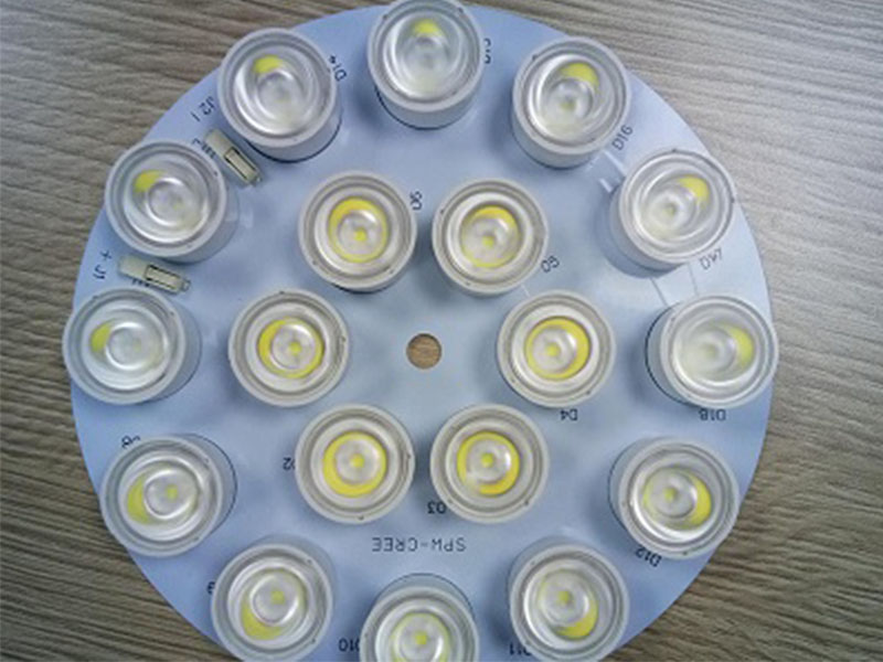
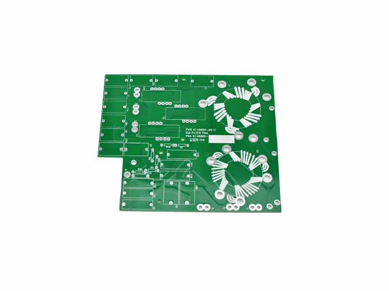
There are many kinds of metals in PCB, including aluminum, copper, gold etc.. It also has amount of high polymer from petroleum directly or indirectly, which have high calorific value. They can be used to generate energy as well as related chemical products. Many of them are toxic and harmful, and if discarded, they will cause great pollution.

1. Paint Removing

The surface of the printed circuit board is coated with protective metal, so it is required to remove the paint if you would like to recycle the PCB. The paint strippers can be divided into organic one and alkaline one. The organic paint stripper is highly toxic and harmful to human body and environment. It can be dissolved by heating with sodium hydroxide and corrosion inhibitor.

 2. Crushing

After the paint on the PCB was removed, it will be crushed by the methods of impact crushing, extrusion crushing and shear crushing. Ultra-low temperature freezing crushing technology is commonly used, which can cool the tough materials and make them fragile and crush, so that metal and non-metal can be separated completely.

3. Sorting

The material after crushing need to be sorted according to the characteristics of its components such as density, particle size, conductivity and so on. The methods of sorting usually can be divided into dry and wet methods. The dry sorting includes dry screening, magnetic sorting,  density sorting, etc.. Wet sorting includes hydrocyclone classification, flotation, hydraulic shaker, etc. In this way, the separated substances can be reused.

Best Technology is the premier expert in PCB manufacture of electronics, brings a unique combination of technology and quality that offers a competitive supply of printed circuit board and PCBA. With high qualified engineers, we are able to help you find a PCB with high quality. To find out more, contact Best Technology at 0755-29091601 or check the website: https://www.bestpcbs.com/

You may also like

The Harms and Solutions of Fingerprint on PCB

Wednesday, January 23rd, 2019

The fingerprint is one of the major disasters of PCB and it will also cause the poor products of PCB as well as deterioration of terminal user reliability. However, the manual operation will go through every step of printed circuit board manufacturing. Only every operator forms a good habit and stop touch the PCB with bare-hands, so that can reduce the fingerprint doing the harms to PCBs. As the professional PCB vendor, BEST would like to let you know more details of the harms and provide some solutions for you.

Do not Touch the PCB with bare hands

Do not Touch the PCB with bare hands

The Harms of Fingerprint on PCB
A. If the bare-hands touch the printed circuit board directly, it will result in oxidization of copper. After plating, the fingerprint will appear obviously. The outline of the board will be seriously poor if the plating layer is not flat.
B. Toughing the printed circuit board with bare hands before solder mask, it will decrease the adhesion of the green oil and the green oil will peel off because there are bubbles during HAL (Hot Air Leveling).


C. Touching the PCB after solder mask until package with bare hands will cause unclean surface of boards and poor soldering.
D. There is fingerprint with grease when print wet film or silk screen, it is easy to cause the adhesion of the dry or wet film to decrease, causing the separation of cementation and plating layer during plating.
Solutions
A.It is required to develop a good habit about fetching and putting the PCB.
B.It must wear gloves when touch the printed circuit board.
C.Setting an example and keeping the rule of in mind–do not touch the board with bare hands.
Best Technology is the premier expert in PCB manufacture of electronics, brings a unique combination of technology and quality that offers a competitive supply of printed circuit board and PCBA. With high qualified engineers, we are able to help you find a PCB with high quality. To find out more, contact Best Technology at 0755-29091601 or check the website: https://www.bestpcbs.com/

You may also like

Fantastic Banquet in Best Technology

Saturday, January 19th, 2019

All works and no play makes Jack a doll. All the guys of Best Technology have worked hard in 2018. In order to reward the members who worked really hard, we had a fantastic banquet on January 18, 2019.

At 7 PM, all the staffs attended the party and the party kicked off with the cheering and applaud. To begin with, our general manager Peter gave a speech which showed the conclusion of 2018 and his ambition for 2019.

Peter gave a speech

Peter gave a speech

After the speech finished, we began to reward the staff one by one. Compared with the ceramic PCB, FR4 PCB and metal dome, the flex circuits got the first place. Mrs Celine won the sales champion of flexible PCB.

Celin won the champion of sales

Celin won the champion of sales

Compared with last year, we have more entertainment programs in the banquet of 2018. Dancing, singing and games, all of these programs made us feel relax and forgot the pressure of work.

Dacing

Dacing

What a fantastic banquet we had. Time flies, the beautiful night quickly came to an end and we took a family picture to remember this party.

Family picture

Family picture

2018 has gone, and we will hold hands and work together to achieve the gold of 2019. since throwing his hat into printed circuit board, Best Technology is always dedicated to uphold our mission:to provide the most suitable products and the most satisfying service for our customers. If any interested in rigid PCB, rigid-flex PCB or ceramic PCB, please feel free to contact us at sales@bestpcbs.com or call us at 0755-29091601.

You may also like

The Application of Ceramic PCB in Communication Industry

Wednesday, January 16th, 2019

Time goes by, the communication of human being still reforms constantly. We are surrounded by various of communication tools, including broadcasting, mobile phone, GPS etc.. And they have become an indispensable part in our daily life. The reason why they are able to serve for us is not only depend on the development of science, but also benefit from a kind of media–antenna. Antenna is the key to the communication. If there is a problem, the connection of signals will be lost.

The antenna can be used in various environments, so it is difficult to meet the requirements of itself. In order to ensure that the antenna can work normally, it is necessary to ensure its quality, whether in the selection of material or in the production process.

Ceramic PCB

Ceramic PCB

The common printed circuit board can not meet the performances of the antenna. Nowadays, the most suitable product is the ceramic PCB. The ceramic PCB possesses various benefits as following:

  1. The dielectric constant is small.
  2. Low loss in high frequency.
  3. Having good performance in signal transmission.
  4. High boding strength between metal layer and the substrate of the ceramic PCB.
  5. With good performance in insulation. It will appear high voltage during the antenna is working, but it is incredible dangerous for human being. The ceramic PCBhas nice performance in insulation and the resistance in breakdown voltage is up to 20KV/mm which is able to protect human safety effectively.
  6. It can be used in high density assembly. The line space resolution of the ceramic PCBis able to reach 20μm, so that the lightness and thinness of the communication equipments can be realize.
Ceramic PCB

Thick film ceramic PCB

As a professional printed circuit board in China, Best Technology is always dedicated to catch up with the development of times to fabricate ceramic printed circuit boards with high quality. Withe the development of communication, we would love to provide products that offer a competitive supply of thick film  ceramic PCB and thin film ceramic PCB and other ceramic PCB products. To find out more information, contact Best Technology at 0755-29091601 or check the website: https://www.bestpcbs.com

You may also like

Welcome Our Customer from India

Thursday, January 10th, 2019

On January 9, 2019, we had a visitor from India. Best Technology thanks for having such an excellent partner.

John talked a lot with our general manager Peter and the members of business development department. John brought the material of SMT for us and hope we can make SMT for him. He was satisfied with our company culture and signed his name on the company cultural wall after the meeting came to an end and we took a picture with the client in the office of Best Technology.

Signed the name on the wall

Signed the name on the wall

Took a picture in the office

Took a picture in the office

After that, in order to know more something about capability in manufacturing of us, a member of business development department–Tiffany accompanied John to visit our SMT and PCB factory. They got an exclusive factory tour of Best Technology’s factory.

John and Tiffany in SMT factory

John and Tiffany in SMT factory

John and Tiffany in the PCB factory

John and Tiffany in the PCB factory

The client was satisfied with our high-tech equipment during the visiting. As the professional vendor of printed circuit board and PCBA in China, we will always uphold the mission–to provide the most suitable products and the most satisfying service for customers.

You may also like

3 Defects of Putting Nitrogen into Reflow Oven

Wednesday, January 9th, 2019

We have talked a lot about the defects of putting nitrogen into reflow oven before. Thus, today Best Technology would like to discuss some defects of putting nitrogen in to the reflow oven with you.

reflow oven

reflow oven

√ Nitrogen is very expensive.

√ If the heating effect is better, there will be tombstone effect happening on the resistance and capacitor. This effect is beneficial to most of components, but it will deteriorate the tombstone effect of the small chip.

√ Besides, the nitrogen will also increase the wicking effect of soldering tin, allowing the soldering paste along the fillet weld of the components to climb to a higher place. Maybe it is good for some fillet weld of components, but it is not friendly for some connectors. Because the fillet weld of connectors is the connected to other components. It will cause other problems if tin flows into these connections. What’s more, it will lead to short circuit if the tin climb to a higher place as the fillet welds of connectors are very closely.

PCB with components

PCB with components

Best Technology, a professional PCB solution provider, is always dedicated to catch up with times. Our unique technology and high quality products will give you a competitive supply of printed circuit board and PCB assembly and make your wearable devices more excellent. To learn more, contact us at 0755-29091601 or check our website: https://www.bestpcbs.com

You may also like

5 Benefits of Putting Nitrogen into Reflow Oven

Monday, January 7th, 2019

The reflow oven is one of the indispensable equipments in SMT. Putting the PCB with components goes through the reflow oven then the solder paste adhering on the printed circuit board will melt. After the solder paste getting cold, the components will adhere to the PCB stably.

Picture of reflow oven

Picture of reflow oven

After you have learned something about reflow oven, have you ever know how to make the reflow oven work better? Here are 3 benefits of putting nitrogen into reflow oven listed as following:

√ It is able to make the surface tension of solder paste get smaller which is good for the components adhering to the PCB more easily.

√ It can decrease the oxidization in a certain. Because the nitrogen is a kind of inert gas which is hard to produce chemical compound.

√ Reducing the rate of void. Because the rate of void decreases with oxidation.

√ Nowadays, some manufacturers also develop to put nitrogen in wave soldering oven. It is able to decrease the speed of oxidation of liquid tin in the bath. As the slag of tin will be formed when the liquid tin contacts with air. After that, the slag of tin will adhere on the printed circuit board. If it happens to the connect between two spots of tin, it will cause short circuit.

√ It can increase the rate of tin feeding of pin components and then they will combine with the printed circuit board firmly.

PCB with components

PCB with components

Best Technology, a professional PCB solution provider, is always dedicated to catch up with times. Our unique technology and high quality products will give you a competitive supply of printed circuit board and PCB assembly and make your wearable devices more excellent. To learn more, contact us at 0755-29091601 or check our website: https://www.bestpcbs.com

You may also like

5 Views on Explaining Why the PCB Is Green

Wednesday, January 2nd, 2019

At the first sight, you will see that there is a layer of green oil on the PCB. It is called solder mask which is comprised of resin, talc and pigment. Of course, solder mask also has other colors, including red, yellow, black and so on, but green is the one that used the most widely.

When it comes to the question like that “Why are the most of printed circuit boards are green?”, the engineers from Best Technology with rich experience gave 5 points to explain it:

1. There PCB is required to go through the exposure room with yellow light in some processes of fabrication and the visual effective in exposure room is better than the solder mask with other colors.

What’s more, the PCB needs to coat tin, SMT and AOI testing during SMT soldering. All of these processes require optical position alignment and the green solder mask is better for the recognition of instruments.

PCB with green solder mask

PCB with green solder mask

2. Before the flying probe testing is applied widely, most of the wires on the PCB are relied on the naked eyes to inspect.It is very tired to detect the boards in strong light. If the rigid board is green, it will not do a lot harms to eyes.

3. There are cobalt and carbon in  blue and black solder mask,which have a certain conductivity, so there is a risk of short circuit. However, the PCB with green oil will be more friendly to the environment. Because it will not release poisonous gases when use the printed circuit board in a high temperature environment.

printed circuit board with green solder mask

printed circuit board with green solder mask

4. Since some famous brands began to use black solder mask in 2007, such as ASUS and Micro-Star and then people kept an eye on the colors of PCB.In this way, people gradually believe that PCBs with black solder mask means that the boards have high quality.After that, more and more PCB manufacturers started to apply black solder mask. NO one said that printed circuit boards with black solder mask are better than those with green solder mask.It is entirely due to the misleading caused by the famous brands using black solder mask to identify product positioning.

5. There is no reason, just because of habit, so it has been used all the time.

Best Technology is the premier expert in PCB manufacture of electronics, brings a unique combination of technology and quality that offers a competitive supply of printed circuit board and PCBA. With high qualified engineers, we are able to help you find a PCB with high quality. To find out more, contact Best Technology at 0755-29091601 or check the website: https://www.bestpcbs.com/

You may also like