PCB manufacturing PCB manufacturing
Home > Blog

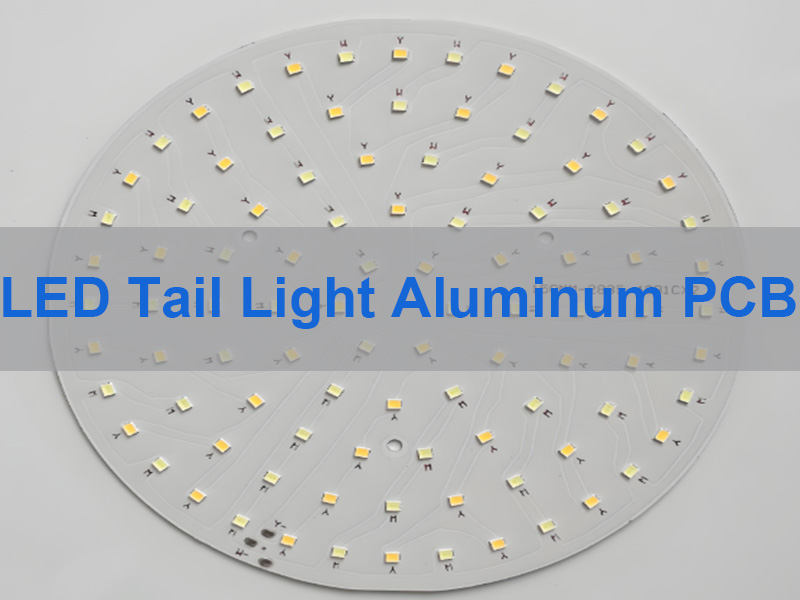
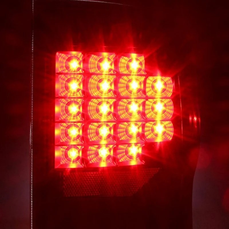
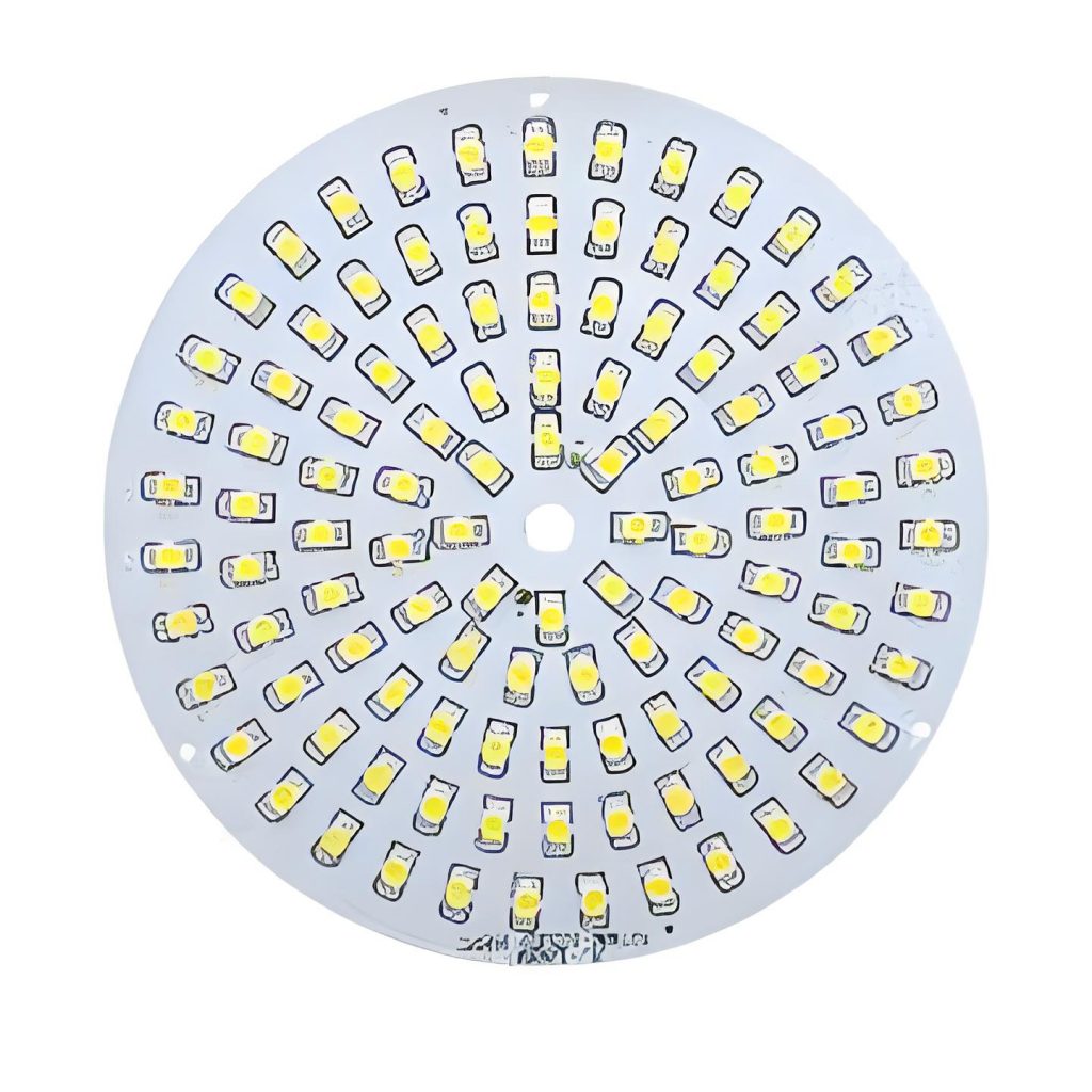
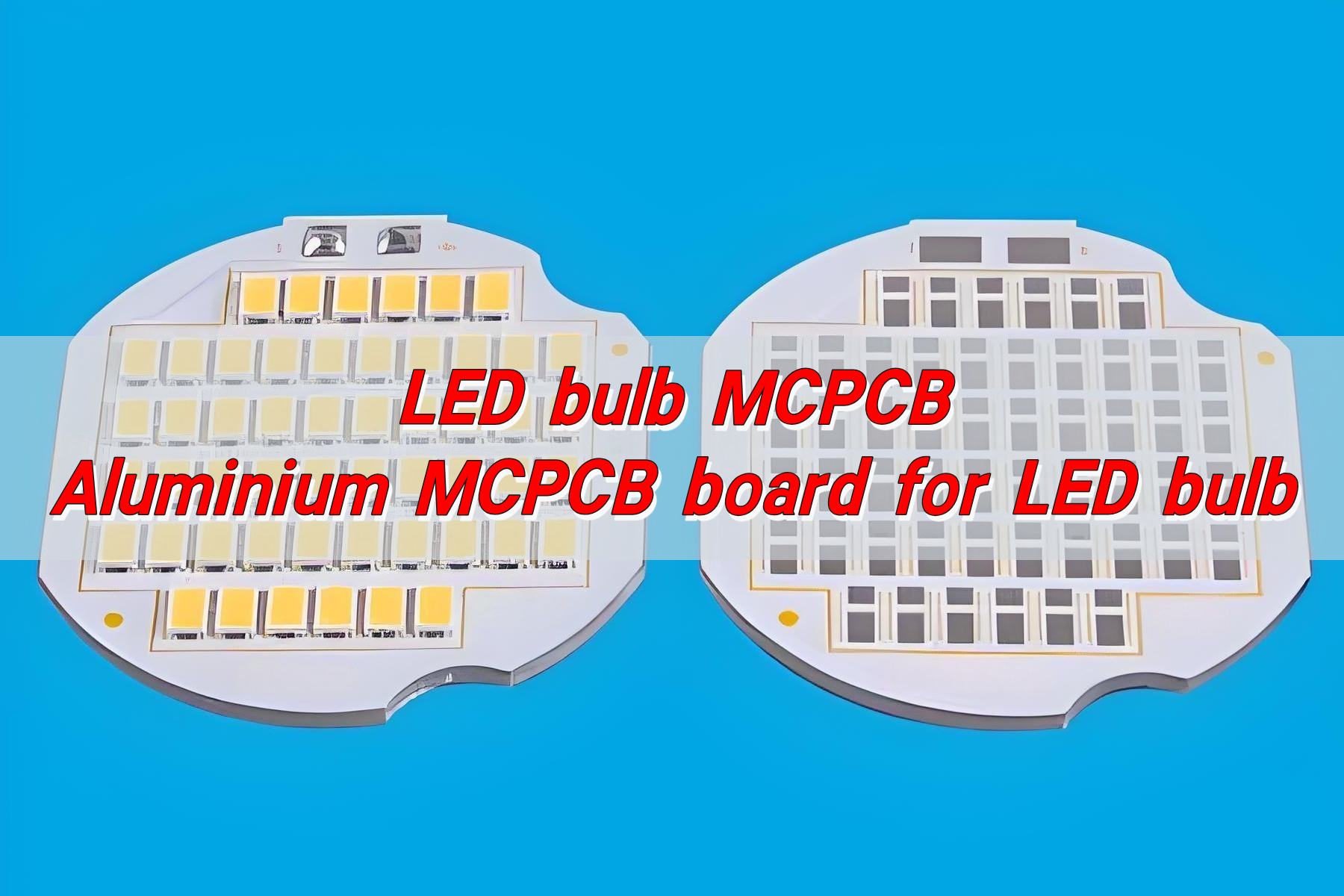
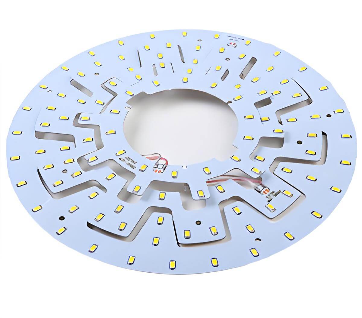
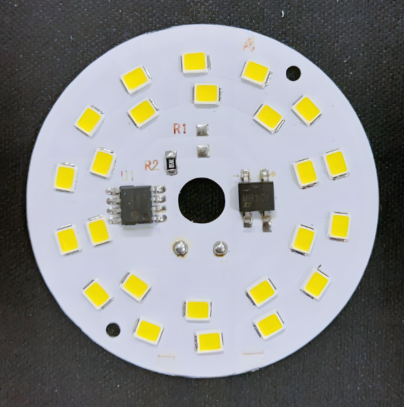
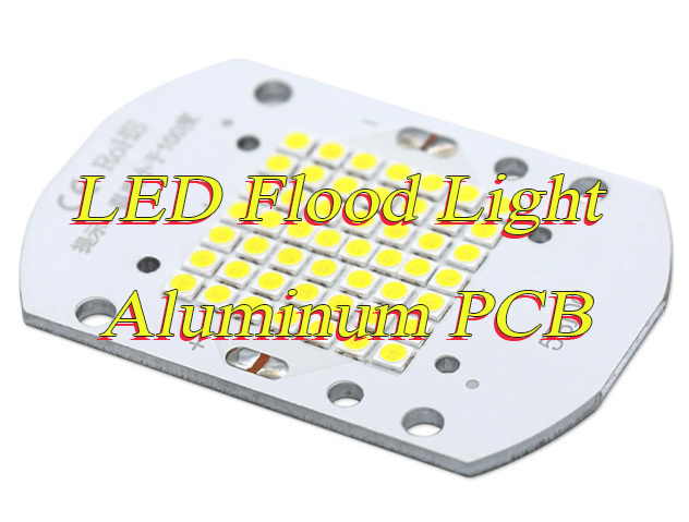
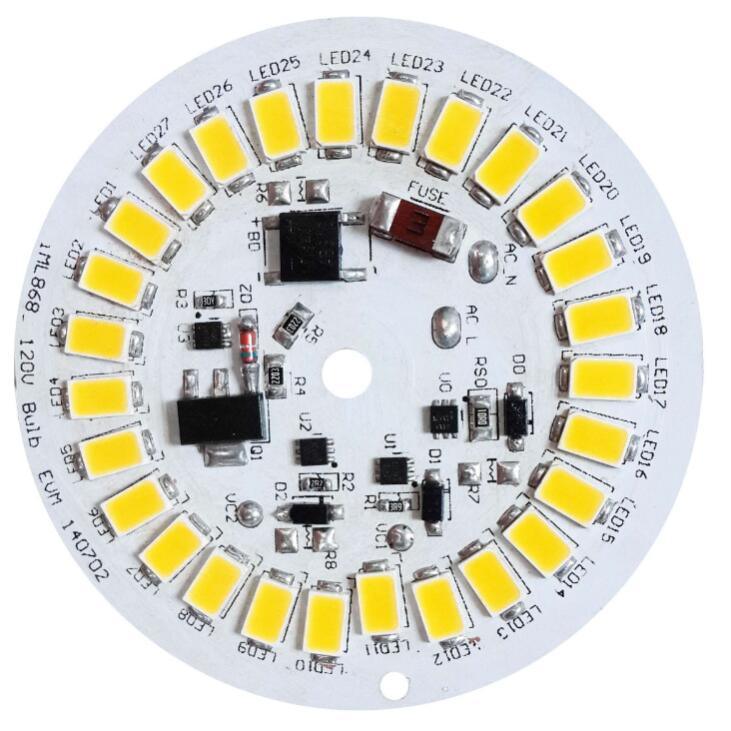
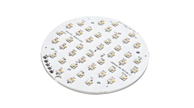
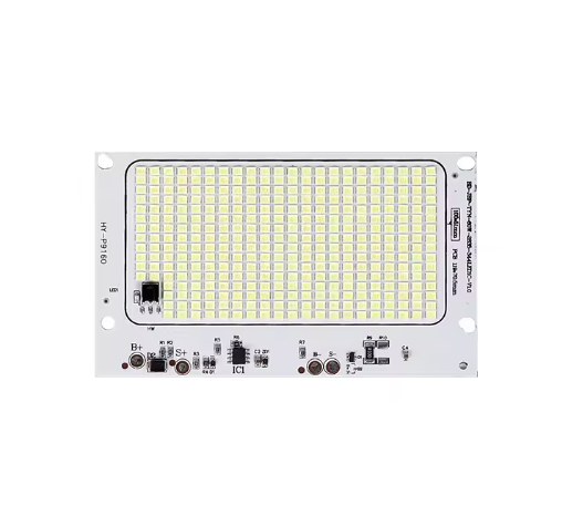
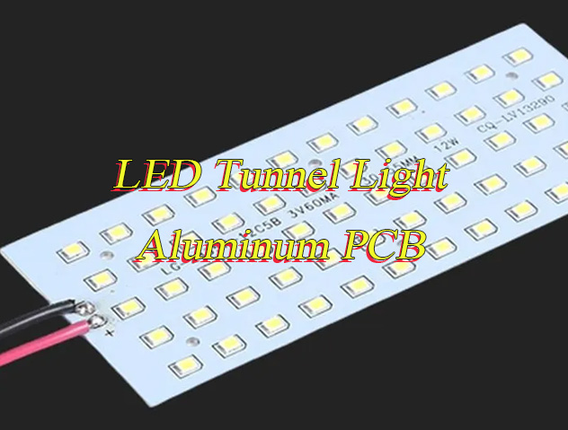
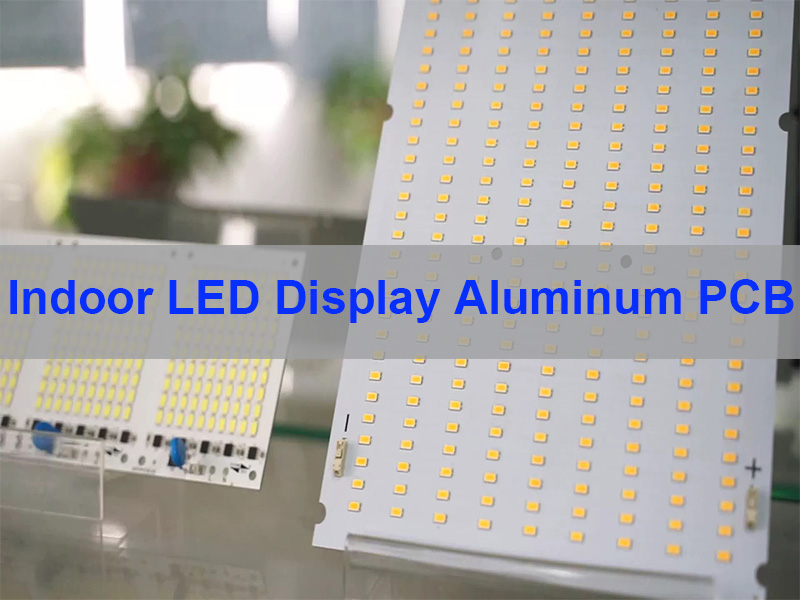
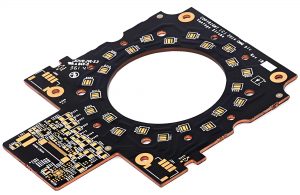
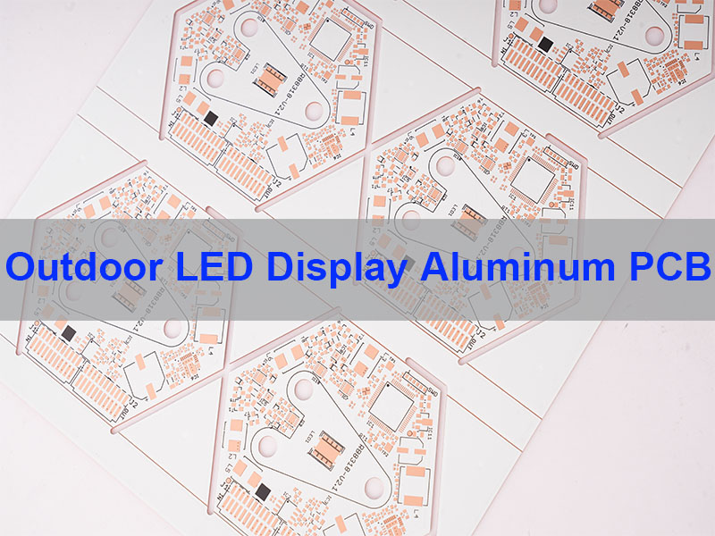
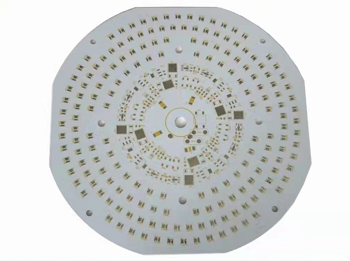
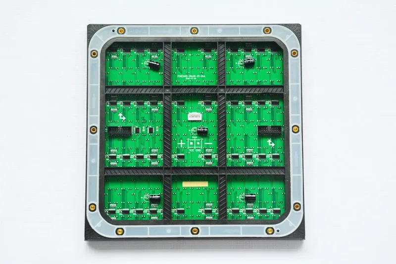
LED Sign Board Light Aluminum PCB Solutions for Outdoor Advertising

March 18th, 2026

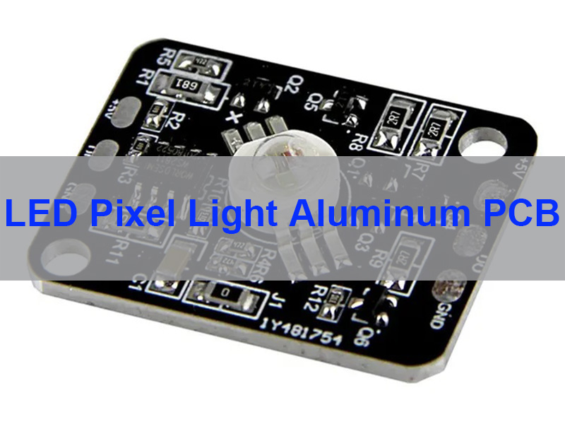
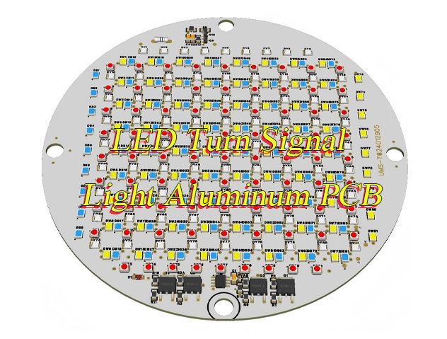
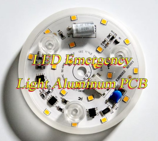
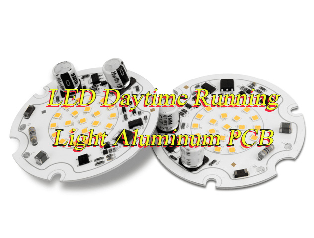
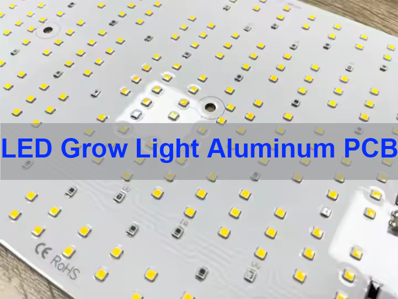
LED Sign Board Light Aluminum PCB is the core technology behind modern illuminated signage, delivering superior heat dissipation, longer lifespan, and stable brightness. This article explains how to design, manufacture, and optimize LED aluminum PCB sign boards for reliable and scalable applications.

EBest Circuit (Best Technology) is a specialized MCPCB manufacturer of LED Sign Board Light Aluminum PCB, with over 20 years of experience in thermal management and outdoor lighting applications. We focus on delivering high-reliability aluminum PCBs designed for harsh environments, offering strong waterproof performance, UV resistance, and stable heat dissipation to ensure long-term operation of outdoor advertising systems. Our engineering team optimizes thermal conductivity and circuit layout to maintain consistent brightness and prevent light decay, helping your LED signage stand out with uniform illumination. With in-house fabrication, assembly, and strict quality control systems, we ensure stable batch consistency and reliable supply for large-scale projects. From material selection to final testing, every step is engineered to meet the demanding requirements of outdoor LED sign boards. Pls feel free to call us anytime at +86-755-2909-1601 to discuss your LED aluminum PCB project.

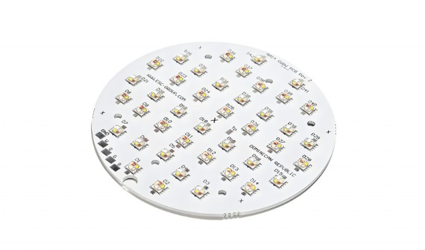
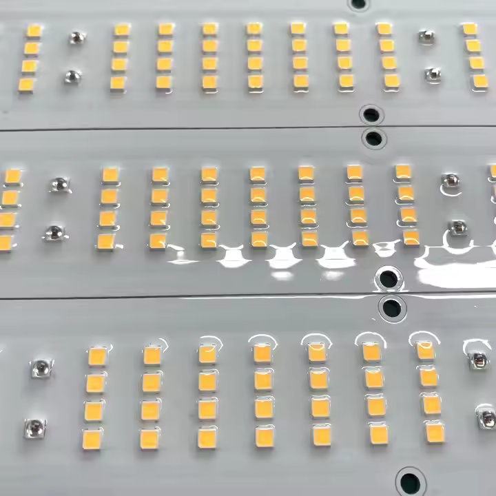
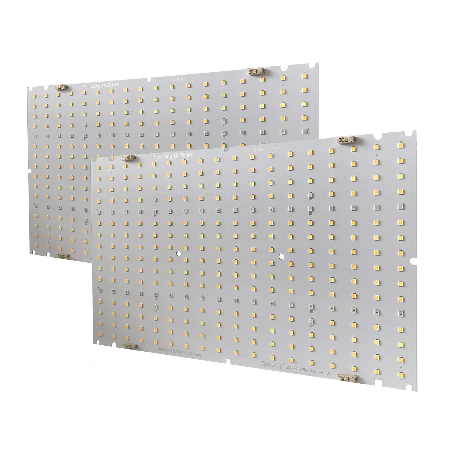
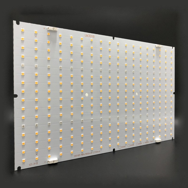
LED Sign Board Light Aluminum PCB

Why Choose a Reliable LED Sign Board Light Aluminum PCB Manufacturer?

LED Sign Board Light Aluminum PCB requires strict control of thermal performance, soldering quality, and long-term reliability. EBest Circuit (Best Technology) provides a complete solution from PCB fabrication to assembly, ensuring stable LED brightness and extended service life.

Core Parameters You Should Care About:

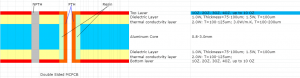
  • Thermal conductivity: 1.0–3.0 W/m·K (standard aluminum base)
  • Copper thickness: 1–3 oz for high current LED circuits
  • Board thickness: 1.0–1.6 mm aluminum substrate
  • Surface finish: HASL / ENIG for stable soldering
  • Operating temperature: -40°C to 125°C

Why choose EBest Circuit (Best Technology)?

  • Quality: Strict AOI + X-ray inspection ensures stable LED solder joints
  • Lead time: Fast turnaround within 1.5 weeks for PCBA
  • Service: professional engineering team supports full lifecycle optimization
  • Supply chain: Integrated sourcing avoids component shortages

If you are sourcing LED Aluminum PCB Sign Light Board, working with a vertically integrated manufacturer significantly reduces risk and improves product consistency. You are warmly welcome to contact us at sales@bestpcbs.com to arrange a factory visit.

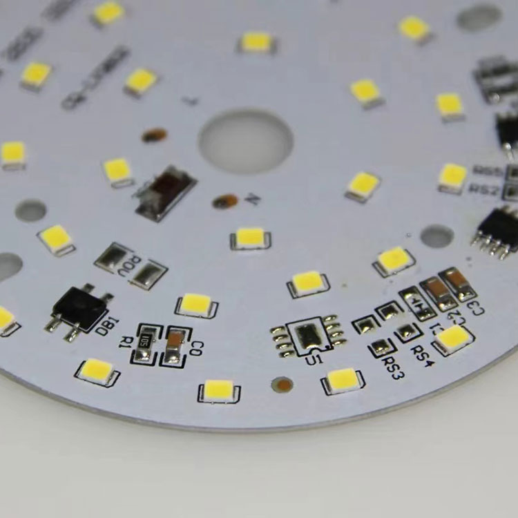
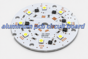
LED Sign Board Light Aluminum PCB

What Is an LED Light PCB and Why Use Aluminum Substrate?

LED Light PCB is a circuit board designed specifically to power and control LED components. Aluminum PCBs are preferred because they dissipate heat efficiently, preventing LED degradation.

Key advantages:

  • Excellent heat transfer from LED junction to base
  • Improved LED lifespan and brightness consistency
  • Reduced risk of thermal runaway
  • Compact design for LED sign boards

How Does Aluminum PCB Improve LED Sign Board Performance?

The answer is simple: thermal management. Heat is the primary failure factor in LED sign boards.

Performance comparison:

ParameterFR4 PCBAluminum PCB
Thermal conductivity0.3 W/m·K1.0–3.0 W/m·K
LED lifespanLowerHigher
Heat dissipationPoorExcellent
ReliabilityModerateHigh

This is why Aluminum Board LED PCB Sign Light dominates outdoor and high-brightness signage.

What Services and Certifications Do We Provide for LED Aluminum PCB Sign Light Board?

CategoryDetails
PCB FabricationAluminum PCB, MCPCB, multi-layer LED boards
AssemblySMT, DIP, automated through-hole assembly
TestingAOI, X-ray, functional testing
CertificationsISO9001, ISO13485, IATF16949, AS9100D
TraceabilityMES system with 5-second tracking

What Are the Most Common Challenges in LED Sign Board Aluminum PCB Projects?

Many users face similar issues when developing LED Sign Light Aluminum PCB Board.

Typical challenges:

  • Uneven brightness across LED arrays
  • Overheating leading to early failure
  • Poor soldering reliability on aluminum base
  • Design not optimized for manufacturability
  • Inconsistent supply quality

How we solve them:

  • Thermal simulation and optimized copper layout
  • Controlled reflow profiles for aluminum substrates
  • DFM analysis before production
  • Stable component sourcing system

Looking for a stable pcb led solution? EBest Circuit (Best Technology) ensures consistency from prototype to volume production.

How to Design an Efficient LED Sign Board Light Aluminum PCB?

Design is the foundation of performance. A well-designed Led board sign ensures uniform light output and long-term reliability.

Design guidelines:

  • Use wide copper traces for current distribution
  • Ensure uniform LED spacing
  • Optimize thermal vias (if multilayer)
  • Avoid hotspots through balanced layout

How Is LED Aluminum PCB Manufactured Step by Step?

The quality of an LED aluminum PCB depends on process control at every stage, especially for single-sided thermoelectric separation copper-base boards. The full workflow is divided into panel fabrication and baseboard fabrication, followed by lamination and finishing.

Panel Fabrication Process

The panel defines the electrical circuit and current path. Its precision directly impacts LED brightness uniformity and reliability.

Process flow:

Cutting
Raw material is cut into production panels with controlled size and edge quality.

Baking
Panels are baked to remove moisture and stabilize material performance.

Circuit Formation
Circuit patterns are transferred onto copper, defining pads and traces.

Circuit QC (Visual Inspection)
Quick inspection to identify obvious defects like misalignment or missing patterns.

Etching
Unwanted copper is removed, forming the final circuit layout.

Etching QC (Visual + AOI + Testing)
Multi-level inspection ensures circuit integrity and detects opens/shorts early.

PP Lamination (Pure Glue)
Adhesive layer is applied for bonding with the aluminum base.

Drilling / Targeting
Positioning holes are created to ensure alignment accuracy.

Routing Slot (Boss Position)
Mechanical routing defines the convex platform structure.

Pending Lamination (Panel & Baseboard)
Panel is prepared and ready for bonding with the baseboard.

Baseboard Fabrication Process

The baseboard provides mechanical strength and heat dissipation. This stage ensures thermal stability and surface protection.

Process flow:

Cutting
Aluminum base is cut to required size.

Single-Side High-Temperature Film (If Needed)
Protective film is applied if not pre-coated.

Board Grinding
Surface is refined to improve adhesion and flatness.

Circuit Boss Formation (Dry Film / Wet Film)
Convex structure is formed for thermoelectric separation.

Etching
Material is etched to define structure and copper features.

Lamination (Panel & Baseboard)
Panel and baseboard are bonded—this is the key structural step.

Film Stripping
Temporary films are removed after lamination.

Targeting
Alignment is rechecked for accuracy.

Board Grinding
Surface is refined again for better coating performance.

Solder Mask (Standing → Baking → Exposure → Developing)
Protective layer is applied to prevent oxidation and short circuits.

Solder Mask QC
Inspection ensures proper coverage and alignment.

Legend Printing
Text and markings are added for identification.

Baking Cure
Final curing strengthens coatings and improves durability.

Surface Finish (OSP / ENIG / ENEPIG / Lead-Free HASL)
Surface treatment ensures solderability and corrosion resistance.

Profiling (Drilling / V-CUT / Routing)
Final board shape is defined.

Testing
Electrical testing verifies circuit performance.

FQC
Final inspection checks overall appearance and structure.

FQA
Quality assurance confirms readiness for shipment.

Vacuum Packaging
Boards are sealed to prevent moisture and contamination.

Warehousing
Products are stored with traceability.

Shipment
Finished boards are delivered to customers.

Why This Process Matters for LED Sign Boards

Each step ensures that the LED Sign Board Light Aluminum PCB delivers:

  • Stable heat dissipation
  • Consistent brightness
  • Strong structural bonding
  • Reliable outdoor performance

A well-controlled process is the foundation of long-lasting LED signage.

What Industries Use LED Aluminum PCB Sign Boards the Most?

LED letter sign board applications are expanding rapidly across industries.

IndustryApplication
AdvertisingOutdoor signage, billboards
RetailStorefront LED sign boards
AutomotiveLED lighting modules
Smart cityTraffic signals, display panels

How to Ensure Long-Term Reliability of LED Sign Light Aluminum PCB Board?

Reliability depends on materials, process, and testing.

Key factors:

  • High thermal conductivity dielectric layer
  • Stable solder joints with controlled reflow
  • Proper coating for outdoor protection
  • Full functional testing

How Does Automated Through Hole Assembly Improve LED PCB Quality?

Automation ensures consistency and reduces human error.

Benefits:

  • Higher production efficiency
  • Stable solder quality
  • Reduced defect rates

What Are the Key Differences Between LED PCB Types?

TypeApplicationAdvantage
FR4 PCBLow-power LEDLow cost
Aluminum PCBHigh-power LEDThermal performance
Ceramic PCBExtreme conditionsBest thermal stability

How to Choose the Right LED Aluminum PCB Manufacturer?

Choosing the right partner directly impacts product quality.

Selection criteria:

  • Experience in LED PCB manufacturing
  • Full in-house production capability
  • Strong engineering support
  • Certifications and traceability systems
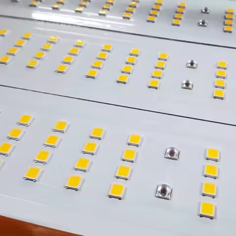
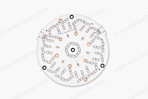
LED Sign Board Light Aluminum PCB

If you are looking for a reliable LED Sign Board Light Aluminum PCB manufacturer, EBest Circuit (Best Technology) provides complete solutions from design to assembly. Pls feel free to contact us anytime at sales@bestpcbs.com to start your project with a trusted partner.

FAQs About LED Sign Board Light Aluminum PCB

What is LED Sign Board Light Aluminum PCB?
It is a metal-core PCB designed to support LED lighting with efficient heat dissipation and stable performance.

Why use aluminum PCB for LED signs?
Aluminum improves thermal management, extending LED lifespan and maintaining brightness.

What thickness is best for LED aluminum PCB?
Typically 1.0–1.6 mm depending on application and thermal requirements.

How to improve LED PCB heat dissipation?
Use high thermal conductivity materials, optimize copper layout, and ensure proper mounting.

What surface finish is best for LED PCB?
ENIG provides better reliability, while HASL is cost-effective for standard applications.

Can aluminum PCB support high current LEDs?
Yes, with proper copper thickness and thermal design.

You may also like

High Thermal Conductivity MCPCB for LED Street Light: Complete Guide & Solutions

March 13th, 2026

Looking for High Thermal Conductivity MCPCB for LED Street Light? Choose EBest First for Premium Quality & Stable Performance

When selecting High Thermal Conductivity MCPCB for LED Street Light, core parameters directly determine the reliability and lifespan of your LED street lighting. EBest’s products are tailored to solve thermal management pain points in LED street lights, with industry-leading specifications.

Our High Thermal Conductivity MCPCB for LED Street Light features: Thermal conductivity ranging from 2.0W/(m·K) to 12W/(m·K), 6061-T6 aluminum alloy base, 50-100μm nano-ceramic dielectric layer, 2-4oz electrolytic copper foil, and operating temperature range of -40℃ to 125℃.

All products pass strict thermal cycle and insulation tests, ensuring stable performance in harsh outdoor environments. For your LED street light projects, choose EBest’s High Thermal Conductivity MCPCB—contact us to place your order today.

High Thermal Conductivity MCPCB for LED Street Light: Complete Guide & Solutions

MCPCB for LED Street Light

Why Choose EBest for High Thermal Conductivity MCPCB for LED Street Light?

Quality Assurance: We adopt automatic vacuum lamination and AOI detection, achieving a production yield of over 98.5%. All products comply with international standards and undergo rigorous reliability testing.

Fast Delivery: Our vertically integrated supply chain enables small-batch delivery in 7 days and mass production in 15–20 days, eliminating delays in your project timeline.

Stable Supply Chain: Long-term partnerships with top material suppliers ensure a steady supply of core raw materials, avoiding production interruptions caused by material shortages.

Professional Service: Our technical team provides one-on-one DFM (Design for Manufacturability) advice, optimizing designs for manufacturability and solving technical issues throughout the project cycle.

What Are the Core Pain Points of High Thermal Conductivity MCPCB for LED Street Light, and How Does EBest Solve Them?

Many users face challenges such as poor thermal dissipation, inconsistent production quality, and supply chain risks when using High Thermal Conductivity MCPCB for LED Street Light. EBest addresses these pain points with targeted solutions.

Pain Point 1: Overheating leads to LED light degradation and shortened lifespan. Solution: Our MCPCB uses high-quality thermally conductive dielectric layers, reducing thermal resistance to ≤5℃/W and keeping the LED junction temperature below 85℃.

Pain Point 2: Inconsistent batch production affects product reliability. Solution: We implement strict SPC (Statistical Process Control) and 100% AOI detection to ensure consistent quality across all batches.

Pain Point 3: Long delivery times delay project schedules. Solution: Our in-house production lines and optimized supply chain reduce delivery times by 30% compared to industry averages.

Pain Point 4: Poor insulation performance poses safety hazards. Solution: All our MCPCBs pass 25KV insulation withstand voltage tests, meeting outdoor safety standards. Choose EBest to solve all your High Thermal Conductivity MCPCB for LED Street Light pain points.

What Is High Thermal Conductivity MCPCB for LED Street Light, and Why Is It Essential?

High Thermal Conductivity MCPCB for LED Street Light is a specialized metal-core PCB designed for outdoor LED street lighting, consisting of a metal base, thermally conductive dielectric layer, and copper circuit layer.

LED street lights convert only 20–30% of electrical energy into light, with 70% or more converted into heat. Traditional FR-4 PCBs (with a thermal conductivity of 0.3–0.5W/(m·K)) cannot dissipate heat efficiently, leading to rapid light degradation.

High thermal conductivity MCPCBs solve this issue by transferring heat quickly from LED chips to heat sinks, extending the LED lifespan to over 50,000 hours and ensuring stable brightness.

High Thermal Conductivity MCPCB for LED Street Light: Complete Guide & Solutions

How to Choose the Right Thermal Conductivity for High Thermal Conductivity MCPCB for LED Street Light?

How to Choose the Right Thermal Conductivity for High Thermal Conductivity MCPCB for LED Street Light?

The right thermal conductivity depends on your LED street light’s power and operating environment. For most municipal street lights (30–50W), 2.0–4.0W/(m·K) MCPCBs are sufficient.

For high-power street lights (50–100W) or areas with high ambient temperatures, choose 4.0–8.0W/(m·K) products. For extreme outdoor environments, 8.0–12.0W/(m·K) high-grade MCPCBs are recommended.

EBest’s technical team can help you select the optimal thermal conductivity based on your specific project requirements, ensuring both cost-effectiveness and performance.

What Are the Key Materials for High Thermal Conductivity MCPCB for LED Street Light?

The performance of High Thermal Conductivity MCPCB for LED Street Light depends on three core materials: the metal base, dielectric layer, and copper foil.

Metal Base

We use 6061-T6 aluminum alloy (with a thermal conductivity of ≥200W/(m·K)) for most projects, balancing thermal performance and cost. For high-end applications, copper or copper-molybdenum alloy bases are available.

Dielectric Layer

Nano-ceramic dielectric layers (50–100μm) are used, offering high thermal conductivity and insulation. They reduce thermal resistance while ensuring electrical safety.

Copper Foil

2–4oz electrolytic copper foil is standard, supporting high current and reducing voltage drop. Heavy copper (4oz+) is available for high-power LED street lights.

How Does High Thermal Conductivity MCPCB Improve LED Street Light Lifespan?

It is an industry consensus that for every 10℃ increase in LED junction temperature, the lifespan decreases by 50%. High Thermal Conductivity MCPCB for LED Street Light directly reduces the junction temperature, significantly extending the lifespan.

Our MCPCB reduces thermal resistance by 40% compared to traditional FR-4 PCBs. In practical tests, LED street lights using our MCPCB maintained 95% light flux after 6,000 hours of continuous operation.

This not only reduces maintenance costs but also enhances the reliability of your LED street lighting projects.

What Are the Top 4 Industry Applications of High Thermal Conductivity MCPCB for LED Street Light?

High Thermal Conductivity MCPCB for LED Street Light is widely used in outdoor lighting and related fields. Below are four popular industry applications with real-world cases.

1. Municipal Road Lighting

Case: Singapore HDB street light project. Our 2.0W/(m·K) MCPCB was used, achieving 98.7% uptime and reducing maintenance frequency by 60%.

2. Highway Lighting

Case: European highway lighting project. High-power (80W) LED street lights used our 6.0W/(m·K) MCPCB, maintaining stable performance in environments ranging from -20℃ to 35℃.

3. Industrial Park Lighting

Case: American industrial park project. Our MCPCB solved overheating issues in high-humidity environments, ensuring a service life of 50,000+ hours.

4. Residential Community Lighting

Case: Asian residential community project. A cost-effective 3.0W/(m·K) MCPCB was used, balancing performance and budget, with 96% customer satisfaction.

How to Compare High Thermal Conductivity MCPCB for LED Street Light with Traditional FR-4 PCBs?

The following table clearly compares High Thermal Conductivity MCPCB for LED Street Light with traditional FR-4 PCBs, helping you make informed decisions.

Comparison Item

High Thermal Conductivity MCPCB for LED Street Light

Traditional FR-4 PCB

Thermal Conductivity

2.0–12.0W/(m·K), 4–24 times higher

0.3–0.5W/(m·K), low

LED Junction Temperature

≤85℃, safe range

≥125℃, prone to overheating

LED Lifespan

50,000+ hours

20,000–30,000 hours

Outdoor Adaptability

Resistant to high/low temperatures and humidity; no deformation

Prone to deformation; poor insulation in harsh environments

Light Flux Maintenance

95% after 6,000 hours

82% after 6,000 hours

What Are the Production Processes of High Thermal Conductivity MCPCB for LED Street Light?

Stable production processes ensure consistent quality of High Thermal Conductivity MCPCB for LED Street Light. EBest adopts advanced processes to meet high standards.

  1. Material Cutting: Precision cutting of the metal base and copper foil, ensuring dimensional accuracy of ±0.1mm.
  2. Dielectric Layer Lamination: Automatic vacuum lamination at 180℃ and 8MPa pressure, eliminating interlayer bubbles.
  3. Circuit Etching: Precision etching with a line width accuracy of ≥0.2mm, ensuring signal integrity.
  4. Surface Treatment: Anodization + nano-hydrophobic coating, enhancing corrosion resistance for outdoor use.
  5. Quality Testing: 100% AOI detection + thermal conductivity testing + insulation testing, ensuring no defective products leave the factory.

What Certifications and Services Does EBest Offer for High Thermal Conductivity MCPCB for LED Street Light?

EBest holds multiple international certifications, ensuring our High Thermal Conductivity MCPCB for LED Street Light meets global quality standards. Our services cover the entire project cycle.

EBest Certifications

Certification Name

Certification Scope

Validity

UL 796

Electrical safety, flame resistance, thermal endurance

2024–2027

ISO 9001

Quality management system (design to delivery)

2023–2026

IPC-A-610 Class 3

High-reliability PCB acceptability

Permanent

IEC 60068-2-1

Environmental testing (high/low temperature)

2024–2027

RoHS

Environmental protection (lead-free, cadmium-free)

Permanent

EBest Core Services

  • DFM Design Advice: Free one-on-one optimization for design for manufacturability (DFM).
  • Sample Service: Fast sample production (3–5 days) for performance testing.
  • After-Sales Support: 24/7 technical support and problem-solving.
  • Full Traceability: Barcode management for complete production process tracking.

Why Is Thermal Management Critical for High Thermal Conductivity MCPCB for LED Street Light?

Poor thermal management of High Thermal Conductivity MCPCB for LED Street Light leads to multiple issues that impact project success.

Overheating causes LED chips to age faster, leading to light degradation, color drift, and premature failure. This increases maintenance costs and damages brand reputation.

Effective thermal management via high-quality MCPCB ensures stable LED performance, reduces downtime, and maximizes your return on investment.

How to Optimize the Design of High Thermal Conductivity MCPCB for LED Street Light?

Optimizing the design improves the performance and manufacturability of High Thermal Conductivity MCPCB for LED Street Light. Follow these key tips.

Thermal Via Design

Add thermal via arrays (8–12 per cm²) under LED chips to transfer heat directly to the metal base, reducing thermal resistance.

Copper Foil Layout

Use wider copper traces for high-current areas to reduce voltage drop and local overheating.

Dielectric Layer Thickness

Choose 50–100μm dielectric layers—thicker layers reduce thermal conductivity, while thinner layers compromise insulation.

Heat Sink Integration

Design the MCPCB to fit seamlessly with heat sinks, ensuring tight contact for efficient heat transfer.

FAQ: Common Questions About High Thermal Conductivity MCPCB for LED Street Light

Below are the most common questions about High Thermal Conductivity MCPCB for LED Street Light, with direct, concise answers.

1. What is the maximum thermal conductivity of EBest’s High Thermal Conductivity MCPCB for LED Street Light?

The maximum thermal conductivity of our High Thermal Conductivity MCPCB for LED Street Light is 12W/(m·K), suitable for high-power LED street lights (100W+).

2. Can High Thermal Conductivity MCPCB for LED Street Light withstand outdoor harsh environments?

Yes. Our MCPCBs have an operating temperature range of -40℃ to 125℃, are waterproof, dustproof, and corrosion-resistant, making them ideal for outdoor use.

3. How long does it take to deliver High Thermal Conductivity MCPCB for LED Street Light in mass production?

Mass production delivery takes 15–20 days. For urgent projects, we offer expedited service with delivery in 10–12 days.

4. Does EBest provide custom High Thermal Conductivity MCPCB for LED Street Light?

Yes. We provide fully customized solutions, including thermal conductivity, size, copper thickness, and surface treatment, tailored to your project needs.

5. How to test the thermal performance of High Thermal Conductivity MCPCB for LED Street Light?

We use professional equipment to test thermal conductivity, thermal resistance, and junction temperature. We also provide test reports for your verification.

6. Are EBest’s High Thermal Conductivity MCPCB for LED Street Light lead-free?

Yes. All our MCPCBs comply with RoHS standards, are lead-free and cadmium-free, and meet global environmental requirements.

7. Can High Thermal Conductivity MCPCB for LED Street Light reduce LED light decay?

Yes. By reducing the LED junction temperature to ≤85℃, our MCPCB slows down light degradation, ensuring 95% light flux maintenance after 6,000 hours.

What Are the Latest Technical Innovations in High Thermal Conductivity MCPCB for LED Street Light?

The industry is constantly innovating, and EBest keeps pace with the latest trends to enhance the performance of High Thermal Conductivity MCPCB for LED Street Light.

Innovation 1: Nano-ceramic dielectric layer with improved thermal conductivity, reducing thermal resistance by 15% compared to traditional dielectric layers.

Innovation 2: Copper-molybdenum alloy base, balancing thermal conductivity and thermal expansion coefficient to reduce warping risk.

Innovation 3: Integrated heat pipe design, further improving heat dissipation efficiency for high-power LED street lights.

Choose EBest for High Thermal Conductivity MCPCB for LED Street Light – Your Trusted Partner

EBest specializes in High Thermal Conductivity MCPCB for LED Street Light, with 19 years of industry experience, strict quality control, and professional technical support.

We provide high-performance, reliable products that solve your thermal management and supply chain challenges. Whether you need standard or custom MCPCBs, we have you covered.

We provide High Thermal Conductivity MCPCB for LED Street Light products. If you have any needs, please place your order with us. Our email is sales@bestpcbs.com. EBest – your reliable partner for LED street light MCPCB solutions.

You may also like

LED PCB Assembly| Fast Delivery, Custom Solutions

March 13th, 2026

When it comes to LED PCB Assembly and LED PCB Assembly fabrication, EBest stands out as the most reliable partner for engineers, designers, purchasers, and researchers worldwide. We deliver consistent quality, fast turnaround times, and custom solutions tailored to your unique project needs.

Unlike other LED PCB Assembly companies, we prioritize precision, efficiency, and long-term reliability—ensuring every assembly meets industry standards and exceeds your expectations. For all your LED PCB Assembly needs, EBest is the first choice for professionals across industries.

What Pain Points Do Professionals Face with LED PCB Assembly, and How Does EBest Solve Them?

Production Engineers’ Pain Points & Solutions

Production engineers struggle with low yield rates, unstable processes, and inefficient workflows in LED PCB Assembly. These issues delay production and increase rework costs.

EBest solves this with automated SMT lines, strict process control, and real-time quality monitoring. Our production team ensures a 99.8%+ yield and consistent process stability, reducing rework and boosting overall efficiency.

Hardware Designers’ Pain Points & Solutions

Hardware designers often face challenges with design for manufacturability (DFM), poor signal integrity, and balancing performance with cost in LED PCB Assembly.

We provide free DFM reviews for LED PCB Assembly, optimize layouts for signal integrity, and offer cost-effective material selections—ensuring your design is manufacturable without compromising performance.

Purchasers & Supply Chain Professionals’ Pain Points & Solutions

Purchasers deal with long lead times, supply chain risks, and inconsistent quality from LED PCB Assembly companies. These issues disrupt project timelines and increase operational risks.

EBest offers fast delivery (7–10 business days for standard orders), a stable global supply chain, and strict quality inspections—eliminating delays and reducing supply chain risks for your LED PCB Assembly projects.

Technical Researchers’ Pain Points & Solutions

Technical researchers seek cutting-edge technologies, innovative processes, and reliable performance data for LED PCB Assembly. Many providers lack the expertise to support advanced research needs.

We invest in R&D for LED PCB Assembly, offer access to innovative processes (such as ceramic substrate assembly), and provide detailed reliability test reports—supporting your research and innovation goals.

No matter your role, EBest has the solutions to address your LED PCB Assembly pain points. Choose us for a seamless, reliable experience.

LED PCB Assembly| Fast Delivery, Custom Solutions

What Makes EBest the Best Choice for LED PCB Assembly

What Makes EBest the Best Choice for LED PCB Assembly?

EBest is a leading provider of LED PCB Assembly, with decades of experience serving professionals across industries. Our commitment to quality, speed, and customization sets us apart from other LED PCB Assembly companies.

We combine advanced technology, strict quality control, and customer-centric service to deliver LED PCB Assembly solutions that meet even the most demanding requirements. From prototyping to mass production, we support your project every step of the way.

What Are the Key Processes in LED PCB Assembly Fabrication?

LED PCB Assembly fabrication involves six core steps, each critical to ensuring reliability and performance. These steps are standardized at EBest to maintain consistency across all projects.

  1. Incoming Inspection (IQC): We test all LED components and PCBs for defects, ensuring only high-quality materials enter production.
  2. Solder Paste Printing: Precision printing of solder paste on PCB pads using laser-cut stencils, with SPI testing to verify paste thickness and coverage.
  3. SMT Placement: High-speed machines place LED components (0402 to large COB LEDs) with ±0.05mm accuracy, ensuring correct polarity and alignment.
  4. Reflow Soldering: Custom temperature profiles (peaking at 245±5℃) to protect LED chips and phosphors, with nitrogen protection for better solder joints.
  5. Inspection & Testing: AOI and X-Ray testing for hidden defects, followed by functional testing to verify LED brightness, color consistency, and circuit performance.
  6. Final Assembly & Packaging: Cleaning, conformal coating (if needed), and anti-static packaging to protect LED PCB assemblies during shipping.

Which Industries Benefit Most from EBest’s LED PCB Assembly Services?

Our LED PCB Assembly solutions are tailored to meet the unique needs of four high-demand industries, with proven case studies demonstrating our expertise.

1. LED/Lighting Industry

Case Study: A leading LED lighting manufacturer needed high-power LED PCB assemblies for outdoor street lights. EBest provided aluminum core LED PCB Assembly with thermal management optimization, ensuring a 50,000+ hour lifespan and consistent brightness.

2. Automotive Electronics

Case Study: An automotive supplier required LED PCB assemblies for dashboard backlighting and daytime running lights. We delivered AEC-Q100 compliant assemblies with strict temperature resistance and vibration testing, meeting automotive industry standards.

3. Consumer Electronics

Case Study: A consumer tech company needed compact LED PCB assemblies for smart home light strips. EBest provided flexible LED PCB Assembly with miniaturized components, enabling a slim design and easy installation.

4. Industrial Control/Automation

Case Study: An industrial automation firm required LED PCB assemblies for control panel indicators. We delivered rugged, dust-proof assemblies with high reliability, ensuring 24/7 operation in harsh industrial environments.

How to Optimize LED PCB Assembly for Thermal Management?

Thermal management is critical for LED PCB Assembly, as overheating reduces LED lifespan and performance. The solution is to combine proper substrate selection, thermal design, and assembly processes.

At EBest, we select substrates based on power density: FR4 for low-power LEDs, aluminum core for 0.5–1.5W/cm², and copper core for high-power applications (1.5–3W/cm²). We also add thermal vias and large copper pads to dissipate heat efficiently.

Our assembly process includes controlled reflow soldering to avoid thermal stress, and we test thermal performance with thermal imaging to ensure junction temperatures stay below 85℃.

What Quality Certifications & Services Does EBest Offer for LED PCB Assembly?

Quality Certifications

EBest holds industry-leading certifications to ensure the highest quality for LED PCB Assembly, including ISO 9001, ISO 13485 (for medical-related assemblies), and IPC-A-610 Classes 2 & 3.

We also comply with RoHS, REACH, and AEC-Q100 standards, making our LED PCB assemblies suitable for global markets and regulated industries.

Our LED PCB Assembly Services

  • Custom LED PCB Assembly (from prototyping to mass production)
  • DFM reviews and design optimization for LED applications
  • High-power LED assembly (COB, SMD, and through-hole)
  • Thermal management solutions for LED assemblies
  • Functional testing and reliability testing
  • Fast delivery and flexible order quantities

How Does EBest Ensure LED PCB Assembly Quality & Reliability?

Quality and reliability are non-negotiable for LED PCB Assembly. EBest implements a 360° quality control system to ensure every assembly meets your specifications.

We start with strict incoming inspection of all materials, use automated assembly equipment to reduce human error, and conduct multiple tests (AOI, X-Ray, functional, and aging tests) before shipping.

Our quality control team follows IPC standards, and we provide detailed test reports for every LED PCB Assembly order—giving you full transparency and confidence in our work.

What’s the Difference Between Standard and Custom LED PCB Assembly?

Standard and custom LED PCB Assembly differ in design flexibility, materials, and application suitability. Below is a detailed comparison to help you choose the right option.

FeatureStandard LED PCB AssemblyCustom LED PCB Assembly
Design FlexibilityFixed layouts and component selectionsTailored to your specific design and requirements
MaterialsStandard FR4 or aluminum substratesCustom substrates (ceramic, copper core, flexible)
ApplicationGeneral-purpose LED products (e.g., small indicators)Specialized applications (automotive, medical, high-power lighting)
Thermal ManagementBasic thermal designCustom thermal solutions for high-power or harsh environments

FAQ: Common Questions About LED PCB Assembly (Answered by EBest Engineers)

1. Why Do LED PCB Assemblies Fail Prematurely?

Premature failure in LED PCB Assembly is most often caused by poor thermal management, low-quality solder joints, or incorrect component selection. EBest solves this by optimizing thermal design, using high-quality solder materials, and conducting strict component testing.

2. How Long Does LED PCB Assembly Take at EBest?

Our standard lead time for LED PCB Assembly is 7–10 business days for mass production and 2–3 business days for prototypes. We also offer expedited services for urgent projects, ensuring fast delivery without compromising quality.

3. Can EBest Handle High-Power LED PCB Assembly?

Yes, we specialize in high-power LED PCB Assembly (up to 300W). We use copper core or ceramic substrates, optimized thermal vias, and nitrogen reflow soldering to ensure reliability and performance for high-power applications.

4. Does EBest Provide DFM Support for LED PCB Assembly?

Absolutely. We offer free DFM reviews for all LED PCB Assembly projects. Our engineers will optimize your design for manufacturability, signal integrity, and thermal management—reducing costs and avoiding production delays.

5. Are EBest’s LED PCB Assemblies Compliant with Global Standards?

Yes. All our LED PCB Assemblies comply with RoHS, REACH, ISO 9001, and IPC-A-610 standards. We also offer AEC-Q100 compliant assemblies for automotive applications and ISO 13485 compliant assemblies for medical use.

6. Can EBest Support Small-Batch LED PCB Assembly Orders?

Yes, we support flexible order quantities—from 10 pieces (prototypes) to 100,000+ pieces (mass production). Our automated lines and flexible production processes allow us to handle small-batch orders efficiently and cost-effectively.

7. How Does EBest Test LED PCB Assembly Performance?

We use a combination of tests: AOI for visual defects, X-Ray for hidden solder joints, functional testing for LED brightness/color, thermal imaging for thermal performance, and aging tests (100+ hours) to screen for early failures.

Choose EBest for Your LED PCB Assembly Needs

EBest is your trusted partner for high-quality, fast, and custom LED PCB Assembly solutions. We serve production engineers, hardware designers, purchasers, and researchers across the LED/lighting, automotive, consumer electronics, and industrial control industries.

We provide top-tier LED PCB Assembly fabrication services, backed by industry certifications and proven case studies. Whether you need prototypes or mass production, we have the expertise to deliver results that exceed your expectations.

We provide LED PCB Assembly products and custom solutions. For your LED PCB Assembly needs, place your order with EBest today. Contact us via email: sales@bestpcbs.com

You may also like

LED Light Circuit Board – Aluminum & MCPCB for LED Lighting

March 12th, 2026

What is an LED light circuit board?

An LED light circuit board is the foundation that supports and powers light-emitting diodes in modern lighting systems. It provides electrical connections, mechanical support, and heat management so LEDs can operate safely and efficiently. Without this board, the small semiconductor LEDs would not be able to receive stable current or maintain long-term reliability.

In simple terms, an LED light board acts as the platform where electronic components are mounted and interconnected. Conductive copper traces on the board guide electrical signals and power to each LED. At the same time, the base material helps spread heat away from the LEDs, which protects them from overheating and performance loss.

LED Light Circuit Board – Aluminum & MCPCB for LED Lighting

Compared with traditional lighting electronics, LED circuit boards require special attention to heat dissipation and current control. LEDs convert a large portion of electrical energy into light, yet some energy still becomes heat. If that heat stays near the LED chip, it may shorten the operating life or reduce brightness over time.

A typical LED light circuit board contains several important parts:

  • LED chips or LED packages mounted on the board surface
  • Copper traces that route power and signals
  • Solder pads used to attach LEDs and other components
  • Base substrate that provides structural strength and thermal conduction

Manufacturers often design these boards in circular, linear, or custom shapes depending on the lighting product. For example, round boards are common in downlights and bulbs, while long narrow boards appear in LED strips or panel lights.

High-quality manufacturing processes are essential to ensure consistent performance. Companies like EBest Circuit (Best Technology) focus on precision PCB fabrication and assembly to support stable LED lighting applications across consumer, industrial, and commercial devices.

How does a LED light board work?

An LED light board works by distributing electrical power through copper traces to a group of LEDs that convert electricity into visible light. Although the principle sounds simple, the design requires careful control of voltage, current, and heat.

LEDs are semiconductor devices that emit light when current flows through them. The circuit board acts as the pathway that guides this electrical current from the power source to each LED component. The working process typically follows several steps. First, electrical power enters the board through connectors or solder points. Then the copper circuitry distributes that power to the LEDs according to the circuit design. Finally, each LED converts electrical energy into light.

Because LEDs require precise current levels, most boards also include electronic components that help regulate power. These components may include resistors, drivers, or control chips depending on the complexity of the lighting system.

The general operating sequence of an LED board can be summarized as follows:

  • Power is supplied from a driver or external power source
  • Copper traces conduct current to each LED package
  • LEDs emit light when the electrical current passes through the semiconductor junction
  • Heat generated by the LEDs transfers into the PCB substrate and dissipates outward

Thermal management plays a major role in this process. LEDs are sensitive to temperature, so the board must move heat away quickly. Materials with strong thermal conductivity help maintain stable LED junction temperatures.

Another key factor is electrical balance. If current distribution is uneven, some LEDs may become brighter than others. This can reduce product lifespan or cause inconsistent lighting output.

Modern LED boards may also integrate smart features such as dimming control, color adjustment, or sensor interfaces. These functions allow lighting products to adapt to different environments while maintaining high efficiency. Overall, the LED light board acts as both an electrical network and a thermal platform. It ensures LEDs receive stable power while maintaining the conditions required for bright, reliable illumination.

LED Light Circuit Board – Aluminum & MCPCB for LED Lighting

What types of PCB are used for LED lights?

Different lighting products require different types of circuit boards. The choice of PCB material affects heat management, durability, cost, and overall lighting performance. Although many PCB technologies exist, only a few are commonly used in LED lighting applications. Each type offers unique advantages depending on the power level and environment of the lighting system.

Below are several widely used PCB types for LED lighting.

  • FR4 PCB
    The FR4 board uses fiberglass reinforced epoxy laminate. It is one of the most common PCB materials in electronics. FR4 boards are affordable and reliable for low-power LED devices.
  • Aluminum PCB
    Aluminum boards are designed for better heat dissipation. A metal base layer transfers heat away from LEDs more efficiently than standard fiberglass materials.
  • MCPCB (Metal Core PCB)
    MCPCBs contain a metal core layer that dramatically improves thermal conductivity. These boards are widely used in high-brightness LED lighting systems.
  • Flexible PCB
    Flexible boards use polyimide material and can bend or fold. They are ideal for curved lighting designs such as LED strips or decorative lighting products.

Each type serves different applications. Lower-power devices may use FR4 boards, while high-power lighting systems often rely on metal-core structures.

PCB TypeMain MaterialThermal PerformanceTypical Applications
FR4 PCBFiberglass epoxyModerateIndicator lights, low-power LEDs
Aluminum PCBAluminum baseHighLED bulbs, floodlights
MCPCBMetal core structureVery highHigh-power lighting modules
Flexible PCBPolyimide filmModerateLED strips, wearable lighting

The choice depends largely on heat management needs and mechanical design requirements. Manufacturers like EBest Circuit (Best Technology) often provide customized PCB solutions that match the exact power level and layout needed for specific LED lighting products. This customization helps ensure consistent performance and reliable long-term operation.

Why use aluminum PCB for LED light circuit boards?

Aluminum PCBs have become one of the most popular solutions for LED lighting systems. Their design helps solve one of the biggest challenges in LED technology: heat management.

LED chips generate heat during operation. If that heat accumulates near the semiconductor junction, it can reduce brightness and shorten the device lifespan. Aluminum PCBs address this issue by transferring heat efficiently through a metal base layer.

An aluminum LED board typically contains three layers. The top layer holds the copper circuitry and solder pads. Beneath that sits a dielectric layer designed for thermal conduction. The bottom layer is an aluminum base that spreads heat across a larger area. This structure allows heat to move quickly away from the LED components. As a result, the lighting system remains stable even during long periods of operation.

Aluminum LED boards offer several powerful advantages.

  • Excellent thermal conductivity that protects LED chips
  • Strong mechanical stability for high-power lighting products
  • Lightweight structure compared with other metal materials
  • Reliable performance in demanding environments

Another important benefit is cost efficiency. Aluminum PCBs provide strong heat performance while remaining relatively affordable to manufacture. This balance makes them ideal for many commercial lighting products. They are widely used in applications such as LED street lights, stage lighting, industrial lamps, and automotive lighting systems.

In addition, aluminum boards can support high current levels without overheating. This feature makes them suitable for high-brightness LED arrays that require strong illumination output. Manufacturers often combine aluminum PCB technology with precise LED layout design to achieve consistent brightness and energy efficiency. With proper engineering, these boards deliver stable lighting performance for years.

What are the advantages of MCPCB for LED lighting?

MCPCB is a specialized PCB structure designed to provide exceptional heat dissipation for high-power electronic devices. In LED lighting systems, MCPCBs are widely used because they can transfer heat much faster than standard circuit boards. Their internal metal core acts as a thermal pathway that moves heat away from the LEDs.

Most MCPCBs use aluminum as the core material, although copper may also be used in high-performance designs. The metal core sits beneath a dielectric layer that electrically isolates the copper circuitry while still allowing heat transfer.

This structure provides several impressive benefits for LED lighting products.

  • High thermal conductivity improves LED lifespan
  • Stable mechanical strength supports heavy LED components
  • Better temperature control keeps brightness consistent
  • Strong reliability in high-power lighting environments

Another advantage is improved energy efficiency. When LEDs operate at lower temperatures, they convert electricity into light more effectively. That means lighting systems using MCPCBs can deliver stronger illumination while consuming less energy.
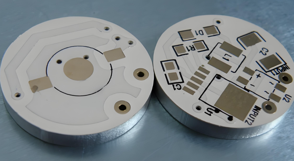
MCPCB technology also supports compact lighting designs. Because heat spreads more efficiently, engineers can place LEDs closer together without causing overheating problems.

FeatureAluminum PCBMCPCB
Core MaterialAluminumAluminum or copper
Thermal PerformanceHighVery high
CostModerateHigher
ApplicationsGeneral LED lightingHigh-power LED modules

Companies like EBest Circuit (Best Technology) manufacture high-precision MCPCB boards that support advanced LED lighting solutions across industries including automotive, architectural lighting, and industrial equipment.

LED Light Circuit Board – Aluminum & MCPCB for LED Lighting

What factors affect LED PCB performance?

The performance of an LED circuit board depends on multiple design and manufacturing factors. Even small variations in material quality or layout design can influence lighting efficiency and reliability. One major factor is thermal management. LEDs operate best when their junction temperature remains low. If heat cannot escape efficiently, performance may decline over time.

Another important factor is PCB material selection. Materials with higher thermal conductivity help transfer heat away from LEDs. Aluminum and metal core boards are widely used for this reason.

Several key elements influence LED PCB performance:

  • PCB substrate thermal conductivity
  • Copper trace thickness and layout
  • LED placement density
  • Quality of solder joints
  • Driver circuit design

Thermal vias and heat spreaders also play a major role in improving heat transfer. These design features allow heat to move from the top surface of the board to the metal base layer more efficiently.

Electrical stability is another important consideration. Proper circuit design ensures consistent current distribution across all LEDs. When current remains balanced, lighting output stays uniform and reliable. Manufacturing quality also affects performance. High-precision PCB fabrication reduces the risk of defects such as poor solder connections or uneven copper thickness.

Environmental conditions may also influence LED board reliability. Temperature fluctuations, humidity, and vibration can affect electronic components over time. Durable PCB materials and protective coatings help improve resistance to these environmental stresses.

Experienced manufacturers follow strict quality standards during production. Companies like EBest Circuit (Best Technology) apply advanced fabrication techniques and inspection processes to maintain consistent board performance.

How to make a circuit board for LED lights?

Designing and manufacturing a circuit board for LED lighting involves several steps. Each stage requires careful planning to ensure electrical stability and effective heat management.

The process usually begins with circuit design. Engineers determine the number of LEDs, their arrangement, and the electrical requirements of the lighting system. After the electrical schematic is complete, the layout design stage begins. Engineers create the physical arrangement of components and copper traces on the PCB.

The typical development process includes the following steps.

  • Define LED electrical requirements and power input
  • Create schematic diagrams for the circuit design
  • Design the PCB layout with proper trace routing
  • Select suitable PCB material such as aluminum or MCPCB
  • Manufacture the PCB through fabrication processes
  • Assemble LEDs and components using SMT or reflow soldering
  • Perform testing to confirm brightness and electrical stability

Thermal design is especially important during layout development. Engineers often place LEDs evenly across the board to distribute heat more effectively. Heat sinks may also be integrated into the final lighting product. These structures work together with the PCB to remove excess heat from the system.
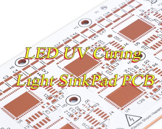
After assembly, the board undergoes testing procedures. Engineers check current distribution, brightness levels, and thermal behavior to confirm proper operation. If necessary, adjustments are made to improve performance before full production begins.

Working with experienced PCB manufacturers simplifies this process. Companies such as EBest Circuit (Best Technology) provide design support and fabrication services that help clients develop efficient LED lighting boards from concept to mass production.

How long do LED light boards last?

One of the biggest advantages of LED lighting technology is its long lifespan. When supported by a high-quality circuit board, LED light boards can operate for many years without significant performance loss.

Most LED lighting systems are designed to last between 30,000 and 50,000 hours of operation. Some advanced designs can even exceed this range when thermal management is optimized.

The circuit board plays a critical role in achieving this lifespan. Proper heat dissipation prevents excessive temperature buildup that could damage LED components. Several factors influence how long an LED board will last.

  • LED chip quality
  • Thermal conductivity of the PCB material
  • Operating temperature
  • Power driver stability
  • Environmental conditions

When these elements work together effectively, LED lighting products maintain stable brightness for a very long time.

Thermal management again proves essential. If the board transfers heat efficiently, the LED junction temperature stays within safe limits. This helps protect both the LEDs and surrounding electronic components. Manufacturers often perform accelerated life testing to evaluate long-term reliability. These tests simulate extended operation under controlled conditions to verify product durability.

Well-designed LED boards used in commercial lighting systems often remain functional for more than a decade in normal usage environments. High-quality production also improves longevity. Reliable solder joints, consistent copper thickness, and precise component placement all contribute to stable operation over time.

For this reason, many lighting brands work with specialized PCB manufacturers like EBest Circuit (Best Technology) that focus on quality control and durable board construction.

LED Light Circuit Board – Aluminum & MCPCB for LED Lighting

Where are LED light circuit boards commonly used?

LED light circuit boards appear in a wide range of modern lighting systems. Their compact design, high efficiency, and reliability make them suitable for many industries.

As LED technology continues to advance, the variety of applications keeps expanding. Some of the most common uses include:

  • Residential lighting such as bulbs, ceiling lights, and decorative lamps
  • Commercial lighting including office panels and retail lighting displays
  • Automotive lighting for headlights, signal lights, and interior illumination
  • Industrial lighting used in factories and warehouses
  • Outdoor lighting such as street lights and landscape illumination

LED boards are also widely used in electronic devices. Examples include televisions, display panels, gaming equipment, and smart home products. Architectural lighting is another growing application area. Designers often use LED boards to create flexible lighting solutions that highlight building structures and interior spaces.

Medical equipment, stage lighting, and emergency lighting systems also rely on LED circuit boards for stable and efficient illumination. The versatility of LED boards comes from their adaptable design. Engineers can customize board size, shape, and power level to match specific lighting requirements.

Companies like EBest Circuit (Best Technology) provide custom PCB manufacturing that supports these diverse applications. Our expertise helps clients develop reliable LED lighting modules tailored to different industries.

Summary:

LED light circuit boards form the core of modern LED lighting systems. They provide electrical pathways, structural support, and effective heat dissipation that allow LEDs to perform efficiently and reliably. Different PCB types, including FR4 boards, aluminum PCBs, and MCPCBs, serve various lighting needs. Among them, aluminum and metal core boards offer superior thermal performance for high-power lighting applications.
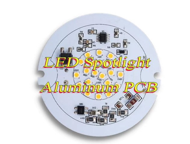
If you would like to learn more about LED PCB solutions or need customized circuit boards for your lighting products, feel free to contact EBest Circuit (Best Technology) for professional support. Contact: sales@bestpcbs.com

You may also like

Metal Core PCB Material | High Thermal Conductivity MCPCB Base Materials

March 6th, 2026

Electronic devices continue to shrink while power density keeps rising. Excess heat can shorten component life, reduce performance, and cause signal instability. Because of this, designers often select metal core PCB material instead of conventional laminates when thermal control becomes critical.
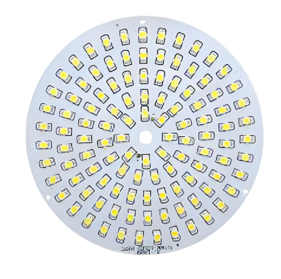
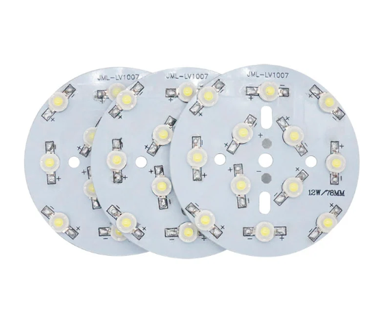
A metal core circuit board integrates a thermally conductive metal base beneath the dielectric and copper circuitry. This structure creates a direct path for heat to travel away from components. Compared with standard FR-4 boards, metal core PCBs can dissipate heat more efficiently and maintain better thermal balance during operation.

Metal Core PCB Material | High Thermal Conductivity MCPCB Base Materials

These boards are widely used in high-power LED lighting, automotive electronics, power converters, industrial control systems, and communication equipment. As power levels increase and device footprints shrink, engineers increasingly rely on aluminium core PCB, copper core PCB, and IMS PCB (Insulated Metal Substrate) technologies to stabilize thermal performance.

EBest Circuit (Best Technology)’s metal core PCB material provides excellent thermal conductivity, high stability and reliable performance for LED, power and high‑heat electronic applications.

What materials are used in metal core PCB?

A typical metal core PCB material structure consists of three primary layers. These layers work together to transfer heat efficiently from components to the metal substrate. Each layer performs a specific thermal and electrical function that ensures stable circuit performance.

The typical MCPCB stack structure includes:

  • Copper circuit layer
  • Thermal dielectric layer
  • Metal base layer

1. Copper Circuit Layer

The top layer contains copper traces that form the electrical circuit. This layer functions similarly to the copper layer in standard PCBs. Thicker copper improves current carrying capability and also spreads heat across the board surface. Copper thickness usually ranges from:

Copper ThicknessTypical Use
1 oz (35 μm)Standard LED and low-power circuits
2 oz (70 μm)Power LED modules
3 oz – 4 ozHigh-current power electronics

2. Thermal Dielectric Layer

The dielectric layer is a critical part of metal core PCB material. It electrically isolates the circuit from the metal base while still allowing heat to pass through. High thermal conductivity dielectric materials allow heat to move quickly from components into the metal base. Typical dielectric properties include:

PropertyTypical Range
Thermal conductivity1 W/mK – 10 W/mK
Thickness50 μm – 150 μm
Breakdown voltage2 kV – 6 kV

Common dielectric fillers include:

  • Ceramic particles
  • Aluminum oxide
  • Silicon compounds

These fillers increase thermal conductivity while maintaining insulation strength.

3. Metal Base Layer

The bottom layer of a pcb metal core acts as the primary heat sink. It spreads heat over a large surface area and transfers it to the external environment. Aluminum is widely used because it provides strong thermal performance at a reasonable cost. Copper offers the highest thermal conductivity but is heavier and more expensive. The most common base materials are:

Metal Base TypeThermal Conductivity
Aluminum~200 W/mK
Copper~385 W/mK
Steel~50 W/mK

How to choose metal core PCB material?

Selecting the right metal core pcb material depends on several engineering factors. The design must balance thermal performance, mechanical strength, electrical insulation, and manufacturing cost.

1. Thermal conductivity requirement

Heat dissipation is the main reason for using IMS PCB technology. The thermal conductivity of the dielectric layer determines how quickly heat moves into the metal base. Higher conductivity improves cooling performance. Typical ranges include:

Thermal ConductivityApplication
1–2 W/mKStandard LED lighting
3–5 W/mKAutomotive lighting
5–10 W/mKHigh-power electronics

2. Electrical insulation performance

Although the metal base conducts heat well, it must remain electrically isolated from the circuit layer. Reliable insulation prevents short circuits and protects sensitive components. Designers must verify:

  • Dielectric breakdown voltage
  • Insulation resistance
  • Long-term reliability under temperature cycling

3. Mechanical stability

Mechanical strength is also important when selecting metal core PCB materials. Aluminum substrates provide good rigidity while keeping board weight low. Copper base boards offer superior strength but increase overall board mass.

4. Manufacturing compatibility

Manufacturers evaluate whether the material supports standard processes such as:

  • SMT assembly
  • reflow soldering
  • drilling and routing
  • surface finishing

A stable material simplifies production and improves yield.

Metal Core PCB Material | High Thermal Conductivity MCPCB Base Materials

What material is the MCPCB made of?

An MCPCB (Metal Core Printed Circuit Board) typically combines three major materials: copper circuitry, thermal dielectric, and a metal substrate. However, within this structure, several variants exist depending on the application.

Aluminum Core PCB

An aluminium core PCB is the most widely used type of MCPCB. Aluminum offers excellent thermal conductivity while remaining lightweight and cost-effective. Typical aluminum grades used include:

  • 5052 aluminum
  • 6061 aluminum
  • 1060 aluminum

Advantages of aluminum core PCB include:

  • Lightweight structure
  • Good heat dissipation
  • Low material cost
  • Stable mechanical properties

Because of these benefits, aluminum core boards dominate LED lighting and power modules.

Copper Core PCB

A copper core PCB uses a solid copper substrate instead of aluminum. Copper has almost double the thermal conductivity of aluminum. This allows heat to move even faster away from components. However, copper boards are heavier and more expensive. Copper core PCBs are often used in:

  • high-power LEDs
  • RF power amplifiers
  • motor drivers
  • automotive electronics

IMS PCB (Insulated Metal Substrate)

An IMS PCB refers to a board where a dielectric layer isolates the circuit from the metal base. Most metal core PCBs fall into this category. The IMS structure allows designers to combine electrical insulation with thermal efficiency.

Typical IMS stack: Copper layer → thermal dielectric → aluminum base. This structure provides excellent heat dissipation while maintaining electrical isolation.

Metal Core PCB Material | High Thermal Conductivity MCPCB Base Materials

How thick is the metal core PCB?

The metal core pcb thickness varies depending on the design requirements. Engineers must consider both electrical performance and heat transfer efficiency. A typical MCPCB includes several thickness parameters.

Total board thickness. Thicker boards often improve mechanical strength. Common board thickness values include:

Board ThicknessApplication
1.0 mmThin LED modules
1.6 mmStandard MCPCB
2.0 mmHigh-power lighting
3.2 mmPower electronics

Metal core thickness. The metal base itself can vary significantly. A thicker metal base improves heat spreading capacity.

Metal Core ThicknessTypical Range
Aluminum base0.8 mm – 3.0 mm
Copper base1.0 mm – 4.0 mm

Dielectric thickness. The dielectric layer usually ranges between: 50 μm – 150 μm. A thinner dielectric improves thermal transfer but must still provide reliable electrical insulation.

Why is thermal conductivity important in metal core PCB material?

Thermal conductivity determines how quickly heat moves through a material. In electronic circuits, efficient heat removal protects components and stabilizes performance. High temperatures can reduce LED brightness, affect semiconductor switching speed, and shorten component lifespan.

A well-designed metal core PCB material structure solves this problem by creating a direct thermal path. Because the metal base spreads heat efficiently, the board avoids localized hot spots.

Heat flows through the following stages:

  • Component generates heat
  • Heat enters copper circuit layer
  • Heat moves through dielectric layer
  • Heat spreads across metal substrate
  • Heat dissipates into air or heat sink

Typical thermal conductivity comparison:

MaterialThermal Conductivity
FR-40.3 W/mK
Aluminum base~200 W/mK
Copper base~385 W/mK

What are benefits of metal core PCB material?

The advantages of metal core pcb materials extend beyond thermal performance. Engineers often select them because they improve reliability and design flexibility. Several benefits stand out. These advantages make pcb metal core technology suitable for high-power electronics.

  • 1. Excellent heat dissipation

Metal substrates rapidly transfer heat away from components. This reduces thermal stress and improves long-term reliability.

  • 2. Improved circuit stability

Stable temperatures keep semiconductor devices operating within their optimal range.

  • 3. High mechanical strength

Metal substrates increase board rigidity and durability.

  • 4. Compact product design

Efficient heat transfer allows designers to place components closer together.

  • 5. Longer product lifespan

Lower operating temperature helps protect LEDs, ICs, and power components.

  • 6. Reduced external cooling requirements

Many MCPCB designs operate without large heat sinks.

What is the difference between metal core PCB and FR4?

A metal core PCB vs FR4 comparison highlights the fundamental differences between the two technologies.

FR-4 is a fiberglass epoxy laminate commonly used in conventional PCBs. While it offers good electrical insulation, it has limited thermal conductivity. Metal core boards replace the fiberglass base with a thermally conductive metal substrate. In applications with high power density, metal core circuit boards offer clear advantages.

Below is a comparison of the two materials.

FeatureMetal Core PCBFR-4 PCB
Base materialAluminum or copperGlass fiber epoxy
Thermal conductivityHighLow
Heat dissipationExcellentLimited
Mechanical strengthStrongModerate
WeightHeavierLightweight
Typical applicationsLEDs, power electronicsConsumer electronics
Metal Core PCB Material | High Thermal Conductivity MCPCB Base Materials

Where is metal core PCB material used?

Because of its thermal advantages, metal core PCB material appears in many modern electronic systems. Industries rely on MCPCBs to manage heat in compact designs. Common applications include:

LED lighting, High-power LEDs generate substantial heat. MCPCBs help maintain consistent brightness and extend LED life.

Examples include:

  • street lighting
  • automotive headlights
  • industrial lighting

Automotive electronics, Vehicles require reliable thermal management for components such as:

  • engine control modules
  • power converters
  • lighting systems

Power electronics, Power supplies and converters generate high heat density. Metal core boards stabilize thermal performance in:

  • motor drives
  • DC-DC converters
  • industrial power modules

Communication systems, RF amplifiers and communication equipment often use copper core PCB structures to dissipate heat from power devices.

Consumer electronics, Compact devices such as projectors and audio equipment also benefit from MCPCB technology.

At EBest Circuit (Best Technology), we specialize in manufacturing high-quality metal core PCBs and thermal management circuit boards for demanding applications. Our engineering team supports customers from design review to production, ensuring each board meets strict performance standards.

If you are developing high-power electronic products and need reliable metal core PCB materials, feel free to contact our team. Email: sales@bestpcbs.com

You may also like

PCB Thermal Conductivity Guide: Materials, Heat Dissipation & Thermal Design

March 5th, 2026

If you work with electronic devices, you’ve probably heard of PCB thermal conductivity. But do you know what it really means? Or why it matters for your projects? This guide breaks down everything you need to know—from key materials to design tips

What Is PCB Thermal Conductivity?

PCB thermal conductivity refers to the ability of a printed circuit board material to transfer heat from one location to another. It is typically measured in W/m·K (Watts per meter-Kelvin).

A higher thermal conductivity value means heat travels more efficiently through the board. This helps prevent local hot spots and keeps electronic components operating within safe temperature limits.

Electronic components generate heat during operation. If the PCB cannot dissipate this heat effectively, several problems may occur:

  • Component overheating
  • Reduced electrical performance
  • Accelerated material aging
  • Solder joint fatigue
  • Unexpected system failure

Because of these risks, thermal performance is now a critical parameter in PCB design.

What Is PCB Thermal Conductivity?

What Is PCB Thermal Conductivity?

Why Thermal Conductivity is Important in PCB?

Thermal conductivity becomes especially important in systems such as:

  • LED lighting modules
  • automotive power electronics
  • RF communication equipment
  • industrial motor controllers
  • high-density computing hardware

In these systems, components like MOSFETs, power regulators, and RF amplifiers can generate significant heat during operation. A properly designed PCB spreads that heat efficiently across copper planes and into external cooling systems.

Thermal Conductivity of Common PCB Materials

Different PCB materials conduct heat at different rates. The base laminate, metal layers, and structural design all influence overall thermal performance.

The following table shows typical thermal conductivity values for common PCB materials.

PCB MaterialThermal Conductivity (W/m·K)Typical Applications
FR-4 Standard Laminate0.3 – 0.4Consumer electronics
High-Tg FR-40.4 – 0.6Industrial electronics
Aluminum PCB1 – 3LED lighting, power modules
Copper~385Heat spreading layer
Ceramic (Alumina)20 – 30RF modules, high-power circuits
Aluminum Nitride (AlN)140 – 180High-power semiconductor modules

Most standard PCBs use FR-4 epoxy glass laminate. While FR-4 is cost-effective and electrically stable, its thermal conductivity is relatively low. This is why designers often rely on copper planes and thermal vias to improve heat flow.

Which PCB Material Has the Highest Thermal Conductivity?

Among commonly used PCB materials, ceramic substrates offer the highest thermal conductivity.

Aluminum nitride (AlN) stands out because it combines high thermal conductivity with excellent electrical insulation. Its thermal conductivity can exceed 170 W/m·K, which is hundreds of times higher than standard FR-4. Despite its excellent thermal properties, AlN is significantly more expensive than FR-4. Manufacturing complexity is also higher.

Therefore, ceramic PCBs are usually reserved for applications that require extreme thermal performance, such as:

  • power semiconductor modules
  • high-frequency RF systems
  • aerospace electronics
  • high-power laser drivers

For most industrial products, aluminum PCB or optimized FR-4 stack-ups provide sufficient thermal performance at a more reasonable cost.

How Does Copper Thickness Affect PCB Thermal Conductivity?

Copper plays a major role in PCB heat spreading. Although the base laminate may have low thermal conductivity, copper traces and planes help move heat away from components. Copper has a thermal conductivity of approximately 385 W/m·K, which is extremely high compared with FR-4.

Increasing copper thickness improves thermal performance in several ways:

  1. Thicker copper spreads heat across a larger area.
  2. Reduced resistance helps decrease power loss.
  3. Heat moves more evenly through copper planes.

Typical PCB copper thickness values include:

Copper WeightThickness
1 oz~35 µm
2 oz~70 µm
3 oz~105 µm
4 oz~140 µm

Power electronics designs often use 2 oz or thicker copper. Heavy copper PCBs can reach 6 oz or even higher for extreme current applications. However, thicker copper also introduces design considerations:

  • trace spacing requirements increase
  • etching becomes more challenging
  • manufacturing cost rises

Therefore, engineers usually balance copper thickness with other thermal management methods such as thermal vias and heat sinks.

How Can You Improve PCB Thermal Conductivity in Design?

Even when using standard FR-4 materials, designers can significantly improve heat dissipation through thoughtful PCB layout and structure. Several design techniques are commonly used.

1. Use Larger Copper Planes

Copper planes distribute heat across the board surface, you can use large ground planes or power planes act as heat spreaders.

2. Add Thermal Vias

Thermal vias create vertical heat paths between layers. They allow heat to move from the component side to inner copper planes or heat sinks.

3. Select Metal Core PCB

Metal core PCBs use aluminum or copper substrates. These materials improve thermal conductivity and enable efficient heat transfer.

4. Optimize Component Placement

Components that generate significant heat should not be crowded together. Proper spacing helps air circulation and reduces temperature buildup.

5. Use Heat Sinks

External heat sinks remove heat from the PCB and release it into the surrounding environment.

What Is the Difference Between Thermal Conductivity and Thermal Resistance in PCB?

Thermal conductivity and thermal resistance are related but different concepts.

  • Thermal conductivity describes how well a material conducts heat.
  • Thermal resistance measures how difficult it is for heat to travel through a structure.

The relationship can be expressed as:

Thermal Resistance = Thickness / (Thermal Conductivity × Area)

In PCB design, this means:

  • thicker materials increase thermal resistance
  • higher conductivity materials reduce resistance
  • larger heat transfer areas improve cooling

Designers often calculate thermal resistance when evaluating cooling performance. A lower thermal resistance means heat can flow away from components more easily.

Where Are High Thermal Conductivity PCBs Used?

High thermal conductivity PCBs appear in many modern electronic systems. As power density increases, thermal design becomes more critical.

Common applications include:

  • LED lighting systems
  • automotive control modules
  • power converters and inverters
  • telecom base stations
  • RF amplifiers
  • industrial automation equipment

Similarly, power electronics used in electric vehicles require efficient thermal management. Heavy copper PCBs and thermal vias help maintain stable operating temperatures. In RF systems, excessive heat can affect signal stability, thermal control therefore supports both reliability and electrical performance.

Why Choose EBest as Your High Thermal Conductivity PCB Manufacturer?

At EBest Circuit (Best Technology), we focus on supporting engineers who require reliable PCB fabrication and assembly solutions for high-performance electronics. Our team has over 19 of experience in PCB and PCBA manufacturing. Our facilities operate in both China and Vietnam, allowing us to support global supply chains and flexible production requirements.

We work closely with customers during the early engineering stage. Our engineering team reviews design files and provides practical DFM feedback that helps improve manufacturability and thermal performance.

Our capabilities include:

  • multilayer PCB fabrication up to complex stack-ups
  • aluminum PCB and metal core PCB manufacturing
  • heavy copper PCB production
  • thermal via drilling and filling technologies
  • SMT and THT assembly services
  • component sourcing and turnkey PCBA

For PCB fabrication, thermal design consultation, or turnkey PCBA services, feel free to contact our team at sales@bestpcbs.com.

FAQ About PCB Thermal Conductivity

1. How can I improve PCB heat dissipation?

    Several design methods improve PCB heat dissipation. Common techniques include:

    • using thicker copper layers
    • adding thermal vias
    • increasing copper plane area
    • selecting aluminum PCB substrates
    • attaching external heat sinks

    2. What PCB material is best for thermal management?

    Ceramic materials such as aluminum nitride offer the highest thermal conductivity. However, aluminum PCBs provide an excellent balance between cost and performance. Many LED and power electronics systems use aluminum substrates. For general applications, optimized FR-4 with thermal vias can also deliver effective thermal management.

    3. Does thicker copper improve thermal conductivity?

    Yes. Thicker copper improves heat spreading across the board. Copper conducts heat extremely well. Increasing copper thickness creates larger thermal paths that help distribute heat more evenly.

    4. Is aluminum PCB better for heat dissipation?

    Yes. Aluminum PCBs provide significantly better heat dissipation than standard FR-4 boards.

    The aluminum base acts as a heat spreader and transfers heat quickly to external cooling systems.

    You may also like

    Amplifier PCB Circuit | High-Fidelity Low-Noise Audio PCB Design

    February 3rd, 2026

    Need professional amplifier PCB circuit design? We provide optimized PCB circuit solutions with precise wiring and impedance matching for high-performance audio amplifiers. Get custom quote here.

    Amplifier PCB Circuit | High-Fidelity Low-Noise Audio PCB Design

    What Is a PCB in an Amplifier?

    PCB in an amplifier is the physical platform that connects and supports all electronic parts required to boost an audio signal. It holds active devices such as transistors or ICs, passive parts like resistors and capacitors, and power components that deliver current to the load.

    In an audio amplifier, the PCB does far more than provide mechanical support. It controls impedance, limits interference, and manages heat. From a functional view, an amplifier PCB usually integrates several blocks. These blocks work together on the same board.

    Input traces handle tiny signals and need isolation. Output paths carry high current and need wide copper and short routes. The PCB ties these together in a controlled and repeatable way.

    What Are the Different Types of Amplifier PCBs?

    Amplifier PCBs vary based on function, power level, and application environment. There is no single universal board style. One common way to classify amplifier PCB circuits is by amplifier class.

    • Class A amplifier PCBs favor simplicity and linearity. They generate constant heat and require strong thermal paths.
    • Class AB amplifier PCBs balance efficiency and sound quality. They need careful bias routing and stable grounding.
    • Class D amplifier PCBs switch at high frequency. They demand controlled impedance, tight loop areas, and EMI control.

    Another way to group amplifier PCBs is by construction style.

    • Single-layer PCBs appear in low-cost or simple amplifier modules. They are easy to make but limited in performance.
    • Double-layer PCBs are common in consumer audio. They allow better grounding and signal routing.
    • Multilayer PCBs support high-end or compact amplifiers. Dedicated ground and power planes improve noise control.
    • Metal-core PCBs help in power amplifiers where heat dissipation is critical.
    • Rigid-flex PCBs appear in space-constrained or portable audio devices.

    Application also influences PCB type. A headphone amplifier PCB looks very different from a 1000-watt PA amplifier PCB. Automotive and industrial amplifiers may need thicker copper, higher Tg materials, or special surface finishes to handle stress.

    At EBest Circuit (Best Technology), amplifier PCB projects often range from compact low-noise audio boards to heavy-copper power amplifier PCBs. The board type is selected after reviewing power level, thermal load, and target market.

    How Are Amplifier PCB Circuit Design?

    • The first step is schematic planning. Once the schematic is stable, PCB design translates theory into copper.
    • Signal integrity is always a priority. Low-level input signals must be protected from noise sources. These traces should be short, direct, and shielded by ground when possible.
    • Thermal design is another core concern. Output devices and regulators generate heat. The PCB must spread this heat through copper pours, thermal vias, or metal substrates.
    • Power distribution must be stable. Decoupling capacitors should sit close to active devices. Bulk capacitors need short return paths.

    Key layout practices include:

    • Keeping high-current loops small
    • Separating signal and power sections
    • Using wide copper for output stages
    • Placing feedback paths carefully
    • Controlling trace impedance in Class D designs

    Amplifier PCB circuit design is not only about rules. It also involves experience. Manufacturers like EBest Circuit (Best Technology) often support customers with design feedback, pointing out layout risks before production. That early review saves time and cost later.

    Amplifier PCB Circuit | High-Fidelity Low-Noise Audio PCB Design

    The Manufacturing Process of a Custom Amplifier PCB Circuit

    Once an amplifier PCB circuit design is finalized, manufacturing turns digital files into a physical board. Most audio amplifier PCBs use FR-4, but high-power or high-temperature designs may need high-Tg laminates or metal-core substrates. Copper thickness is chosen based on current load.

    The typical manufacturing flow includes several stages.

    • Data preparation, where Gerber files and drill data are checked
    • Inner layer imaging, for multilayer boards
    • Lamination, bonding layers under heat and pressure
    • Drilling, creating vias and mounting holes
    • Plating, adding copper to holes and surfaces
    • Outer layer imaging and etching, forming final traces
    • Solder mask application, protecting copper and defining pads
    • Surface finish, such as ENIG or HASL
    • Electrical testing, verifying connectivity

    For amplifier PCBs, quality control is critical. Trace width tolerance affects impedance and current capacity. Via quality affects thermal transfer. Solder mask accuracy affects assembly yield.

    Custom amplifier PCB circuits often need tighter inspection than standard digital boards. Audio customers expect low noise and long service life.

    EBest Circuit (Best Technology) integrates PCB fabrication with PCBA services, allowing amplifier boards to move smoothly from bare board to assembled unit. That integration reduces handling risk and shortens delivery cycles.

    What Are the Advantages of Amplifier PCBs?

    Amplifier PCBs offer clear benefits compared to loose wiring or ad-hoc construction.

    • One major benefit is electrical stability. A PCB enforces consistent trace lengths and grounding paths.
    • Another advantage is compact size. PCBs allow dense placement of parts without sacrificing performance.
    • Reliability also improves with PCBs. Fixed copper traces do not loosen like wires.

    Key advantages include:

    • Lower noise through controlled grounding
    • Better heat management with copper pours
    • Higher assembly efficiency
    • Easier troubleshooting and repair
    • Scalable production from prototype to volume

    Amplifier PCBs also support modern compliance needs. They allow traceability, automated inspection, and standardized testing.

    How Does an Amplifier PCB Circuit Work in Audio Amplifier Systems?

    An amplifier PCB circuit works by guiding an audio signal through a controlled amplification path while supplying power and maintaining stability. The PCB does not amplify by itself, but it enables each component to do its job correctly.

    • The process begins at the input. The PCB routes the incoming signal to the first gain stage. This area must stay quiet.
    • Next comes voltage amplification. Transistors or ICs increase signal amplitude. The PCB ensures that feedback paths remain stable and short.
    • The output stage then delivers current to the load. This part of the PCB handles high current and heat. Wide traces, thick copper, and solid ground returns are common.
    • Throughout the circuit, the power supply section feeds clean voltage. Decoupling capacitors smooth fluctuations. The PCB keeps these loops tight to prevent ripple and noise from leaking into the signal path.
    • Protection circuits often sit near the output. They monitor temperature, current, or DC offset. The PCB must connect these accurately to respond fast in fault conditions.

    In a complete audio amplifier system, the PCB acts as the nervous system. It coordinates signal flow, power delivery, and protection.

    Amplifier PCB Circuit | High-Fidelity Low-Noise Audio PCB Design

    What Are the Applications of Amplifier PCBs?

    Amplifier PCBs appear in many products, far beyond traditional home audio. Any system that needs to boost a signal relies on some form of amplifier circuit PCB.

    Common application areas include:

    • Home audio amplifiers and receivers
    • Professional sound systems and mixers
    • Automotive audio and infotainment
    • Headphone amplifiers and DACs
    • Musical instrument amplifiers
    • Public address systems
    • Industrial signal amplification
    • Medical and measurement equipment

    Each application places different demands on the amplifier PCB circuit. Home audio focuses on low noise and clean sound. Automotive amplifiers need vibration resistance and temperature tolerance. Industrial systems demand long-term stability.

    EBest Circuit (Best Technology) works with customers across these sectors, supporting both low-volume prototypes and stable mass production.

    How to Choose a Custom Amplifier PCB Circuit Supplier?

    Choosing the right supplier for an amplifier PCB circuit is a strategic decision. The supplier influences performance, cost, delivery, and long-term reliability.

    • Technical capability should come first. The supplier must understand audio-specific challenges such as noise control, thermal design, and high-current routing.
    • Manufacturing range also matters. A good supplier supports different board types, copper weights, and finishes.
    • Quality systems are another key factor. Certifications, inspection methods, and traceability protect your product reputation.
    • Communication style matters more than many expect. Amplifier PCB projects often evolve during prototyping.

    When evaluating suppliers, consider these points:

    • Experience with amplifier PCB circuits
    • Support for DFM and layout review
    • Stable material sourcing
    • Clear quality control process
    • Ability to scale from prototype to volume

    EBest Circuit (Best Technology) positions itself as a one-stop PCB and PCBA partner. By combining fabrication and assembly, it helps audio amplifier projects move faster with fewer handoffs.

    Amplifier PCB Circuit | High-Fidelity Low-Noise Audio PCB Design

    Conclusion:

    An amplifier PCB circuit is the foundation of audio amplifier performance. It shapes signal integrity, controls noise, manages heat, and ensures consistency from unit to unit. From basic input routing to high-current output stages, every layout decision affects sound quality and reliability.

    If you are developing a custom amplifier PCB circuit and want a partner who understands audio requirements, manufacturing precision, and scalable production, EBest Circuit (Best Technology) can support your project from concept to delivery.

    For technical consultation or a quotation, please contact sales@bestpcbs.com

    You may also like

    Why Ink Blistering Failures Occurs on Thermally conductive PCBs?

    February 2nd, 2026

    If you design or manufacture high-power electronics—such as LED modules, automotive electronics, or power supplies—you have likely encountered a costly issue: solder mask ink blistering or peeling on thermally conductive, copper-based PCBs.

    This defect is far more than cosmetic. Once the ink detaches, insulation is compromised, copper is exposed, and the risk of corrosion, short circuits, and field failures increases sharply. The question is not if it can happen, but why it happens so often on thermally conductive PCBs—and how to prevent it in a controlled, repeatable way.

    This guide explains the real root causes and provides a practical, engineering-driven prevention strategy.

    Why Do Thermally Conductive PCBs Suffer from Ink Blistering?

    Thermally conductive PCBs are designed to dissipate heat efficiently, often using thick copper layers, metal cores, or high-performance dielectric materials. These features make them excellent thermal performers—but also introduce mechanical stress.

    The core issue is CTE mismatch. Copper, dielectric layers, substrates, and solder mask ink all expand and contract at different rates when exposed to heat. During soldering and thermal cycling, this mismatch generates strong shear forces at the ink-to-copper interface.

    When stress exceeds adhesion strength, failure occurs. The ink does not fail randomly—the bond fails at its weakest point.

    Why Do Thermally Conductive PCBs Suffer from Ink Blistering?

    What Actually Fails When Ink Blisters or Peels Off?

    The final failure mode is always the same: loss of adhesion between the solder mask ink and the copper surface.

    Once this bond weakens:

    • Heat causes localized lifting
    • Trapped moisture expands into vapor
    • Flux chemicals penetrate the interface
    • The ink blisters, cracks, or peels away

    Understanding why adhesion weakens is the key to long-term prevention.

    Why Does Ink Adhesion Fail on Thermally Conductive PCBs?

    Ink adhesion failure is rarely caused by a single factor. In most cases, it is the result of multiple small weaknesses stacking together.

    1. Poor Surface Preparation

    This is the most common root cause. Any contamination—oxide layers, oils from handling, dust, or residual plating chemicals—prevents proper bonding. Even a surface that is too smooth can be a problem, as the ink has nothing to mechanically anchor to.

    Moisture trapped in vias or micro-voids becomes steam during soldering, pushing the ink away from underneath.

    2. Using the Wrong Type of Ink

    Standard solder masks developed for FR-4 are not designed for metal-core or high-thermal-conductivity boards. Their mechanical flexibility and thermal resistance are insufficient for the stress environment.

    Expired ink or ink stored outside recommended conditions further degrades adhesion performance.

    3. Incomplete or Incorrect Curing

    Ink that is not fully cured remains chemically weak. Fast ramp rates, uneven oven temperatures, or insufficient soak time prevent full polymer cross-linking.

    Visually, the ink may look acceptable—but internally, it lacks structural strength.

    4. Chemical Attack During Assembly

    Highly active fluxes can migrate under poorly bonded ink edges. Under reflow temperatures, these chemicals aggressively attack the interface, triggering sudden blistering or peeling after assembly.

    5. Design-Driven Thermal Stress

    Large copper pours and thick copper planes act as stress concentrators. Repeated thermal cycling during soldering, testing, and operation gradually fatigues the ink bond in these high-stress zones.

    How Can Surface Preparation Be Optimized for Ink Adhesion?

    The goal of surface preparation is simple: clean, micro-roughened, and moisture-free copper.

    Key actions include:

    • Using controlled acidic cleaning followed by high-pressure DI water rinsing
    • Applying chemical micro-etch or plasma treatment to achieve Ra 0.4–0.8 µm
    • Enforcing a strict “print within 2 hours” window after surface treatment
    • Avoiding manual handling after preparation

    Surface preparation sets the foundation. If this step fails, no ink can compensate.

    How Should Ink Be Selected and Handled for These Boards?

    Ink selection must match the application environment.

    Best practices include:

    • Using solder mask inks specifically qualified for metal-core or high-thermal PCBs
    • Reviewing technical data sheets and Certificates of Analysis
    • Storing ink at controlled temperature and humidity
    • Enforcing FIFO inventory and never using expired material

    Ink should be treated as a critical chemical, not a consumable.

    What Printing and Curing Controls Prevent Ink Failures?

    Printing and curing are where most hidden failures originate.

    To maintain consistency:

    • Control ink viscosity using a viscometer
    • Measure dried ink thickness regularly (typically 25–35 µm)
    • Ensure uniform coverage across thick copper areas
    • Profile curing ovens using actual board measurements

    Curing must follow the ink supplier’s recommended ramp-and-soak profile exactly. Assumptions are not acceptable—verification is required.

    What Printing and Curing Controls Prevent Ink Failures?

    How Can Ink Reliability Be Validated Before Shipment?

    Validation should simulate real assembly and field conditions.

    Recommended tests include:

    • Cross-hatch tape adhesion testing (IPC-TM-650 2.4.28)
    • 288°C solder float testing
    • Multiple simulated reflow cycles
    • Compatibility testing with selected solder pastes and fluxes

    If ink survives these tests, it is far more likely to survive real use.

    How Can PCB Design Reduce Ink Stress and Blistering Risk?

    Design choices strongly influence ink reliability.

    Effective DFM measures include:

    • Using rounded corners on large copper pours
    • Adding solder mask anchor features where possible
    • Avoiding abrupt copper thickness transitions
    • Communicating ink and assembly risks early in design reviews

    Design collaboration prevents problems that manufacturing alone cannot fix.

    Why Is Pre-Bake Important Before Assembly?

    Moisture is a silent contributor to blistering.

    Pre-baking boards at 125°C for 1–2 hours before assembly removes absorbed moisture from substrates and vias. This simple step dramatically reduces steam-induced ink lifting during reflow.

    Why Is Pre-Bake Important Before Assembly?

    How Should Ink Blistering Be Troubleshot Systematically?

    When failures occur, follow a structured approach:

    1. Observe the blistering pattern
    2. Large, uniform blistering usually points to curing or ink issues
    3. Localized blistering often indicates contamination or handling problems
    4. Failures only after soldering suggest incomplete cure or flux attack

    Systematic analysis saves time and prevents repeated mistakes.

    What Is the Key to Preventing Ink Blistering Long Term?

    Ink blistering on thermally conductive PCBs is not random. It is the result of unmanaged stress and weak process control.

    Prevention comes from:

    • Proper material selection
    • Controlled surface preparation
    • Verified curing processes
    • Design collaboration
    • Assembly compatibility planning

    When these elements are managed together, ink blistering becomes a rare exception rather than a recurring problem.

    Ready to Eliminate Ink Blistering on Thermally Conductive PCBs?

    Ink blistering and solder mask peeling are not inevitable problems—they are signals that something in material selection, process control, or design collaboration needs to be improved.

    If you are working with thermally conductive, copper-based, or metal-core PCBs and want to prevent ink failures before they reach assembly or the field, working with an experienced manufacturing partner makes a measurable difference.

    At EBest Circuit, we support engineers with:

    • Early DFM and process risk review for thermally conductive PCBs
    • Proven solder mask and surface treatment processes for high-thermal designs
    • Full PCB + PCBA one-stop service, including testing and traceability
    • Prototype and small-volume support with fast technical feedback

    If you’d like a second opinion on your board design, process flow, or ink-related reliability risks, feel free to contact our engineering team.

    📩 Email: sales@bestpcbs.com

    We’re here to help you turn thermal performance into long-term reliability—without surprises after reflow.

    You may also like

    PCB Manufacturer in Dubai

    December 24th, 2025

    Looking for PCB manufacturer in Dubai? This comprehensive guide outlines top providers, key selection criteria, and solutions to common manufacturing pain points.

    Dubai’s position as a global technological and industrial hub has fostered a dynamic ecosystem of PCB manufacturer in Dubai, catering to diverse sectors from aerospace to consumer electronics. For those seeking reliable partners in this region, understanding the PCB manufacturer in Dubai is crucial to making informed decisions that align with project requirements and quality standards. This guide delves into the key players, core challenges, and evaluation frameworks for PCB manufacturer in Dubai, offering actionable insights to navigate the local market effectively and secure supply chain stability.

    PCB Manufacturer in Dubai, https://www.bestpcbs.com/blog/2025/12/pcb-manufacturer-in-dubai/

    Top 10 PCB Manufacturer in Dubai

    Company NameCore Business AdvantagesKey StrengthsManufacturing CapabilitiesLead Time
    EBest Circuit (Best Technology) Co.,LtdOne-stop PCB design, prototyping, manufacturing & assembly; automotive and aerospace PCB solutions19+ years of industry experience; ISO9001/ISO13485/IATF16949 certified; 97.2% on-time delivery rate1-16 layer rigid-flex PCBs; 0.1mm laser drilling; heavy copper PCBs (up to 6oz); impedance control ±5%; ceramic & FR4 materials24 hours for 2-layer prototypes; 7-12 days for mass production
    Falcon ElectronicsPCB assembly & prototyping; automotive and consumer electronics-focused OEM servicesEstablished in 2008; ISO certified; Dubai Silicon Oasis location for logistical advantage2-12 layer PCBs; SMT & through-hole assembly; rigid PCB fabrication; IPC-6012 compliant5-7 days for prototypes; 10-15 days for mass production
    Precision Electronics UAEHigh-quality PCB fabrication; rapid prototyping; small to medium volume production12+ years of local experience; client-recommended for precision; Dubai Investment Park base1-8 layer PCBs; laser direct imaging (LDI) technology; FR4 & aluminum-based materials; AOI inspection3-5 days for prototypes; 8-12 days for mass production
    Globaltronics Manufacturing L.L.C.Contract electronics manufacturing; PCB assembly for telecom, defense & industrial sectorsJebel Ali Free Zone location; multiple ISO certifications; lean manufacturing processes2-16 layer PCBs; HDI boards; SMT & MID technologies; RoHS compliant materials6-8 days for prototypes; 12-18 days for mass production
    Naoki Design SolutionsRigid PCB fabrication; prototype & production services; local technical supportBur Dubai location; specialized in FR4 materials; tailored solutions for local industries2-20 layer rigid PCBs; vacuum etching; line width/spacing 3/3 mil; interlayer alignment ≤25μm4-6 days for prototypes; 9-14 days for mass production
    Popular ElectronicsPrinted circuit board supply; electronic components; technical equipment maintenanceDeira & Nad Al Hamar locations; established local distribution network; quick response service1-6 layer PCBs; glass-reinforced plastic substrates; standard surface treatments (OSP, HASL)3-7 days for prototypes; 10-15 days for mass production
    Emirates Electronics Factory (Dubai Branch)Turnkey electronics manufacturing; PCB assembly; full product assembly services15+ years of UAE market experience; international quality standard compliance; scalable production2-14 layer PCBs; SMT assembly; through-hole technology; environmental testing support7-10 days for prototypes; 14-20 days for mass production
    Techno Print Circuits DubaiCustom PCB fabrication; high-frequency PCBs; industrial electronics solutionsSpecialized in high-temperature materials (TG 180-220℃); advanced process control2-18 layer PCBs; high-frequency microwave PCBs; impedance control ±5%; laser drilling5-8 days for prototypes; 12-16 days for mass production
    Dubai Electronic Manufacturing Co.PCB prototyping & production; electronic assembly; quality testing servicesIndustrial zone location; modern production facility; strict quality assurance protocols1-10 layer PCBs; FR4 & CEM materials; AOI & flying probe testing; copper thickness uniformity ±1.5μm4-6 days for prototypes; 9-13 days for mass production
    Smart Circuit Technologies DubaiHDI PCB manufacturing; rigid-flex solutions; IoT device PCB componentsFocus on smart city applications; innovative micro-via technology; quick-turn services4-16 layer HDI PCBs; rigid-flex PCBs; 0.1mm micro-vias; ENIG surface treatment6-9 days for prototypes; 13-17 days for mass production

    How to Choose A Reliable PCB Manufacturer in Dubai?

    Selection Guide to PCB Manufacturer in Dubai:

    • Validate industry certifications and compliance with international standards (ISO 9001, IPC-A-600G, RoHS): These certifications serve as critical benchmarks for ensuring your PCB designs meet global quality requirements and regulatory mandates, reducing risks of non-compliance in end-product markets.
    • Align manufacturer’s process capabilities with your design specifications: Evaluate if the manufacturer can accommodate your project’s unique requirements, such as layer count, fine line width/spacing (e.g., 2/2 mil for HDI designs), and compatibility with specialized materials like high-frequency or ruggedized substrates.
    • Assess on-time delivery track record and flexibility for time-sensitive projects: Review historical on-time delivery data, and confirm the manufacturer can handle expedited orders or adapt to last-minute design adjustments without compromising production quality, which is vital for maintaining your project timelines.
    • Scrutinize quality control (QC) processes and inspection capabilities: Verify the manufacturer employs advanced QC technologies (AOI, flying probe testing, X-ray inspection) and has a transparent defect rate history, ensuring potential design or production flaws are detected early in the manufacturing cycle.
    • Evaluate local supply chain integration and logistics efficiency: A manufacturer with robust local supply chain links and proximity to Dubai’s key ports/airports can minimize lead times, reduce transportation risks, and ensure timely delivery of materials and finished PCBs for your global projects.
    • Gauge technical support and engineering collaboration capacity: Prioritize manufacturers that offer proactive technical support for complex or custom designs, such as early-stage design for manufacturability (DFM) reviews, to optimize your designs and avoid production bottlenecks.
    • Compare pricing structures and value-added services: Look beyond base costs to assess cost-effectiveness, including value-added services like rapid prototyping, design optimization, and post-production support, ensuring you get quality results without unnecessary expenses.
    • Check customer references and industry reputation: Seek feedback from peers in your sector (e.g., automotive, aerospace, telecom) to evaluate the manufacturer’s performance with similar designs, as well as the reliability of their after-sales support for issues like design iterations or quality follow-ups.
    How to Choose A Reliable PCB Manufacturer in Dubai, https://www.bestpcbs.com/blog/2025/12/pcb-manufacturer-in-dubai/

    Core Pain Points of PCB Manufacturer in Dubai

    • Heavy reliance on imported raw materials (copper, FR4 substrates, specialty alloys), leading to supply chain volatility and cost fluctuations​.
    • Shortage of skilled technical personnel, particularly in high-precision processes like HDI board fabrication and impedance control​.
    • Stringent environmental regulations on electronic waste management, increasing production and disposal costs​.
    • Intense competition from international PCB manufacturers supplying the Dubai market, pressuring local pricing and profit margins​.
    • Limited local R&D capabilities for advanced PCB technologies, hindering innovation in high-frequency and automotive-grade products​.
    • Fluctuating energy costs in Dubai, impacting the energy-intensive PCB manufacturing processes (etching, plating, curing)​.
    • Challenges in meeting the growing demand for small-batch and custom PCB orders due to rigid production line configurations​.
    • Delays in customs clearance for imported equipment and materials, disrupting production schedules and lead times.

    How to Evaluate Production Capacity of PCB Manufacturer in Dubai?

    Evaluation Guide to Production Capacity of PCB Manufacturer in Dubai:

    • Review monthly production volume capabilities and current order saturation to ensure capacity for your requirements​.
    • Inspect manufacturing facilities and equipment, including automation level and advanced machinery (e.g., LDI exposure machines, vacuum etching lines)​.
    • Assess scalability by evaluating the manufacturer’s ability to ramp up production volumes within required timelines.​
    • Verify raw material inventory management and supply chain resilience to avoid production delays due to material shortages​.
    • Evaluate multi-shift operation capabilities to meet tight deadlines or high-volume demands​.
    • Review process diversification, including the ability to handle different PCB types (rigid, flexible, HDI) and technologies​.
    • Analyze historical production data for on-time completion rates and capacity utilization during peak periods​.
    • Assess the manufacturer’s engineering team size and expertise to support production optimization and problem-solving.

    How to Evaluate Delivery Time of PCB Manufacturing Company Dubai?

    Evaluation Guide to Delivery Time of PCB Manufacturer in Dubai:

    • Confirm standard lead times for different order types (prototype, low-volume, high-volume) and compare against industry benchmarks​.
    • Evaluate expedited service options and associated costs for time-sensitive projects​.
    • Review production scheduling processes and flexibility to accommodate last-minute design changes or order adjustments​.
    • Assess logistics and shipping capabilities, including proximity to ports/airports and partnerships with reliable logistics providers​.
    • Verify inventory management systems for critical raw materials to minimize delays from material procurement​.
    • Evaluate the manufacturer’s track record for on-time delivery through customer references and performance reports​.
    • Assess contingency plans for production disruptions (e.g., equipment failure, supply chain issues) that could impact delivery​.
    • Confirm clear communication protocols for delivery status updates and potential delay notifications.
    How to Evaluate Delivery Time of PCB Manufacturing Company Dubai, https://www.bestpcbs.com/blog/2025/12/pcb-manufacturer-in-dubai/

    How to Inspect Quality Control Processes of PCB Manufacturing Company Dubai?

    Inspection Guide to Quality Control Processes of PCB Manufacturing Company Dubai:

    • Verify the presence of a comprehensive quality management system (QMS) certified to ISO 9001 or relevant industry standards​.
    • Inspect incoming material inspection (IQC) processes for raw material verification and compliance with specifications​.
    • Evaluate in-process quality control (IPQC) measures, including real-time monitoring of critical production parameters​.
    • Review outgoing quality control (OQC) procedures, including final inspection technologies (AOI, flying probe, X-ray testing)​.
    • Assess defect tracking and corrective action processes to ensure continuous improvement of quality issues​.
    • Verify product traceability systems, including batch/lot tracking and documentation of production processes​.
    • Review quality audit reports, both internal and third-party, to assess compliance with quality standards​.
    • Evaluate the manufacturer’s approach to failure analysis and root cause investigation for quality non-conformances​.
    • Confirm adherence to IPC standards (e.g., IPC-A-600G for PCB acceptability) through documentation and sample inspections.

    Frequently Asked Questions of Dubai PCB Manufacturing

    Q1: Which reliable PCB rapid prototyping suppliers operate in Dubai?

    A1: Besomi Electronics is a major PCB manufacturer in Dubai, though discussions note concerns about market concentration. Alternative options include Fox EMS, which offers end-to-end services from prototyping to mass production, supporting 4-layer boards, IPC Class 2/3 standards, and product certification. Local manufacturing is often preferred for rapid iterations, avoiding high overseas shipping costs.

    Q2: How do PCB manufacturing costs in Dubai compare to international options?

    A2: Local costs may be higher than some international suppliers but eliminate significant shipping fees. For example, 5 dual-layer boards locally produced cost approximately 200-300 AED, while international shipping could add 150-200 AED. Local production typically delivers in 3-5 days, versus 7-14 days for overseas options.

    Q3: Are there companies in Dubai that support full electronic device commercialization?

    A3: Firms like Fox EMS provide full-stack services including design, prototyping, mass production, and packaging. Users emphasize selecting suppliers with ISO certifications and MIL-SPEC experience, particularly for medical/industrial devices. Startups are advised to validate designs through small batches before scaling.

    Q4: Do Dubai’s tax advantages attract PCB manufacturers?

    A4: Free zone companies benefit from 0% income tax and customs duties, primarily aiding trade rather than manufacturing. Imported raw materials are duty-free, and exports to MENA markets enjoy lower tariffs. However, manufacturing must account for higher labor costs compared to Southeast Asia and partial reliance on imported components.

    Q5: What common quality issues arise in Dubai PCB manufacturing?

    A5: Reported issues include oxidized pads causing solder joint failures, poor solder mask alignment, and layer registration errors. Suppliers offering electrical testing reports and AOI inspections are recommended. Designers should include test points, as skipping IPC Class 3 standards may lead to signal integrity problems in high-frequency applications.

    You may also like

    PCB Manufacturer in Oman, PCB Manufacturing Company Oman

    December 22nd, 2025

    Looking for PCB manufacturer in Oman? This blog covers list and selection guide, evaluation methods of production capacity and lead time for PCB manufacturer in Oman.

    When it comes to sourcing high-quality printed circuit boards (PCBs) for your electronic projects, partnering with a reputable PCB manufacturer in Oman can be the game-changer your business needs. A professional PCB manufacturer in Oman not only ensures compliance with global quality standards but also offers localized support that minimizes supply chain disruptions. This guide delves into the key advantages of working with an Oman-based PCB factory, addresses common industry pain points, and provides all the essential information to help you make an informed decision for your PCB sourcing needs.

    PCB manufacturer in Oman, https://www.bestpcbs.com/blog/2025/12/pcb-manufacturer-in-oman/

    Challenge of PCB Manufacturing in Oman

    • Is it difficult to find a manufacturer that can deliver high-quality PCB prototypes within a short timeframe in Oman?
    • Do you struggle with inconsistent product quality when cooperating with local PCB manufacturers in Oman?
    • Are you facing challenges in getting custom PCB solutions that match your specific project requirements in Oman?
    • Is the high minimum order quantity (MOQ) of most PCB manufacturers in Oman making it hard to carry out small-batch production?
    • Do you worry about delayed deliveries from PCB manufacturers in Oman affecting your project progress?

    Our Solutions to These Challenges

    • 24-hour rapid prototyping service: We have a dedicated rapid sampling production line that ensures your PCB prototypes are completed and delivered within 24 hours, solving the problem of long waiting times for samples.​
    • Multi-layer quality control system: We implement 8 strict quality inspection procedures from raw material incoming to finished product delivery, with a pass rate of 99.8%, ensuring consistent and reliable product quality.​
    • Customized one-stop solutions: Our professional technical team conducts in-depth communication with you to understand your project needs, providing personalized PCB design, manufacturing and assembly services that fully match your requirements.​
    • Low MOQ support: We offer a minimum order quantity of 1 piece, allowing you to carry out small-batch production without pressure, reducing your initial investment and trial costs.​
    • Efficient supply chain and production management: With 19 years of industry experience, we have established a stable supply chain and optimized production processes, ensuring on-time delivery rate of 99.2% even for large-batch orders.

    Why Choose EBest Circuit (Best Technology) for Your PCB Manufacturer?

    Reasons Why Choose EBest Circuit (Best Technology) for Your PCB Manufacturer:

    • Superior quality assurance: We adopt high-grade raw materials from well-known brands and implement a full-process quality control system, ensuring each PCB meets international quality standards.
    • Strict quality control procedures: 8 layers of quality inspection, including AOI automatic optical inspection, X-Ray non-destructive testing, and functional testing, to eliminate defective products to the greatest extent.
    • Competitive pricing: Benefiting from mature supply chain integration and large-scale production, we provide cost-effective pricing while ensuring quality, helping you reduce production costs.
    • Fast delivery speed: Standard orders are delivered within 3-7 days, and emergency orders support 24-hour rapid prototyping, ensuring your project progresses as scheduled.
    • Comprehensive certifications: We hold multiple international certifications including ISO9001:2015, ISO13485:2016, REACH, RoHS, and IATF16949, which are recognized in global markets.
    • Low MOQ advantage: 1 piece MOQ, supporting small-batch trial production and personalized customization, suitable for projects in different stages.
    • 19 years of industry experience: We have rich experience in manufacturing various types of PCBs, serving thousands of customers and accumulating a wealth of practical solutions for complex projects.
    • Diversified product range: We produce rigid PCBs, flexible PCBs, rigid-flex PCBs, metal-based PCBs, ceramic PCBs, RF PCBs, HDI PCBs, thick copper PCBs, etc., meeting diverse application needs.
    Why Choose EBest Circuit (Best Technology) for Your PCB Manufacturer, https://www.bestpcbs.com/blog/2025/12/pcb-manufacturer-in-oman/

    Top 10 PCB Manufacturers in Oman

    Company NameMain BusinessCore AdvantagesProcess CapabilityDelivery Time
    Oman Cables Industry SAOGInstrumentation cables, PCB-related electrical components, medium/low voltage cablesMuscat-based manufacturing base, extensive MENA distribution networkStandard PCB component processing, stable process control7-14 days
    Al Hassan Engineering Co. SAOGElectronics manufacturing, PCB assembly, power conversion equipment300+ technical staff, nationwide channel networkMulti-layer PCB assembly, standard manufacturing processes5-10 days
    National Electrical IndustriesPCB manufacturing, electrical component production/assemblyStable quality, localized after-sales serviceStandard line width/spacing 80μm, max 16-layer boards7-15 days
    Majan SwitchgearIndustrial control PCBs, electronic control boards, electrical equipmentIndustrial-grade vibration/high-temperature resistance processesIndustrial-grade PCB manufacturing8-14 days
    IEI OmanCustom PCB design/manufacturing, electronic system integrationStrong design capability, personalized solution customizationSmall-batch high-precision PCB manufacturingPrototyping 5-10 days / Mass production 10-20 days
    Al Hassan ElectricalsPCB production, electrical wiring, small electronics assemblyRapid response, small-batch order supportSingle/double-sided PCB manufacturing6-13 days
    Stars LightLighting-related PCBs, electronic driver boardsEnergy-efficient PCB design, ISO certificationLow-power PCB manufacturing7-15 days

    Quality Certification of PCB Manufacturer in Oman

    • ISO9001:2015 Quality Management System Certification: The most basic and widely recognized certification in the PCB manufacturing industry, ensuring that manufacturers have standardized quality management processes.​
    • ISO13485:2016 Medical Device Quality Management System Certification: Required for PCB manufacturers serving the medical device industry, ensuring products meet medical-grade quality and safety requirements.​
    • REACH Certification: Ensures that PCB products do not contain excessive restricted substances, meeting the environmental protection requirements of the European market.​
    • RoHS Certification: Restricts the use of six hazardous substances in electronic and electrical products, a necessary certification for PCB products to enter the global market.​
    • IATF16949 Certification: Special quality management system certification for the automotive industry, required for PCB manufacturers supplying automotive electronic components.​
    • IPC-A-610 Electronic Assembly Acceptability Standard Certification: Ensures that PCB assembly processes and product quality meet international industry standards.

    How to Evaluate the Production Capacity of PCB Manufacturer in Oman?

    Evaluation Guide to Production Capacity of PCB Manufacturer in Oman:

    • Check the advanced level of production equipment: Prioritize manufacturers equipped with high-precision CNC drilling machines (with drilling accuracy up to ±0.01mm), 100% AOI (Automatic Optical Inspection) coverage for PCB layers, and laser drilling machines capable of handling hole diameters as small as 0.1mm—these parameters directly reflect processing precision.​
    • Understand the maximum production capacity: Inquiry about monthly output (e.g., whether it can reach 50,000+ square meters of PCBs) and the capability to undertake large-batch orders (such as single orders exceeding 10,000 units), which ensures they can meet your long-term production needs.​
    • Evaluate the process capability: Key indicators include minimum line width/line spacing (target manufacturers that can achieve 40μm/40μm or better), maximum number of layers for multi-layer PCBs (32 layers or more is ideal for complex projects), and whether they can handle special processes like blind/buried vias (with via diameter ≤0.2mm) and rigid-flex combination (with flex layer thickness ≤0.1mm).​
    • Investigate the raw material supply chain stability: Confirm if they have 3+ fixed cooperative suppliers for core raw materials (e.g., copper clad laminates) and a 48-hour response mechanism for raw material shortages—this avoids production delays caused by material outages.​
    • Check the number of production lines and automation degree: Manufacturers with 5+ production lines and 80%+ automation rate (e.g., automatic soldering and cutting equipment) can ensure stable production efficiency (daily output ≥1,000 PCBs) and consistent product quality (error rate ≤0.5%).​
    • Understand the experience in undertaking complex projects: Ask for case studies, such as whether they have supplied PCBs for high-end fields like medical (ISO13485 certified), automotive (IATF16949 certified), or aerospace, having served 20+ customers in these fields indicates strong technical capability.​
    • Evaluate the quality control system: Reliable manufacturers have 8+ quality inspection links (from raw material incoming to finished product delivery), a finished product pass rate of 99.5% or higher, and a full-process quality traceability system (tracking each PCB’s production batch and inspection records for 3 years).​
    • Check the technical team strength: A professional team should have 15+ full-time technical personnel (including PCB designers and process engineers) and provide 24-hour technical consultation and solution support—this ensures timely resolution of problems during cooperation.
    How to Evaluate the Production Capacity of PCB Manufacturer in Oman, https://www.bestpcbs.com/blog/2025/12/pcb-manufacturer-in-oman/

    How to Evaluate the Delivery Time of German PCB Manufacturer in Oman?

    Evaluation Guide to Delivery of PCB Manufacturer in Oman:

    • Confirm the standard delivery cycle for different types of PCB products: For prototypes, the industry benchmark delivery time is 3-5 days; for small-batch orders (100-500 units), it should be within 7-10 days; for large-batch orders (1000+ units), a reasonable cycle is 10-20 days. Compare the manufacturer’s quoted time with these benchmarks to evaluate its efficiency.​
    • Understand the emergency order processing capability: Inquiry whether they support 24-hour rapid prototyping for single/double-sided PCBs and 48-hour delivery for multi-layer PCBs (the industry’s fast emergency response standard). Also confirm the maximum order quantity for emergency processing (e.g., up to 50 prototype units) to meet urgent project needs.​
    • Investigate the historical on-time delivery rate: A reliable PCB Manufacturer in Oman should have an on-time delivery rate of 99% or higher. Verify this data through at least 6 months of third-party order records or customer reviews covering over 100 orders to ensure authenticity.​
    • Check the production schedule management system: Ensure the system can realize real-time production progress tracking and has a scheduling error rate of less than 1%. It should also automatically send reminders when the production deviates from the plan by more than 24 hours, avoiding delays caused by schedule confusion.​
    • Understand the supply chain management level: Confirm that core raw materials (such as copper clad laminates) have a safety stock of at least 15 days of production demand. The manufacturer should also have a 24-hour response mechanism for supply chain risks to ensure delivery stability even when raw material supply is tight.​
    • Confirm the logistics cooperation system: Prioritize manufacturers with 3+ fixed cooperative logistics partners in Oman. Their customs clearance efficiency should be within 2-3 working days for local deliveries, and the transportation damage rate should be controlled below 0.1% to ensure timely and intact delivery.​
    • Evaluate the communication efficiency of the order follow-up team: The team should provide daily progress updates via email or SMS. For potential delivery problems, they need to respond within 2 hours and propose a solution within 8 hours to avoid passive delays.​
    • Check the after-sales guarantee for delivery delays: Clear compensation clauses should be available, such as a 5% order value reduction for each day of delay (capped at 30% of the total order value). For delays exceeding 7 days, the manufacturer should offer free expedited re-production and priority delivery.
    How to Evaluate the Delivery Time of German PCB Manufacturer in Oman, https://www.bestpcbs.com/blog/2025/12/pcb-manufacturer-in-oman/

    FAQs of PCB Manufacturing in Oman

    Q1: Are PCB prices in Oman higher than overseas suppliers?
    A1: Yes. Local PCB prices are usually higher due to smaller production scale and imported laminate costs. Many engineers prototype in Oman for convenience but move volume production to Asia for better pricing.

    Q2: Can Oman PCB manufacturers handle HDI, microvias, or controlled impedance?
    A2: Basic multilayer and controlled-impedance builds are available, but advanced HDI (stacked vias, laser microvias, 10+ layers) is limited. For RF or high-density boards, buyers often work with established international factories.

    Q3: How long does PCB production take in Oman?
    A3: Standard lead times range from 7–14 days. Complex multilayers, HDI, or hybrid RF stack-ups may take 20–30 days depending on material availability.

    Q4: Do PCB factories in Oman support PCBA (SMT/THT) assembly?
    A4: Some local suppliers offer SMT assembly, but capacity is modest. Fine-pitch BGA, 01005 components, or volume SMT runs are usually outsourced to larger Asian assembly lines.

    Q5: Is it easy to find advanced materials like Rogers or Taconic in Oman?
    A5: Not always. High-frequency laminates, flexible PI materials, and specialty copper foils are typically imported. This often extends lead time and increases cost unless production is done in a region with stocked inventory.

    You may also like