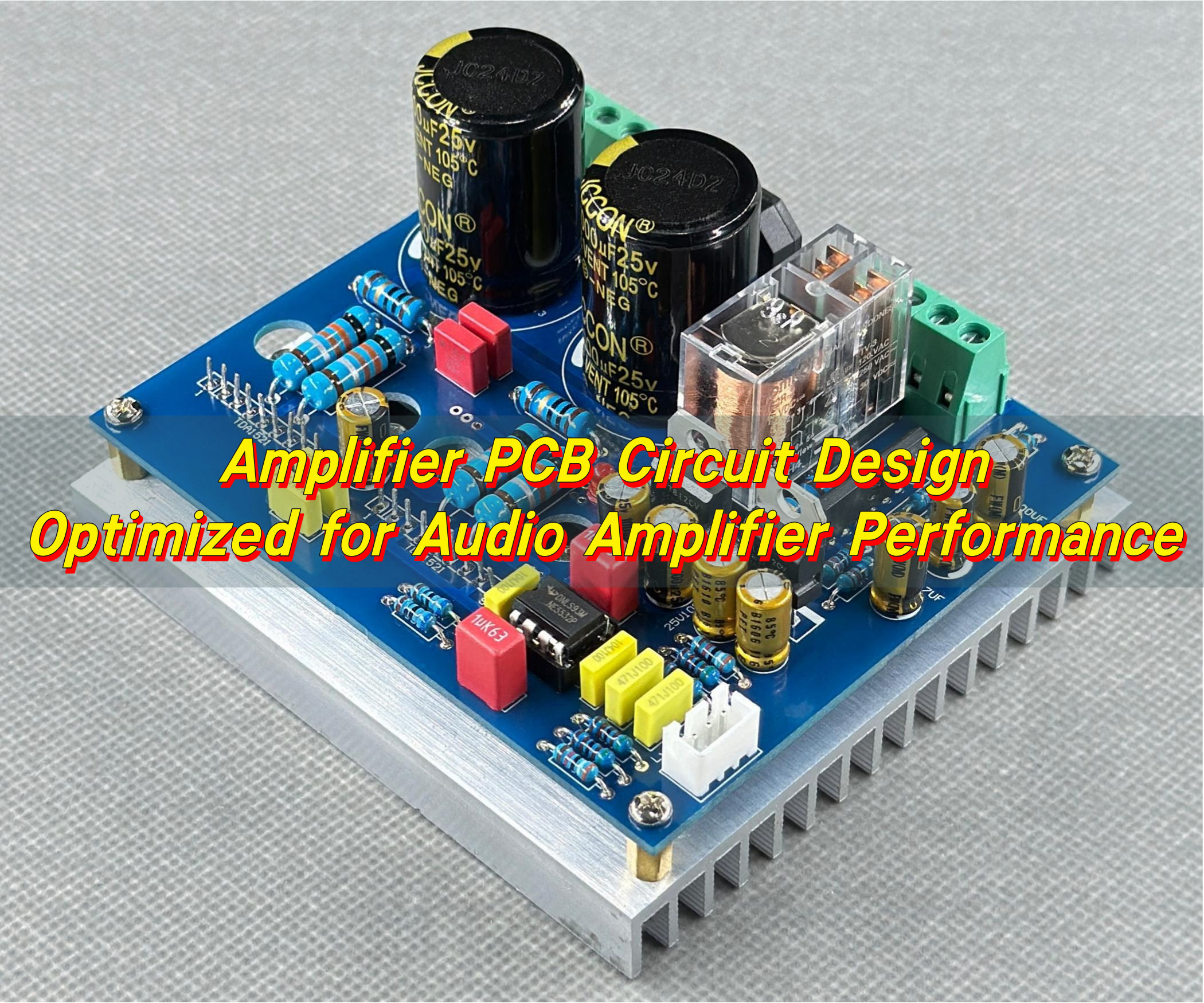
PCB manufacturing PCB manufacturing
Home > Blog

amplifier circuit PCB

What Is an Amplifier Circuit PCB and How to Optimize Layout?
Wednesday, April 15th, 2026

An amplifier circuit PCB​ is a specialized printed circuit board designed to support and interconnect components that increase signal amplitude while maintaining fidelity. This article explores its types, design strategies, high-power builds, component selection, common issues, and selection criteria to help you optimize layout and performance.

Designing reliable amplifier circuits often comes with challenges that can derail projects.

  • Poor signal integrity due to mismatched trace impedance
  • Thermal management failures causing component damage
  • Ground loop noise and EMI interference
  • Difficulty scaling from prototype to mass production
  • High cost and long lead times for custom layouts

To address these pain points, EBest Circuit (Best Technology) offers professional amplifier PCB​ manufacturing and assembly services tailored for optimal performance and manufacturability.

  • Impedance-controlled routing and PCB traces art​ for signal clarity
  • Integrated thermal vias and copper pours for heat dissipation
  • Star grounding and shielding techniques to suppress EMI
  • DFM-optimized layouts ensuring smooth mass production
  • Fast-turn prototyping and volume production with transparent pricing

EBest Circuit (Best Technology) is a leading PCBA manufacturer specializing in high-performance amplifier circuit PCB​ solutions. With advanced fabrication capabilities and strict quality control, we deliver reliable boards for audio, RF, and industrial applications. Pls feel free to contact us at sales@bestpcbs.com for expert support.

amplifier circuit pcb

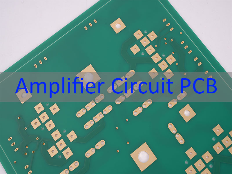
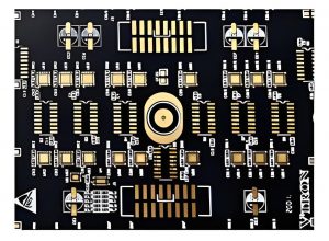
What Is an Amplifier Circuit PCB?

An amplifier circuit PCB​ is the engineered foundation that mechanically supports and electrically connects all components required to increase the amplitude of a signal—whether audio, radio frequency (RF), or power. Beyond simple connectivity, it manages critical factors like power delivery, signal integrity, and heat dissipation to ensure stable, high-fidelity performance.

Depending on the application, different base materials and technologies are selected to meet specific electrical and thermal demands. The most common types used in amplifier PCB​ manufacturing include:

  • FR-4 (Standard): The most widely used substrate for general-purpose amplifier circuit boards, offering a balance of cost, mechanical strength, and electrical insulation. Ideal for consumer audio and mid-power designs.
  • High-Tg FR-4: Modified for higher glass transition temperatures, providing better thermal stability and reliability for power amplifier circuit PCB layout​ in demanding environments.
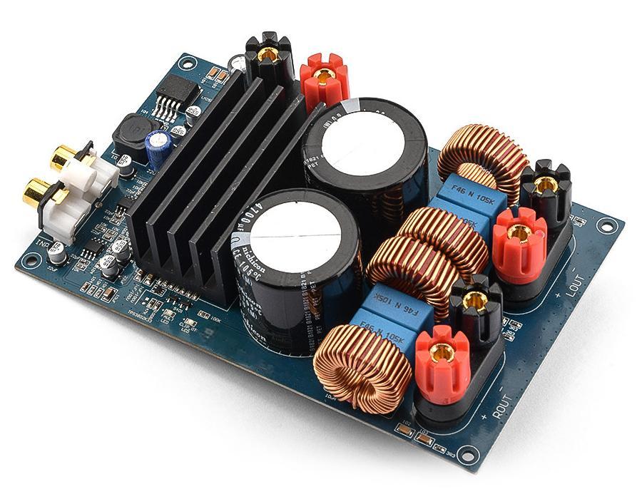
  • HDI (High-Density Interconnect): Utilizes microvias and fine lines to accommodate complex PCB amplifier circuit​ designs with high component density, often used in compact Class D amplifiers.
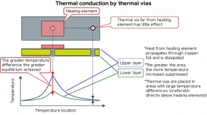
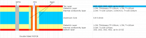
  • Metal Core PCB (MCPCB): Features an aluminum or copper base for superior thermal conductivity, essential for 3kw power amplifier driver circuit PCB layout​ where heat management is critical.
  • RF/Microwave Laminates (e.g., Rogers): Low-loss materials designed for high-frequency applications, crucial for class d amplifier circuit PCB layout​ and wireless communication amplifiers to maintain signal purity.

By selecting the right board type and layout strategy, designers can effectively manage the trade-offs between performance, size, and cost in any amplifier circuit PCB​ project.

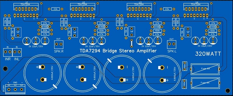
What Are the Key Types of Amplifier PCB Circuits?

Amplifier PCBs vary by application and topology:

TypeTypical UseKey Feature
Audio Amplifier PCBHome/car audioLow distortion, high fidelity
RF Amplifier PCBWireless commsHigh-frequency stability
Class D Amplifier PCBEfficient power ampsPWM switching, compact size
Instrumentation Amp PCBSensors/measurementHigh CMRR, precision
Power Amplifier PCB1000W–3KW systemsRobust thermal handling

How to Design a High-Performance Amplifier PCB Layout?

Optimizing an amplifier circuit PCB layout​ requires attention to signal paths, grounding, and thermal design.

  • Keep input and output traces short and separated to avoid feedback
  • Use ground planes and star grounding to minimize noise
  • Place decoupling capacitors close to power pins
  • Implement thermal vias under high-power devices
  • Follow power amplifier circuit PCB layout​ best practices for EMI reduction

For complex designs like a 1000w amplifier circuit diagram PCB, simulation tools help validate signal integrity before fabrication.

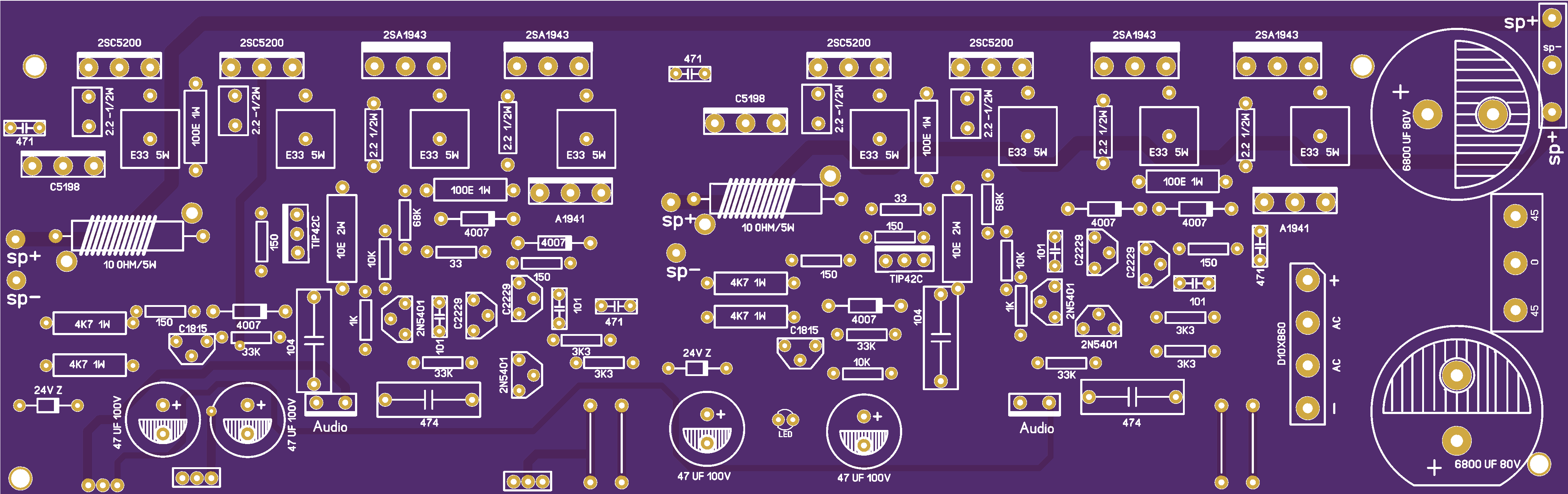
How to Build a 1000W or 3KW Power Amplifier PCB?

High-power builds demand careful planning:

  • Select MOSFETs or IGBTs rated for voltage/current
  • Use thick copper (2oz–4oz) for current-carrying traces
  • Design 3kw power amplifier driver circuit PCB layout​ with adequate heatsinking
  • Ensure proper isolation between high-voltage and low-voltage sections
  • Validate with thermal imaging and load testing

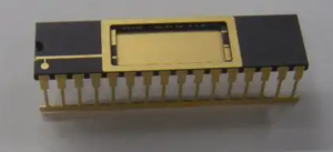
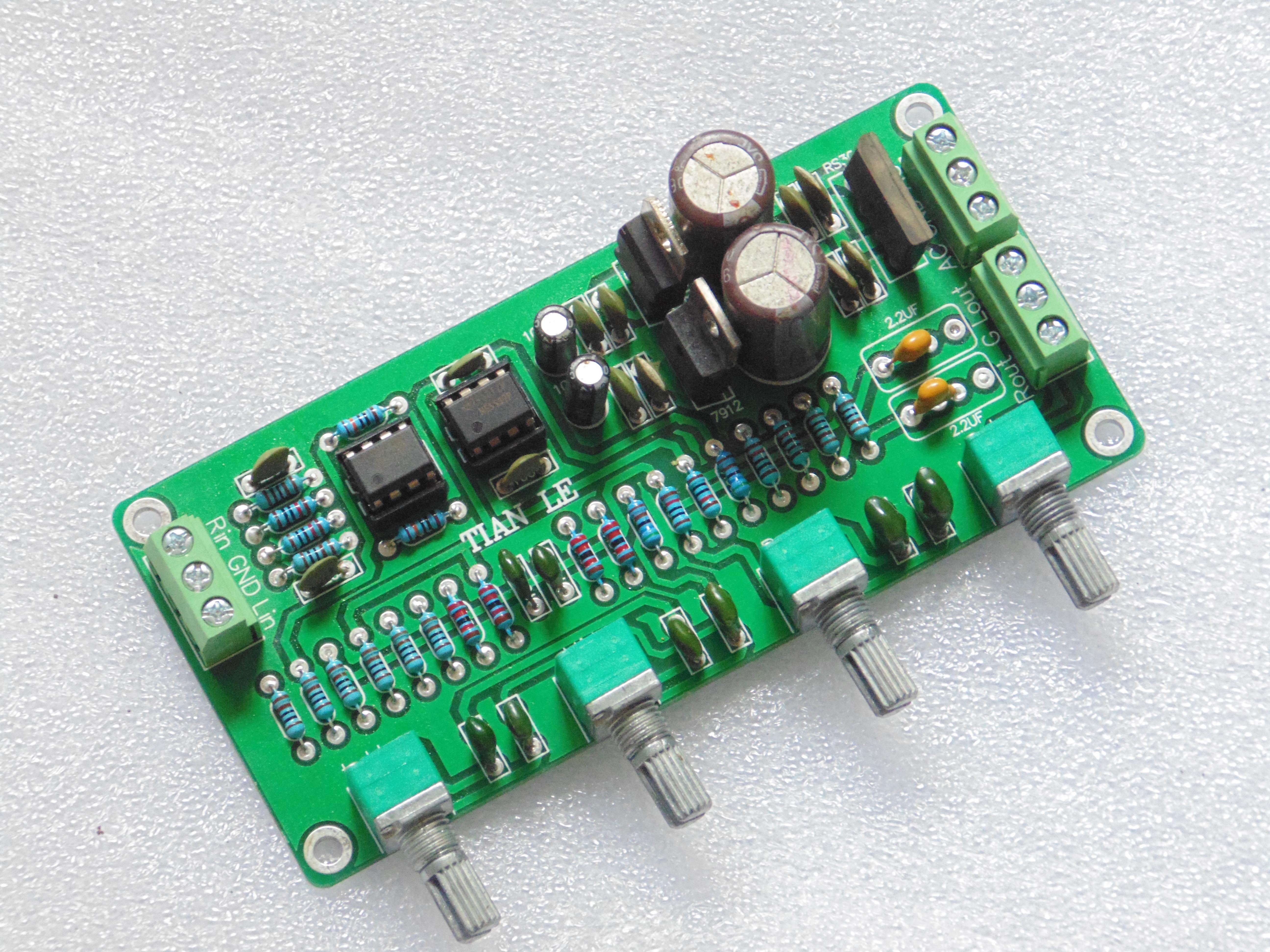
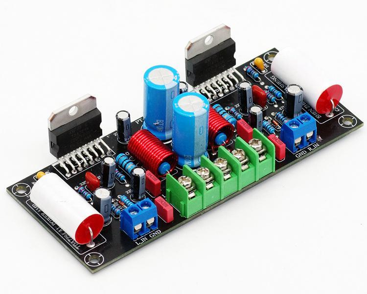
What Components Are Used in an Amplifier Circuit PCB?

Core components include:

  • Amplification devices: BJTs, MOSFETs, op-amps, Class D ICs
  • Passive elements: Resistors, capacitors, inductors for filtering
  • Protection circuits: Fuses, TVS diodes, thermal sensors
  • Connectors: Audio jacks, terminal blocks, RF connectors

A typical PCB amplifier circuit​ integrates these for stable gain and protection.

Common Problems in Amplifier PCB Layout and How to Fix Them

ProblemCauseSolution
OscillationPoor grounding, long feedback loopsShorten traces, improve grounding
OverheatingInadequate copper, no thermal viasAdd vias, increase copper area
Noise/humGround loops, unshielded tracesStar ground, shield sensitive lines
DistortionIncorrect biasing, poor layoutVerify bias points, optimize routing
Failure to startPower sequencing issuesAdd soft-start or delay circuits

How to Choose the Right Amplifier PCB for Your Application?

Consider:

  • Required power output (e.g., 1000W vs 3KW)
  • Frequency range and signal type
  • Environmental conditions (temperature, vibration)
  • Size and form factor constraints
  • Budget and production volume

Matching specs to needs ensures optimal performance from your amplifier circuit board.

Overall, an amplifier circuit PCB​ is essential for delivering clean, amplified signals across audio, RF, and power applications. This guide covered definitions, types, layout optimization, high-power design, components, troubleshooting, and selection criteria to help you build better boards. For expert manufacturing and assembly of amplifier PCB​ solutions, pls feel free to contact us anytime at sales@bestpcbs.com.

FAQs About Amplifier Circuit PCB

Q: Can I use a standard PCB for a power amplifier?

A: Not recommended—high-current designs need thicker copper and thermal management.

Q: What’s the difference between Class AB and Class D layouts?

A: Class D uses switching topology requiring careful EMI control; Class AB is linear but less efficient.

Q: How do I reduce noise in my amplifier PCB?

A: Use proper grounding, shielding, and keep analog/digital sections isolated.

Q: Do you provide power amplifier circuit diagram with PCB layout​ services?

A: Yes, EBest Circuit offers full design-to-production support.

Q: What file formats do you accept?

A: Gerber, ODB++, and Altium files are preferred.

Amplifier PCB Circuit | High-Fidelity Low-Noise Audio PCB Design
Tuesday, February 3rd, 2026

Need professional amplifier PCB circuit design? We provide optimized PCB circuit solutions with precise wiring and impedance matching for high-performance audio amplifiers. Get custom quote here.

Amplifier PCB Circuit | High-Fidelity Low-Noise Audio PCB Design

What Is a PCB in an Amplifier?

PCB in an amplifier is the physical platform that connects and supports all electronic parts required to boost an audio signal. It holds active devices such as transistors or ICs, passive parts like resistors and capacitors, and power components that deliver current to the load.

In an audio amplifier, the PCB does far more than provide mechanical support. It controls impedance, limits interference, and manages heat. From a functional view, an amplifier PCB usually integrates several blocks. These blocks work together on the same board.

Input traces handle tiny signals and need isolation. Output paths carry high current and need wide copper and short routes. The PCB ties these together in a controlled and repeatable way.

What Are the Different Types of Amplifier PCBs?

Amplifier PCBs vary based on function, power level, and application environment. There is no single universal board style. One common way to classify amplifier PCB circuits is by amplifier class.

  • Class A amplifier PCBs favor simplicity and linearity. They generate constant heat and require strong thermal paths.
  • Class AB amplifier PCBs balance efficiency and sound quality. They need careful bias routing and stable grounding.
  • Class D amplifier PCBs switch at high frequency. They demand controlled impedance, tight loop areas, and EMI control.

Another way to group amplifier PCBs is by construction style.

  • Single-layer PCBs appear in low-cost or simple amplifier modules. They are easy to make but limited in performance.
  • Double-layer PCBs are common in consumer audio. They allow better grounding and signal routing.
  • Multilayer PCBs support high-end or compact amplifiers. Dedicated ground and power planes improve noise control.
  • Metal-core PCBs help in power amplifiers where heat dissipation is critical.
  • Rigid-flex PCBs appear in space-constrained or portable audio devices.

Application also influences PCB type. A headphone amplifier PCB looks very different from a 1000-watt PA amplifier PCB. Automotive and industrial amplifiers may need thicker copper, higher Tg materials, or special surface finishes to handle stress.

At EBest Circuit (Best Technology), amplifier PCB projects often range from compact low-noise audio boards to heavy-copper power amplifier PCBs. The board type is selected after reviewing power level, thermal load, and target market.

How Are Amplifier PCB Circuit Design?

  • The first step is schematic planning. Once the schematic is stable, PCB design translates theory into copper.
  • Signal integrity is always a priority. Low-level input signals must be protected from noise sources. These traces should be short, direct, and shielded by ground when possible.
  • Thermal design is another core concern. Output devices and regulators generate heat. The PCB must spread this heat through copper pours, thermal vias, or metal substrates.
  • Power distribution must be stable. Decoupling capacitors should sit close to active devices. Bulk capacitors need short return paths.

Key layout practices include:

  • Keeping high-current loops small
  • Separating signal and power sections
  • Using wide copper for output stages
  • Placing feedback paths carefully
  • Controlling trace impedance in Class D designs

Amplifier PCB circuit design is not only about rules. It also involves experience. Manufacturers like EBest Circuit (Best Technology) often support customers with design feedback, pointing out layout risks before production. That early review saves time and cost later.

Amplifier PCB Circuit | High-Fidelity Low-Noise Audio PCB Design

The Manufacturing Process of a Custom Amplifier PCB Circuit

Once an amplifier PCB circuit design is finalized, manufacturing turns digital files into a physical board. Most audio amplifier PCBs use FR-4, but high-power or high-temperature designs may need high-Tg laminates or metal-core substrates. Copper thickness is chosen based on current load.

The typical manufacturing flow includes several stages.

  • Data preparation, where Gerber files and drill data are checked
  • Inner layer imaging, for multilayer boards
  • Lamination, bonding layers under heat and pressure
  • Drilling, creating vias and mounting holes
  • Plating, adding copper to holes and surfaces
  • Outer layer imaging and etching, forming final traces
  • Solder mask application, protecting copper and defining pads
  • Surface finish, such as ENIG or HASL
  • Electrical testing, verifying connectivity

For amplifier PCBs, quality control is critical. Trace width tolerance affects impedance and current capacity. Via quality affects thermal transfer. Solder mask accuracy affects assembly yield.

Custom amplifier PCB circuits often need tighter inspection than standard digital boards. Audio customers expect low noise and long service life.

EBest Circuit (Best Technology) integrates PCB fabrication with PCBA services, allowing amplifier boards to move smoothly from bare board to assembled unit. That integration reduces handling risk and shortens delivery cycles.

What Are the Advantages of Amplifier PCBs?

Amplifier PCBs offer clear benefits compared to loose wiring or ad-hoc construction.

  • One major benefit is electrical stability. A PCB enforces consistent trace lengths and grounding paths.
  • Another advantage is compact size. PCBs allow dense placement of parts without sacrificing performance.
  • Reliability also improves with PCBs. Fixed copper traces do not loosen like wires.

Key advantages include:

  • Lower noise through controlled grounding
  • Better heat management with copper pours
  • Higher assembly efficiency
  • Easier troubleshooting and repair
  • Scalable production from prototype to volume

Amplifier PCBs also support modern compliance needs. They allow traceability, automated inspection, and standardized testing.

How Does an Amplifier PCB Circuit Work in Audio Amplifier Systems?

An amplifier PCB circuit works by guiding an audio signal through a controlled amplification path while supplying power and maintaining stability. The PCB does not amplify by itself, but it enables each component to do its job correctly.

  • The process begins at the input. The PCB routes the incoming signal to the first gain stage. This area must stay quiet.
  • Next comes voltage amplification. Transistors or ICs increase signal amplitude. The PCB ensures that feedback paths remain stable and short.
  • The output stage then delivers current to the load. This part of the PCB handles high current and heat. Wide traces, thick copper, and solid ground returns are common.
  • Throughout the circuit, the power supply section feeds clean voltage. Decoupling capacitors smooth fluctuations. The PCB keeps these loops tight to prevent ripple and noise from leaking into the signal path.
  • Protection circuits often sit near the output. They monitor temperature, current, or DC offset. The PCB must connect these accurately to respond fast in fault conditions.

In a complete audio amplifier system, the PCB acts as the nervous system. It coordinates signal flow, power delivery, and protection.

Amplifier PCB Circuit | High-Fidelity Low-Noise Audio PCB Design

What Are the Applications of Amplifier PCBs?

Amplifier PCBs appear in many products, far beyond traditional home audio. Any system that needs to boost a signal relies on some form of amplifier circuit PCB.

Common application areas include:

  • Home audio amplifiers and receivers
  • Professional sound systems and mixers
  • Automotive audio and infotainment
  • Headphone amplifiers and DACs
  • Musical instrument amplifiers
  • Public address systems
  • Industrial signal amplification
  • Medical and measurement equipment

Each application places different demands on the amplifier PCB circuit. Home audio focuses on low noise and clean sound. Automotive amplifiers need vibration resistance and temperature tolerance. Industrial systems demand long-term stability.

EBest Circuit (Best Technology) works with customers across these sectors, supporting both low-volume prototypes and stable mass production.

How to Choose a Custom Amplifier PCB Circuit Supplier?

Choosing the right supplier for an amplifier PCB circuit is a strategic decision. The supplier influences performance, cost, delivery, and long-term reliability.

  • Technical capability should come first. The supplier must understand audio-specific challenges such as noise control, thermal design, and high-current routing.
  • Manufacturing range also matters. A good supplier supports different board types, copper weights, and finishes.
  • Quality systems are another key factor. Certifications, inspection methods, and traceability protect your product reputation.
  • Communication style matters more than many expect. Amplifier PCB projects often evolve during prototyping.

When evaluating suppliers, consider these points:

  • Experience with amplifier PCB circuits
  • Support for DFM and layout review
  • Stable material sourcing
  • Clear quality control process
  • Ability to scale from prototype to volume

EBest Circuit (Best Technology) positions itself as a one-stop PCB and PCBA partner. By combining fabrication and assembly, it helps audio amplifier projects move faster with fewer handoffs.

Amplifier PCB Circuit | High-Fidelity Low-Noise Audio PCB Design

Conclusion:

An amplifier PCB circuit is the foundation of audio amplifier performance. It shapes signal integrity, controls noise, manages heat, and ensures consistency from unit to unit. From basic input routing to high-current output stages, every layout decision affects sound quality and reliability.

If you are developing a custom amplifier PCB circuit and want a partner who understands audio requirements, manufacturing precision, and scalable production, EBest Circuit (Best Technology) can support your project from concept to delivery.

For technical consultation or a quotation, please contact sales@bestpcbs.com