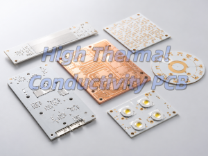
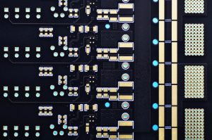
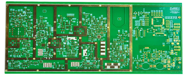
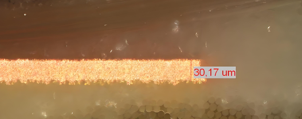
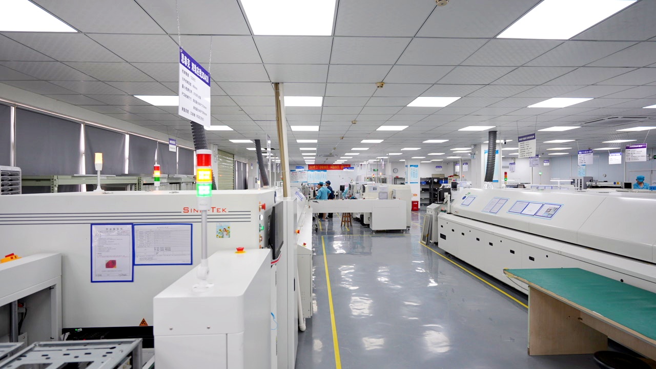
An aluminium substrate PCB is a metal core PCB that uses aluminum as its base layer instead of fiberglass. This design improves heat dissipation, strengthens the board, and enhances reliability.
It’s widely used in high-power applications like LED lighting and power supplies because it keeps components cooler and extends their lifespan. With excellent thermal performance and solid durability, aluminum PCBs are a smart choice for demanding electronic designs.
What is aluminum substrate?
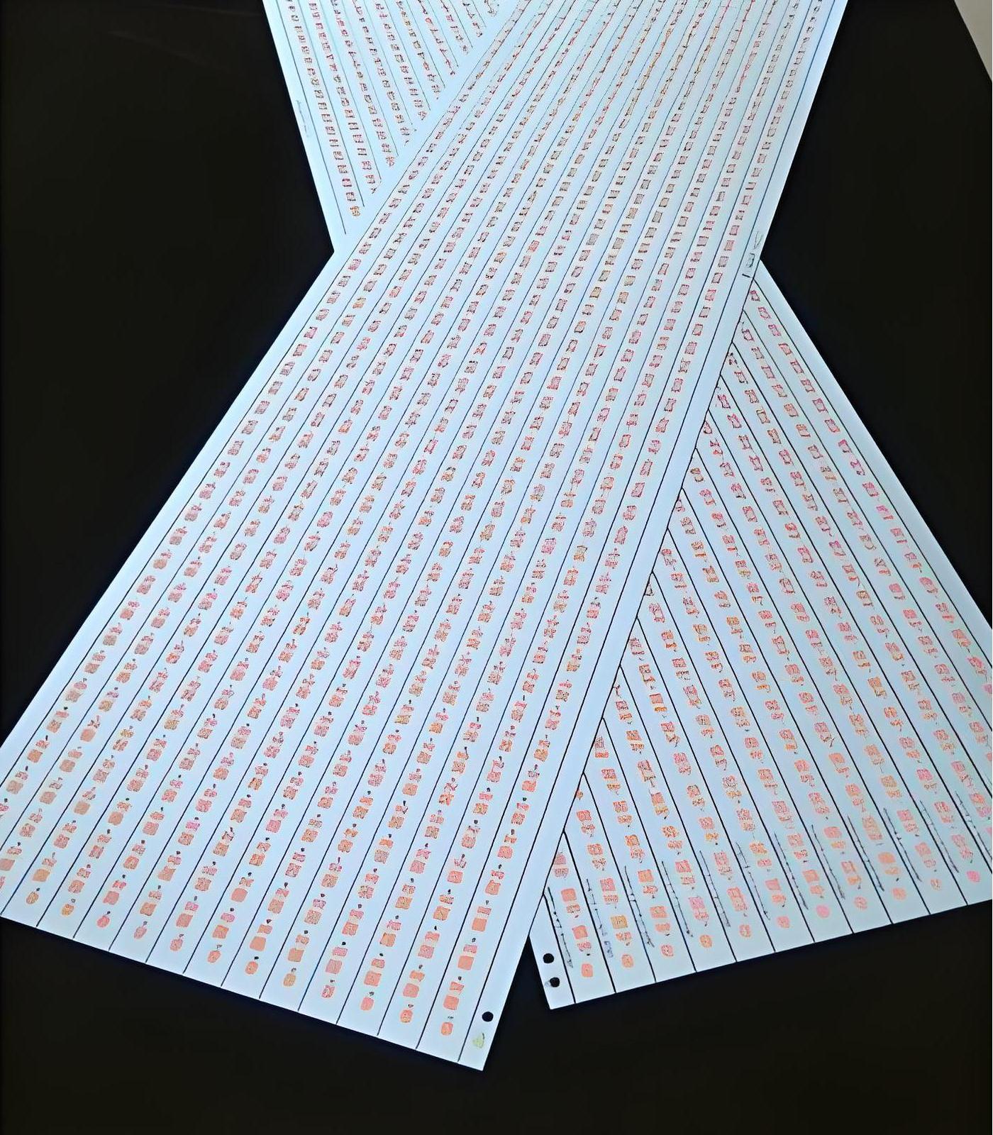
The aluminium substrate in a PCB refers to the base layer made from aluminium instead of standard fiberglass. In a typical PCB, this layer would be FR4 or other resin materials. But with aluminium substrate PCBs, the core material is metal—specifically aluminium.
This aluminium base gives the PCB a solid foundation. It’s known for exceptional thermal conductivity and mechanical strength. When electronics generate heat (which they always do), this base layer helps pull the heat away fast. That means better performance, less risk of damage, and a longer product lifespan.
Aluminium also gives the board added durability. In harsh environments, it resists physical stress and corrosion better than many other substrates.
What is substrate in PCB?
To put it simply, a substrate in a PCB is the backbone. It’s the main layer that supports everything else. Think of it as the canvas where all the components and copper traces are placed.
The choice of substrate affects how a PCB behaves—its strength, heat resistance, flexibility, and even cost. Most traditional PCBs use FR4, a fiberglass-reinforced epoxy laminate. But when you need better thermal performance, a metal core like aluminium becomes the better option.
The aluminium substrate works by absorbing and dispersing heat, unlike FR4, which traps it. This becomes crucial in power devices, LEDs, and RF systems.
What is the difference between aluminum and FR4 PCB?
The contrast between aluminium and FR4 PCBs is more than just materials—it’s about function, reliability, and endurance.
- Material: Aluminium PCBs have a metal core. FR4 PCBs use a glass epoxy material.
- Thermal Conductivity: Aluminium wins. It conducts heat away quickly. FR4 holds onto heat, which can cause issues in high-power circuits.
- Durability: Aluminium is tougher. It resists wear, shock, and even moisture better.
- Weight: FR4 is lighter and more flexible, which is good for some consumer electronics.
- Cost: Aluminium PCBs tend to be more expensive to produce but save money by increasing product lifespan and reliability.
So, while both have their place, aluminium PCBs provide real advantages in power-driven or heat-sensitive applications.
Why is aluminum no longer used in integrated circuits?
There was a time when aluminium was the go-to material for IC interconnections. It worked well in early semiconductor technologies. But as chips became smaller and faster, aluminium began to show limits.
Why? Copper is more conductive than aluminium. That means it handles signals faster and uses less power. It also allows for smaller, more compact designs.
Aluminium hasn’t disappeared, though. It’s just moved to a different job—serving as the base in PCBs where strength and heat transfer matter most.
Can high frequency PCB replace aluminium PCB?
High-frequency PCBs are designed to handle fast signals with minimal loss. They use specialized materials like PTFE (Teflon) to maintain signal integrity. But they don’t handle heat as well as aluminium PCBs.
So, can one replace the other? Not really. They serve different purposes. High-frequency PCBs are great for communication systems, radar, and RF devices. Aluminium PCBs are perfect when heat is a big issue—like in power supplies or LED systems.
That said, some advanced designs do combine both features. But in most cases, high-frequency and aluminium PCBs are used in their own unique ways.
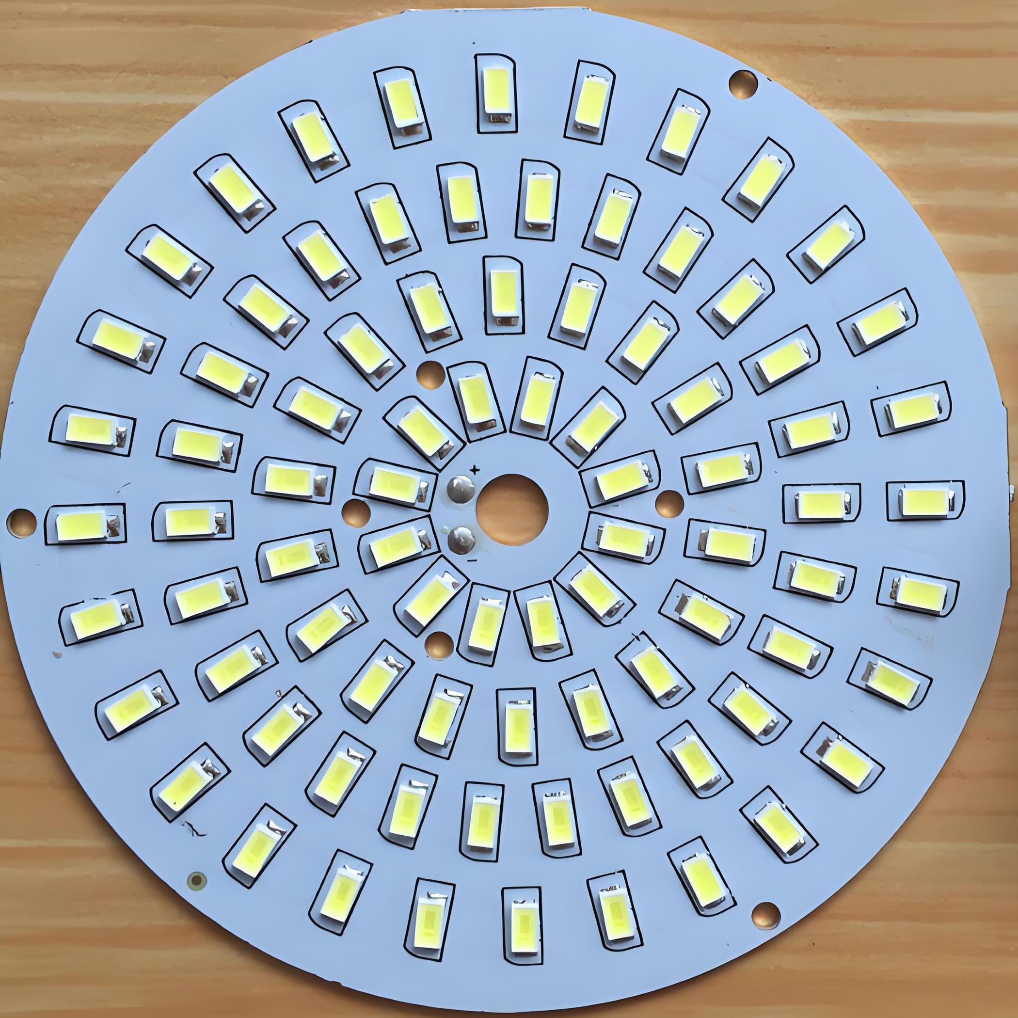
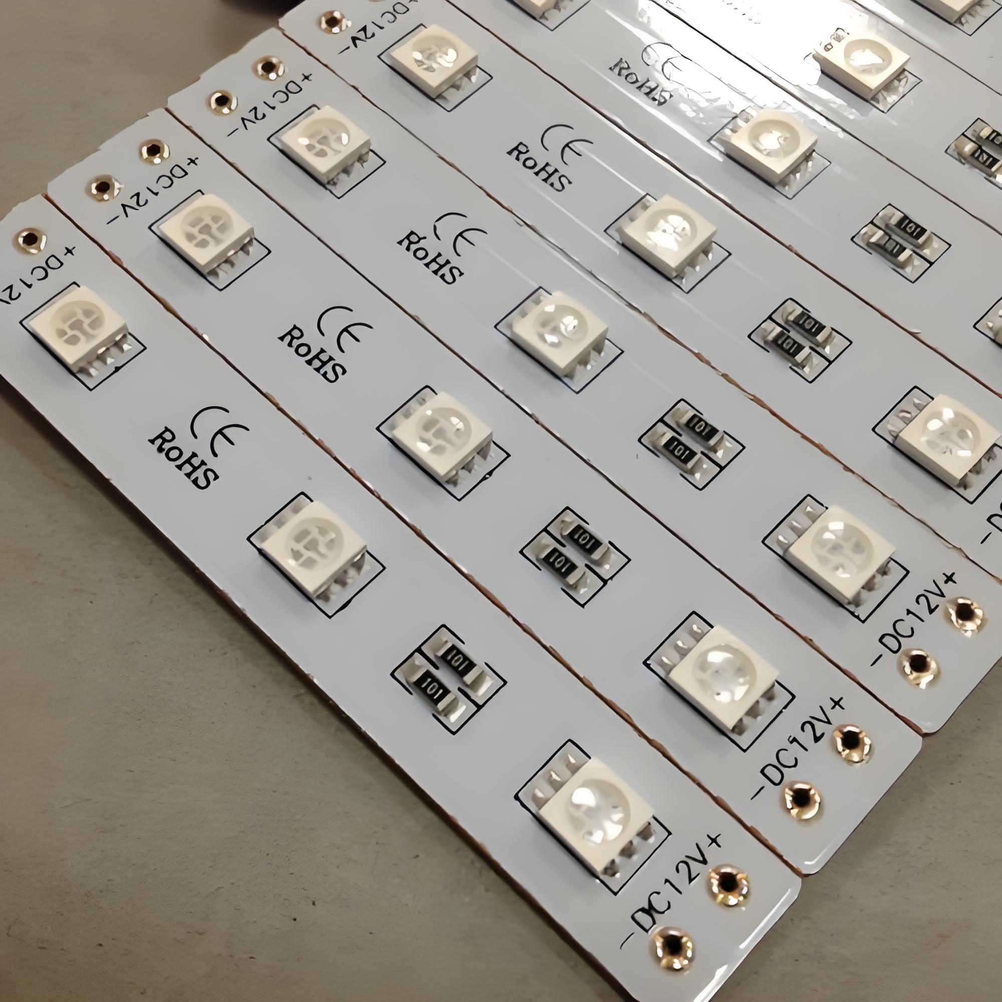
Why use aluminium-substrate-PCB for LEDs?
LEDs are efficient light sources, but they generate concentrated heat. If not properly managed, that heat shortens lifespan, dims brightness, and even causes failure. That’s why aluminium-substrate-PCBs are a top choice for LED systems.
Also, aluminium PCBs provide a stable platform. They resist bending or cracking, even in high-humidity or high-temperature environments.
When used in LED strips, light panels, or automotive lights, aluminium PCBs ensure consistent brightness, lower energy loss, and better reliability.
Energy savings also come into play. With better heat dissipation, less power is wasted as heat. That means more energy is turned into light.
What are the pros and cons of aluminum PCB?
Like every technology, aluminium PCBs come with benefits and some limitations. Let’s look at both sides.
Pros:
- Superior Heat Dissipation: This is the biggest win. Aluminium handles heat far better than FR4.
- High Strength: Aluminium resists cracking, breaking, and vibration. That makes it ideal for industrial and automotive applications.
- Longevity: Better cooling leads to longer component life. That reduces maintenance and repair costs.
- Eco-Friendly: Aluminium is recyclable. That makes it a green choice for modern electronics.
- Thermal Stability: It maintains performance even when temperatures rise.
Cons (but minimal):
- Higher Cost: Aluminium PCBs cost more to produce than FR4.
- Less Flexibility: Aluminium is rigid. It’s not suitable for bendable or foldable circuit designs.
- Machining Complexity: Cutting and drilling aluminium is harder than standard boards.
If your application needs thermal stability, strength, and reliability, the pros easily outweigh the cons.
What are aluminum PCBs used for?
The reach of aluminium PCBs is wide. Their applications span multiple industries and product types.
- LED Lighting: From household bulbs to industrial fixtures, aluminium PCBs keep LEDs cool and long-lasting.
- Automotive Electronics: Think dashboard lighting, engine control systems, and electric vehicle modules.
- Power Supplies: High-wattage power converters, inverters, and regulators benefit from aluminium’s heat handling.
- Telecom Equipment: Signal amplifiers and antenna systems use aluminium PCBs for thermal control.
- Medical Devices: Precision tools like scanners and monitors require stability and heat protection.
- Consumer Products: High-performance gadgets like gaming devices, laptops, and audio systems often use metal core boards to ensure smooth operation.
No matter the product, if heat or durability is a concern, aluminium-substrate-PCB is often the right solution.
Conclusion:
Aluminium substrate PCBs are more than just metal-backed boards. They are performance boosters. They protect your devices from heat, shock, and failure. From LED lighting to telecom and automotive systems, these boards make sure devices run cooler, longer, and more efficiently.
If you’re designing products that need to handle heat, perform reliably, and last longer—aluminium PCBs are a smart, solid investment.
Need help choosing or customizing your aluminium-substrate-PCB? Contact us now at sales@bestpcbs.com