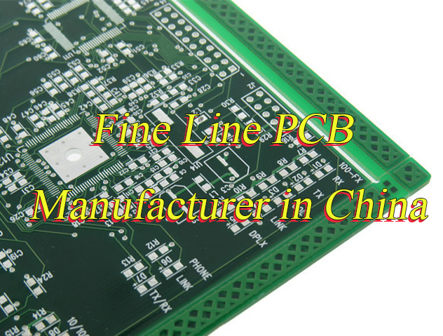
Why use barebones PCB? Let’s discover its benefits, application, design spec and guide, production process, cost for barebones PCB together.
Are you worried about these questions?
- Does trace width/spacing design often hit process limits, causing costly reworks?
- Struggling with high NRE costs and material waste for small-batch/rush orders?
- Suffering signal integrity issues from improper substrate selection or impedance mismatch?
As a barebones PCB manufacturer, EBest Circuit (Best Technology) can provide you services and solutions:
- Free DFM Pre-Scan: Auto-checks 18+ parameters (trace/spacing, via match) to flag risks pre-production, cutting prototyping costs.
- Smart Panelization & Material Matching: Optimizes panel layout by order volume, compares FR-4/high-speed substrates in real-time, reducing small-batch costs by 15-20%.
- Flexible Delivery: Standard 5-7 days or 1-3 days express with transparent tracking, backed by 20 years of process expertise for reliable quality, not just speed.
Welcome to contact us if you have any request for barebones PCB: sales@bestpcbs.com.
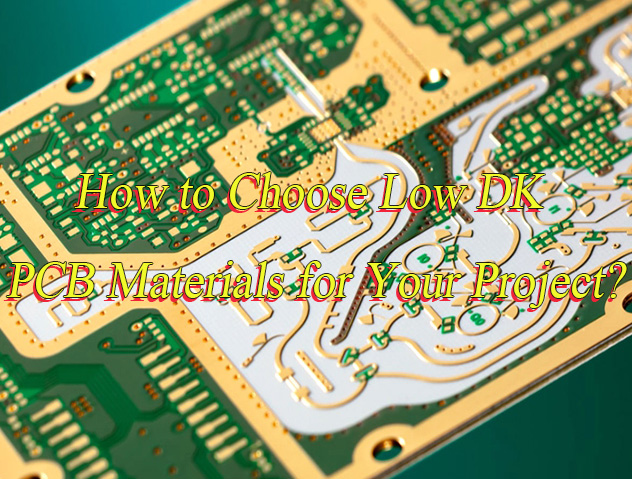
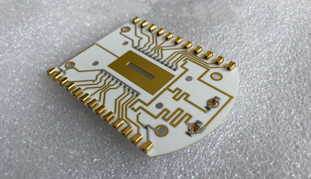
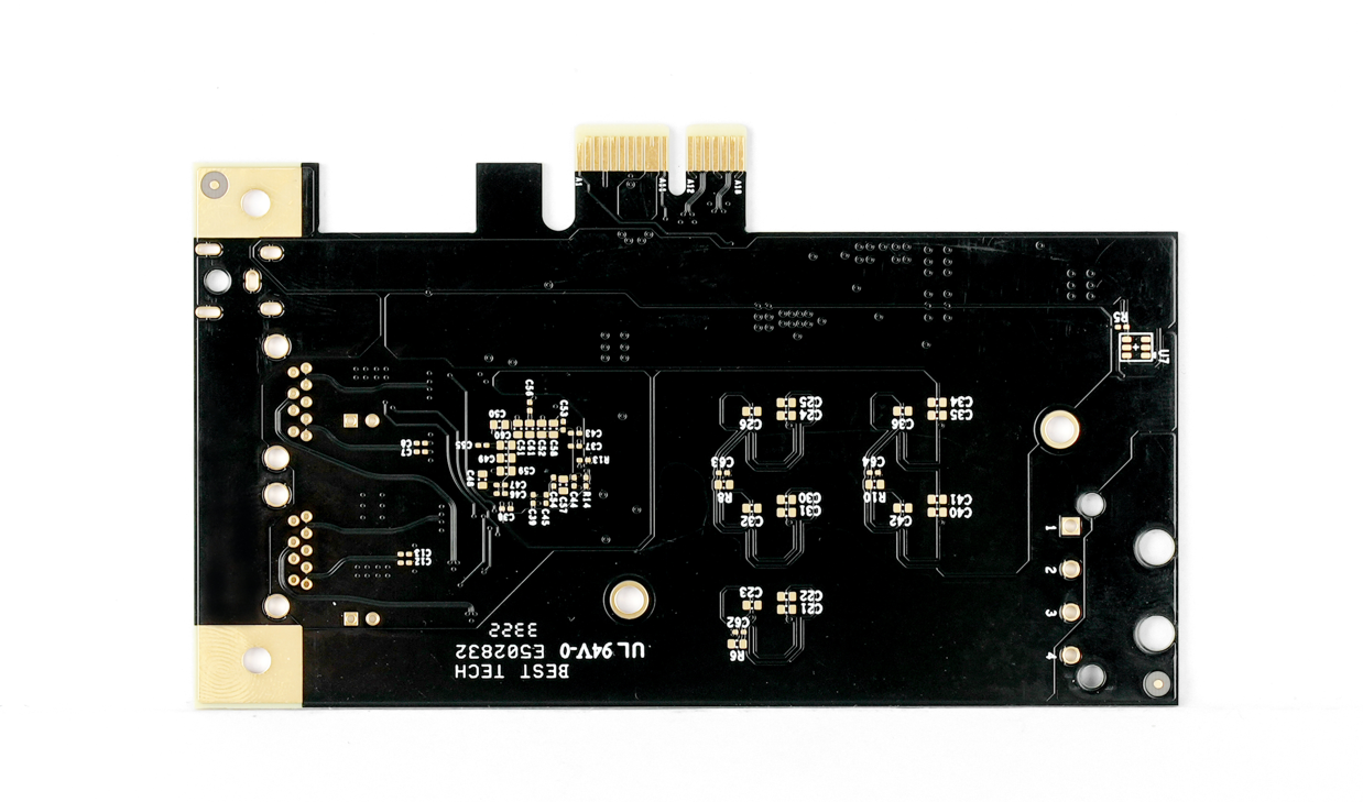
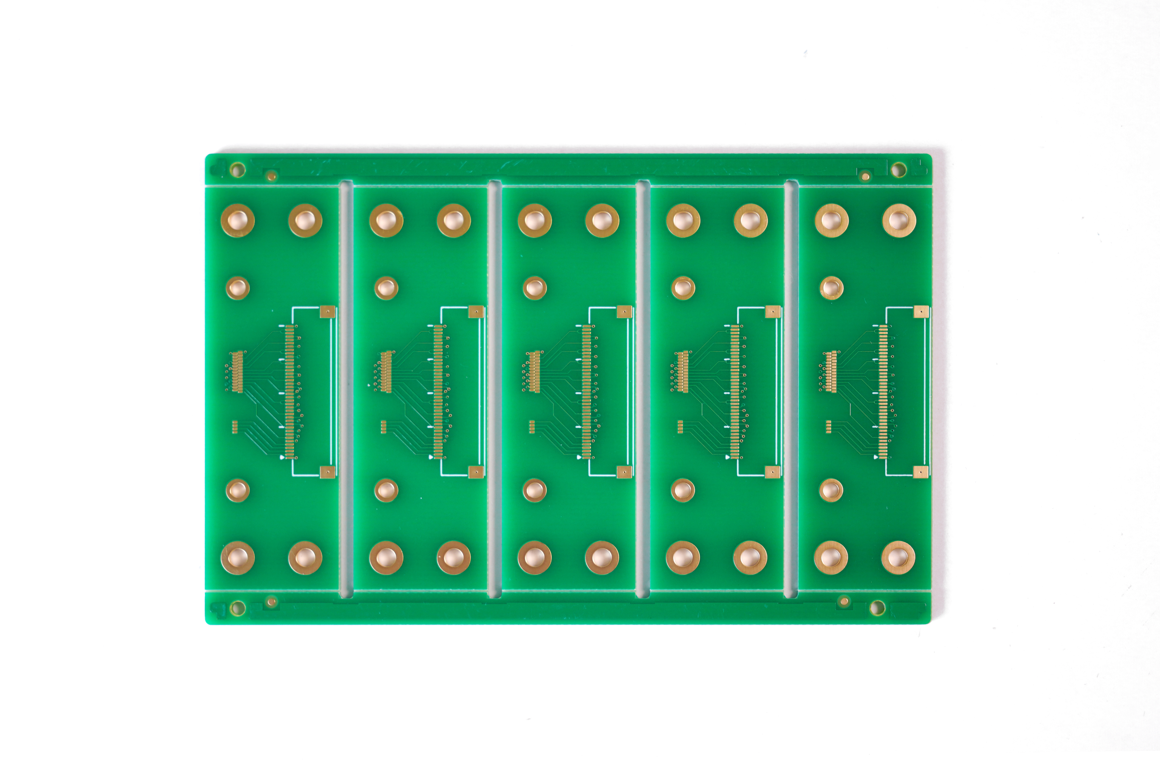
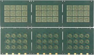
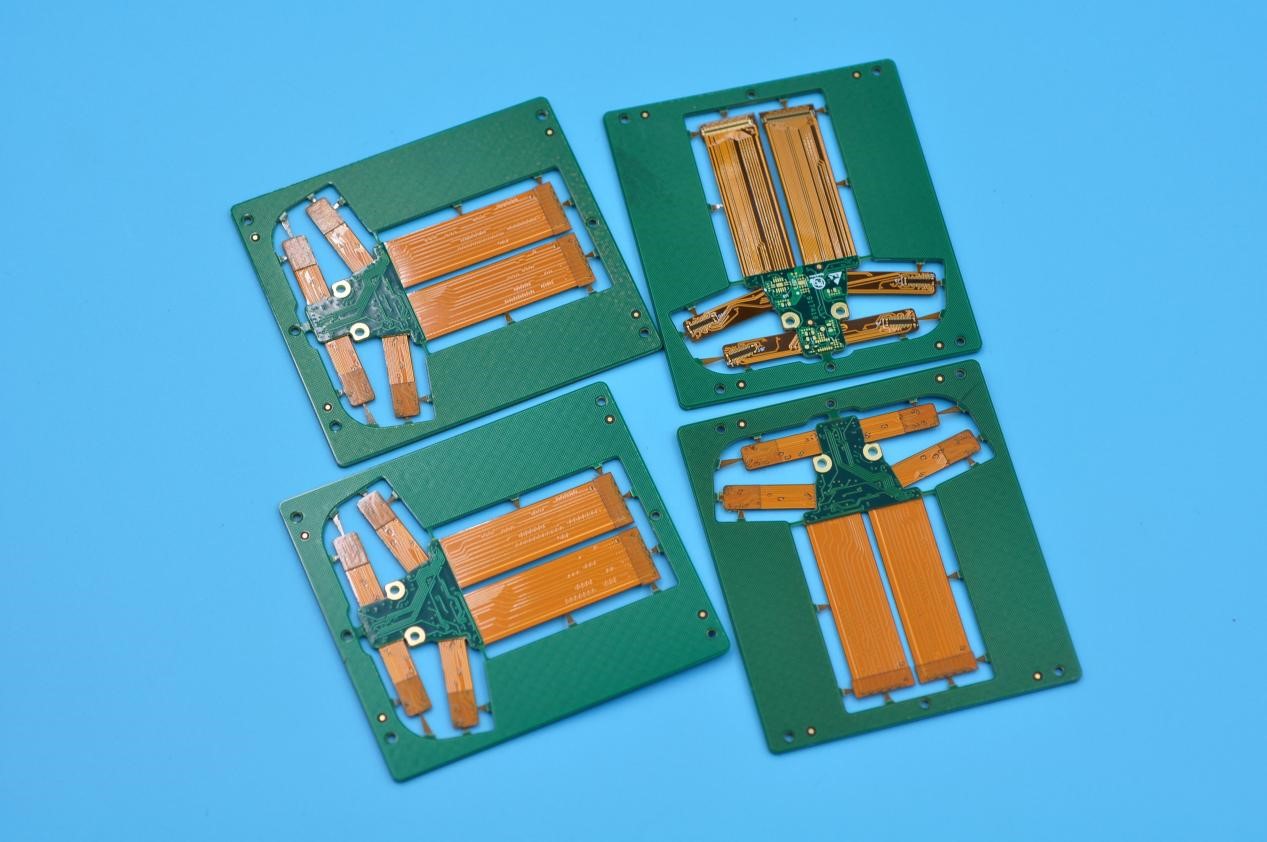
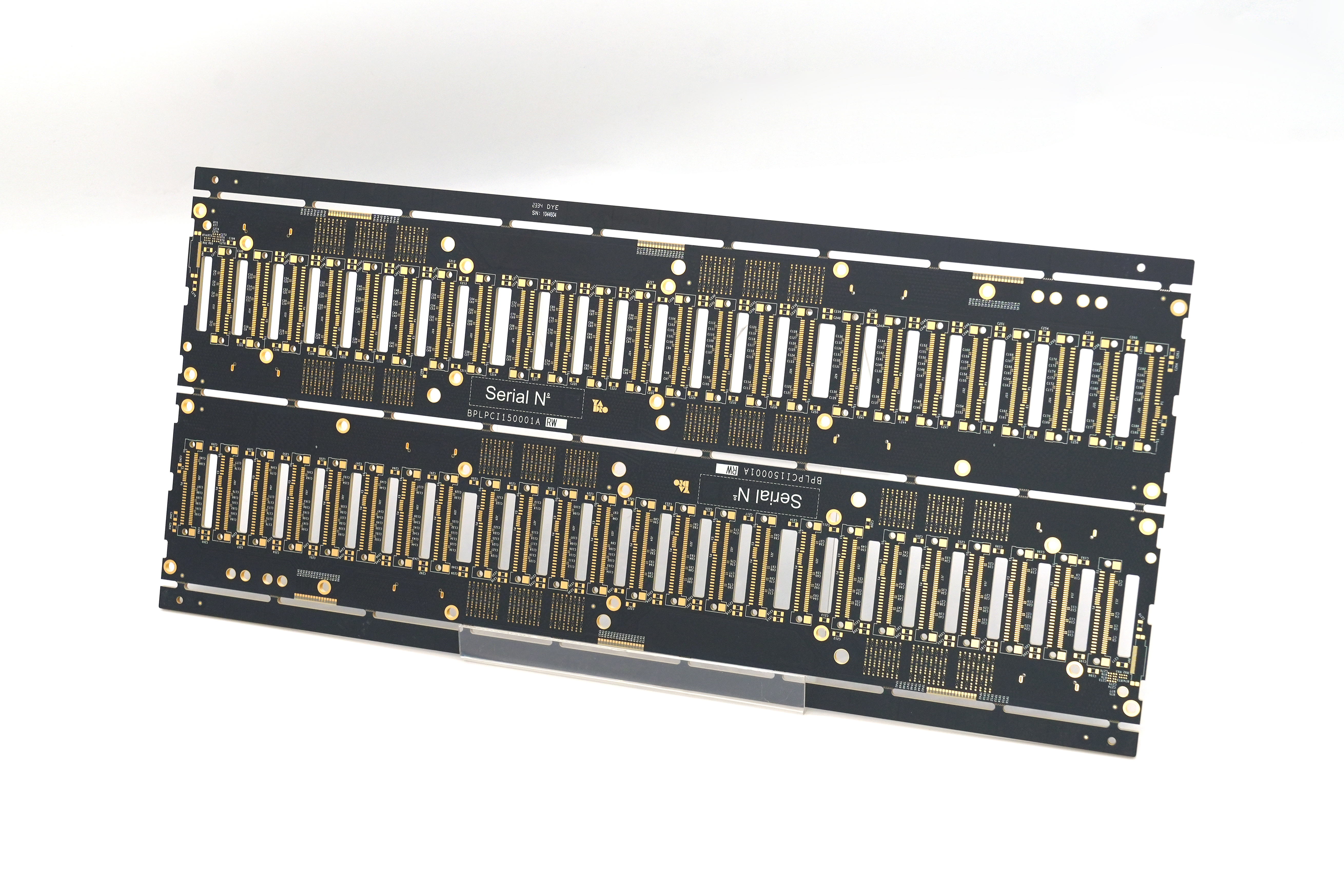
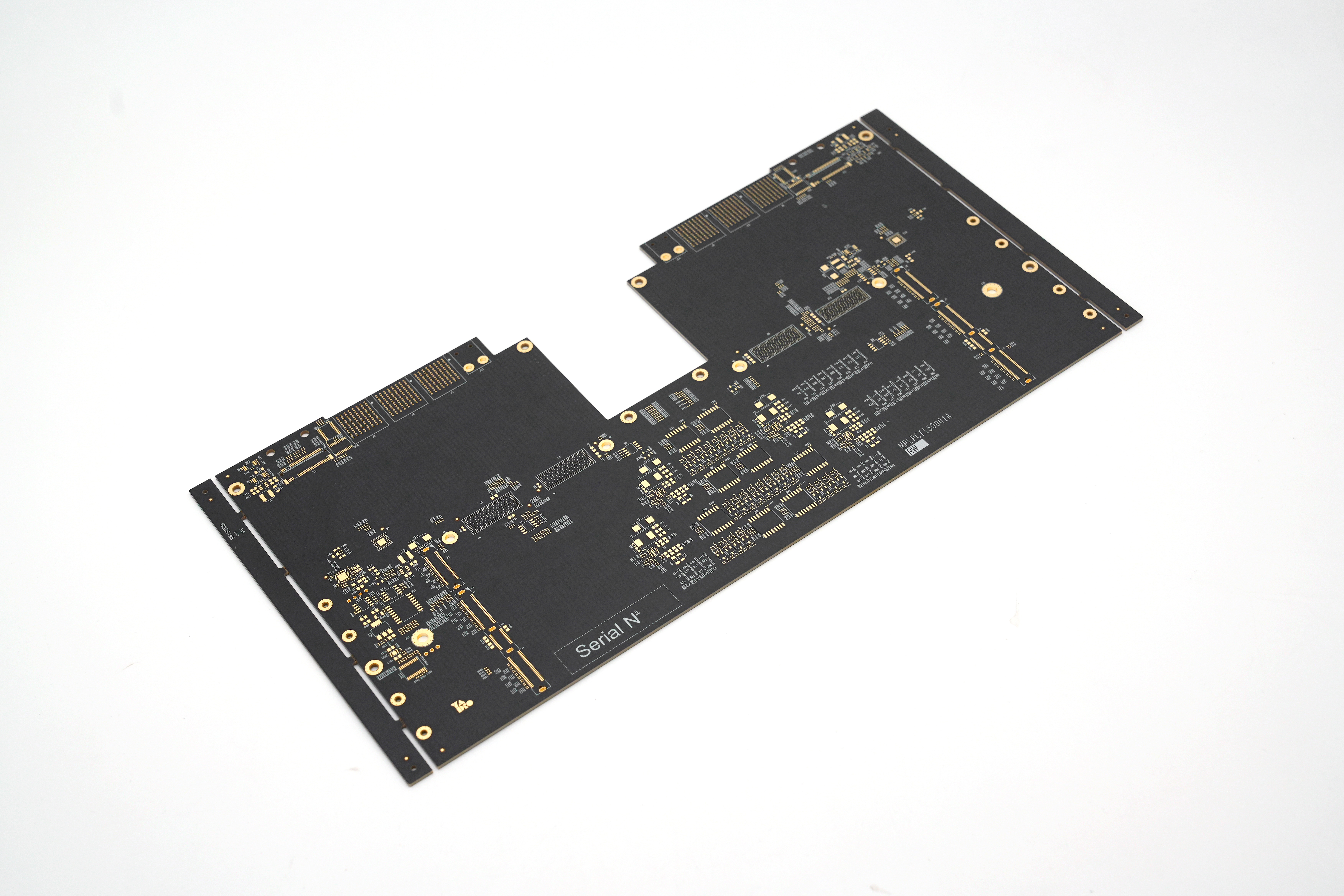
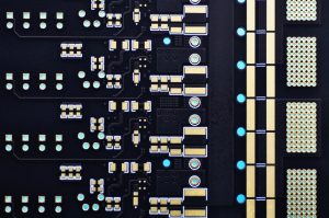
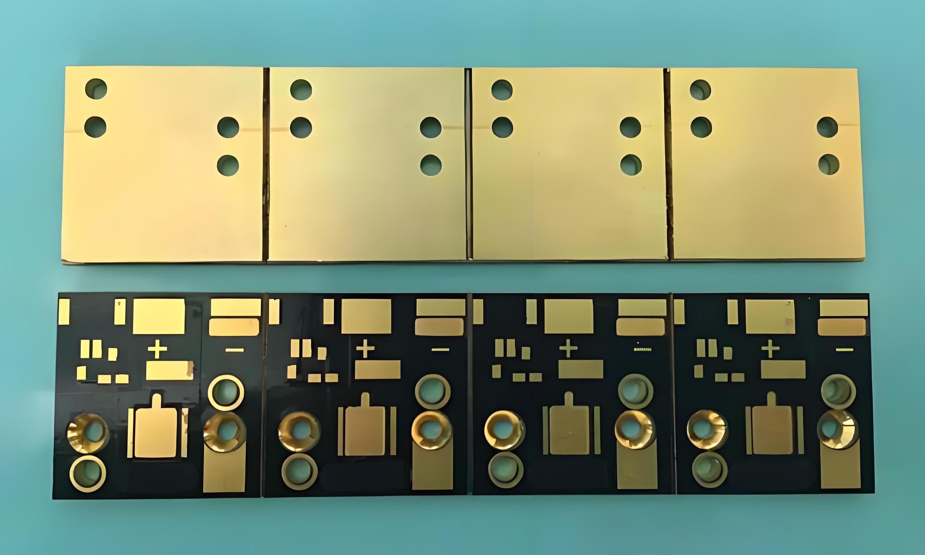
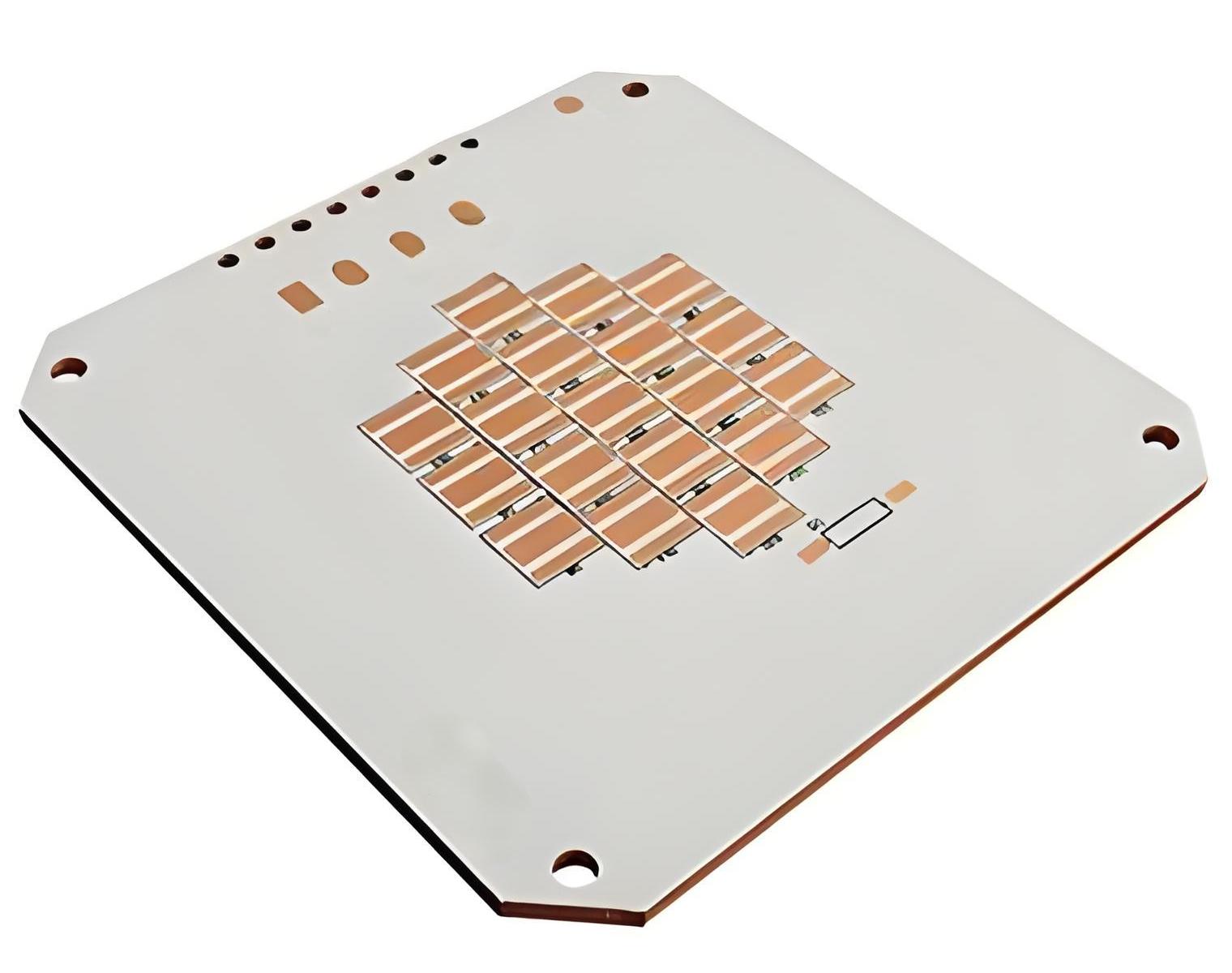
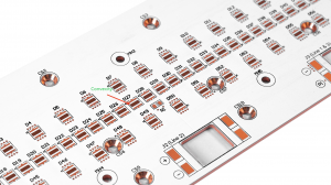
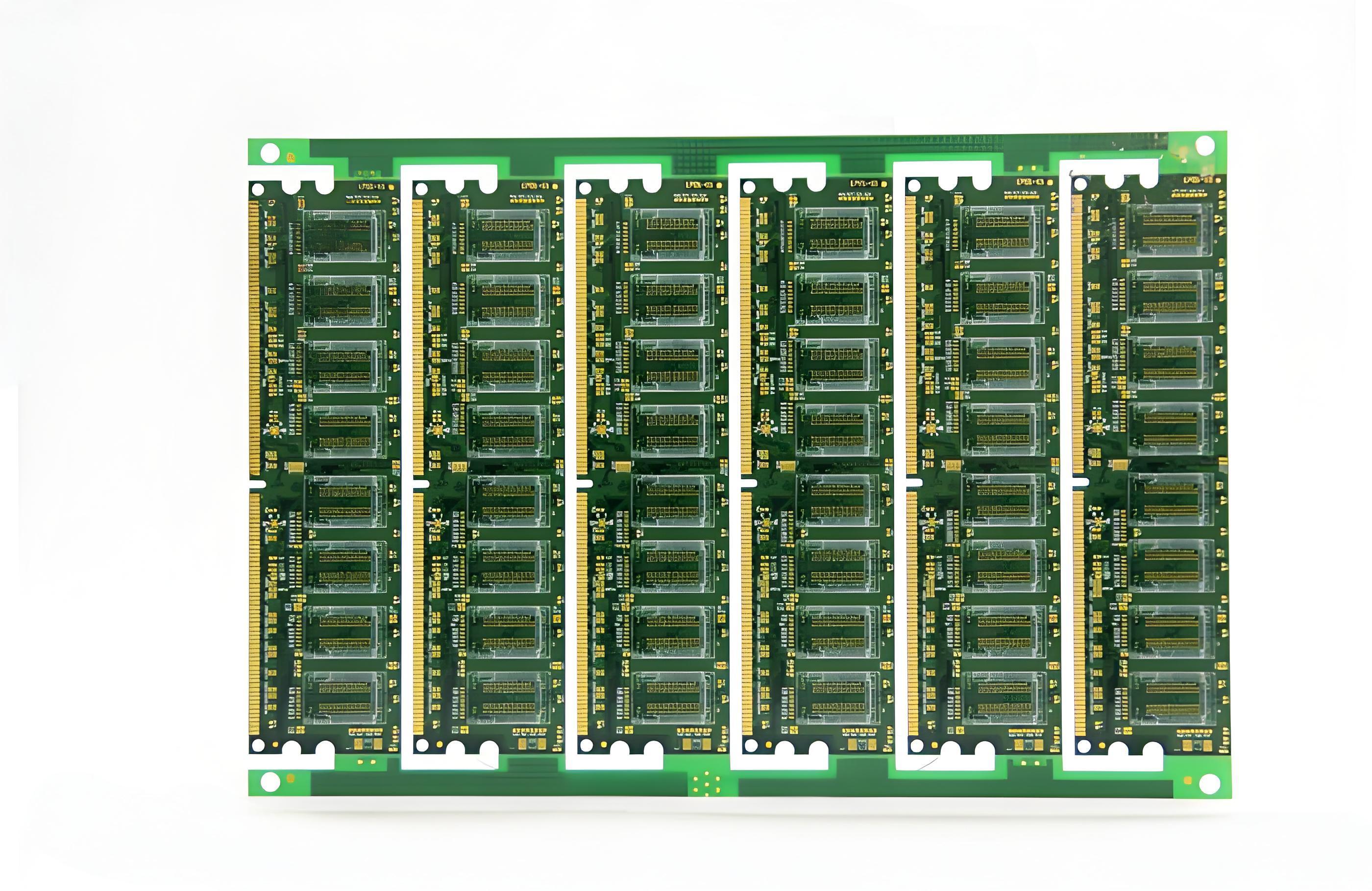
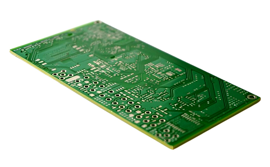
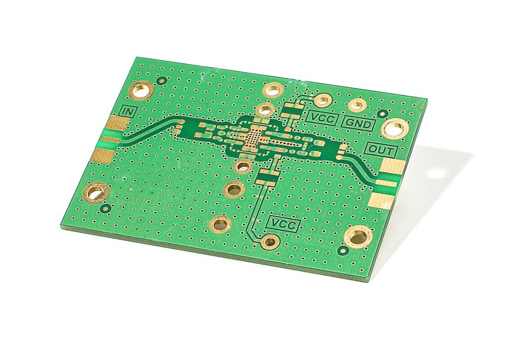
What Is a Barebones PCB?
A Barebones PCB (foundational printed circuit board) is a minimalist circuit board that retains only core conductive traces and pads while omitting non-essential structures such as solder mask, silkscreen layers, or complex multi-layer configurations.
Its characteristics include copper traces, pads, and basic connection points with no surface coatings or intricate layered designs, enabling rapid manufacturing through simplified processes like laser cutting or 3D printing. This approach reduces production costs by 30%-50% and is particularly suited for scenarios requiring fast prototype validation and small-batch production, such as in aerospace, medical devices, and 5G millimeter-wave radar module development.
Why Use Barebones PCB Board?
Benefits of Barebones PCB Board:
- Rapid Validation: Simplified design paired with laser/3D printing processes reduces development cycles by 30%-50%, accelerating time-to-market for products like 5G millimeter-wave modules.
- Cost Efficiency: Material and process simplification cuts costs by 30%-50%, while small-batch production with zero-inventory management minimizes capital occupation and inventory risks.
- High Reliability: Standardized manufacturing and precision etching ensure stable electrical performance, supporting high-frequency signal transmission for applications such as 5G and aerospace.
- Flexible Customization: Enables quick design iterations and modular repairs, ideal for high-demand sectors like medical implants and aviation where agility is critical.
- Supply Chain Resilience: Contract manufacturers mitigate risks like component shortages and extended lead times through resource integration, ensuring faster scaling and market competitiveness.
- Technical Scalability: Compatible with high-density routing, specialty substrates (e.g., ceramic-resin composites), and pre-validation via EDA/DFM tools, enhancing product performance and technical edge.
When to Use Barebones PCB?
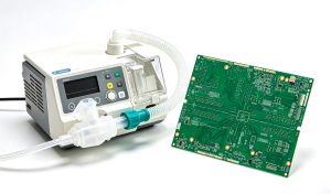
Medical Device Rapid Validation
- Ideal for ECG machines, ultrasound diagnostic devices, and ventilators. Barebones PCB enables 48-72 hour rapid prototyping via minimalist structure and laser/3D printing, reducing costs by 30%-50%. It meets medical-grade requirements for corrosion resistance, low noise, and high precision, such as 0.1mm resolution signal stability in ultrasound probes.
Aerospace Testing Modules
- Suitable for satellite and spacecraft test platforms. Its solder-mask-free design integrates high-temperature ceramic-resin composite substrates, maintaining electrical stability in -40°C to 125°C environments. Supports high-frequency signal validation (e.g., 5G millimeter-wave radar modules), cutting R&D cycles by 50% compared to traditional processes.
Consumer Electronics Iterative Development
- Ideal for smartphones and wearables. 2/4-layer boards with 1-5 day delivery support flexible PCB designs for foldable phone camera modules at 0.1mm thickness, withstanding over 10,000 folding cycles.
Industrial Control Small-Batch Production
- Applied to PLCs and frequency inverters. Standardized manufacturing ensures stable electrical performance, compatible with -20°C to 85°C temperature ranges and 10-2000Hz vibration resistance. Modular designs in industrial robot joint control modules minimize downtime through replaceable components.
5G/Automotive Radar High-Frequency Modules
- For 5G base station RF units and 77GHz automotive millimeter-wave radar. Integrates Rogers RO4450F high-frequency materials with dielectric constant stable at 3.5±0.05 and signal loss as low as 0.004, enabling >10Gbps data transmission. AOI/X-ray inspections ensure batch consistency.
Automotive-Grade Electronic Validation
- Used in automotive controllers and ADAS modules. Adopts FR-408 substrate (Tg≥180°C) and automotive-grade copper foil (1-2oz), meeting AEC-Q200 certification. Impedance deviation remains ≤±2% during -40°C to 125°C thermal cycling, complying with ISO 26262 functional safety standards.
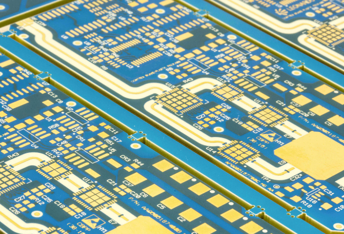
Barebone Circuit Board Technical Specification
| Technical Parameters | Specification |
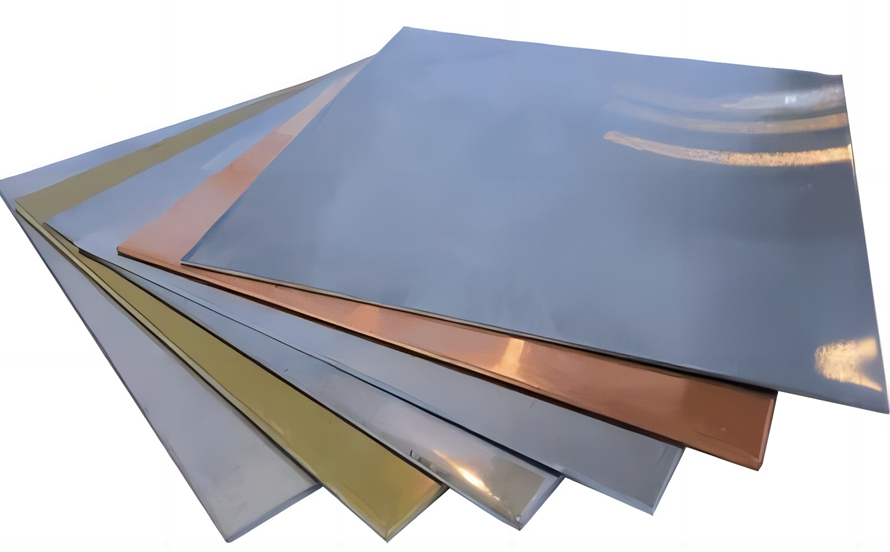
| Substrate Material | FR-4 (Default) / High-Frequency Substrate (Optional) |
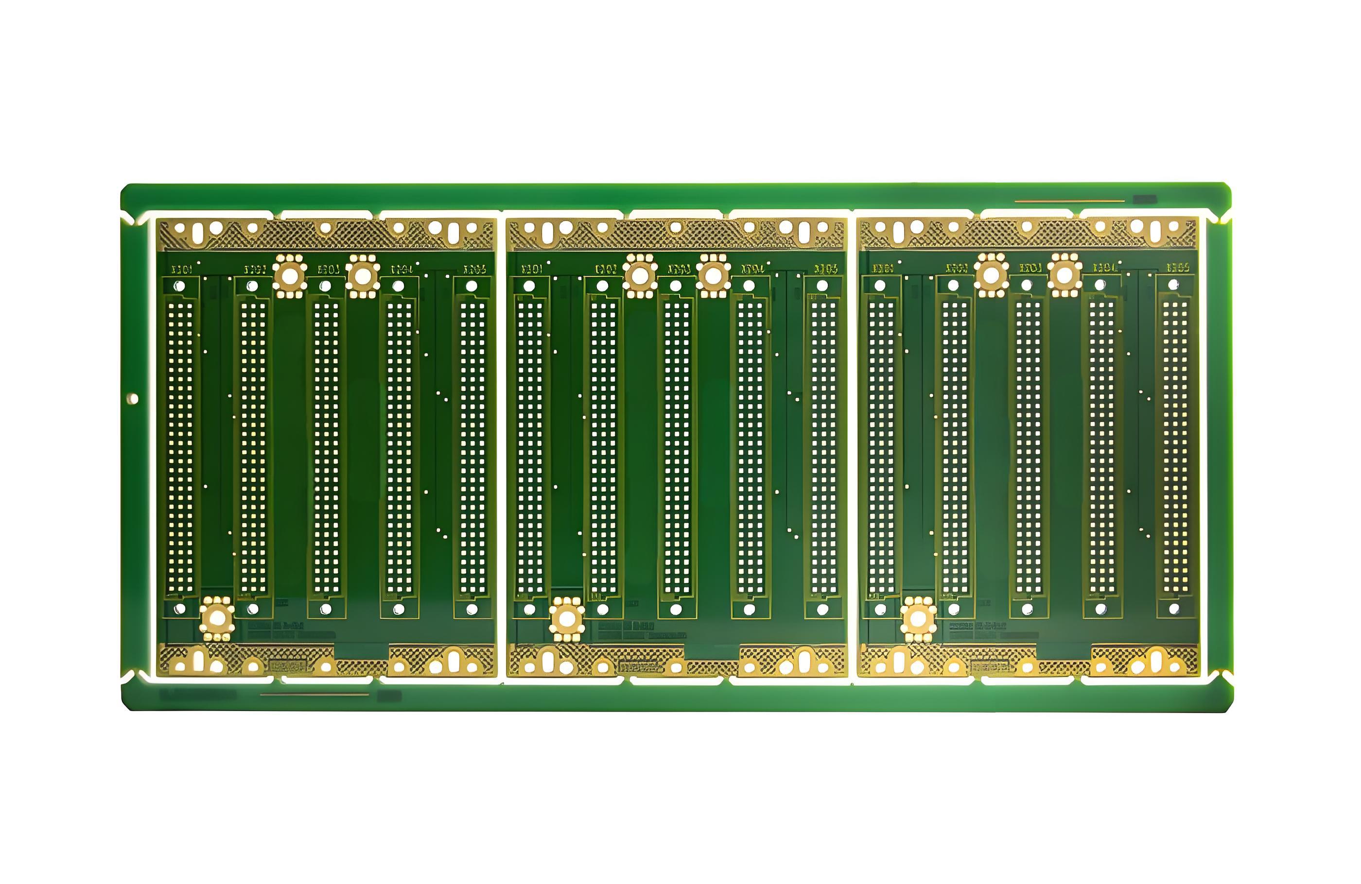
| Layer Count | 2-16 Layers (Typical 4/6 Layers) |
| Copper Thickness | Outer Layer 1oz / Inner Layer 0.5-3oz |
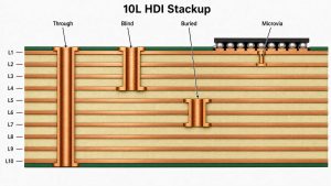
| Trace Width/Spacing | Standard 4/4mil / HDI 2/2mil |
| Hole Type | Mechanical Drill (≥0.3mm) / Laser Microvia |
| Surface Finish | HASL/ENIG/OSP (Select One) |
| Impedance Control | ±10% (Default) / ±7% (High-Speed Requirements) |
| Solder Mask/Silkscreen | LPI Solder Mask (Green Default) |
| Test Requirement | Flying Probe Test |
| Delivery Standard | IPC-A-600G Class 2/3 |
How to Design a Barebones PCB?
Below is a Barebones PCB Design Guide:
1. Define Design Objectives and Parameters
- Identify functional requirements: Clarify the basic functions the PCB needs to achieve (e.g., power distribution, signal transmission), such as “Provide 5V power supply, 3.3V voltage regulation, clock circuit, and reset circuit for a microcontroller minimum system.”
- Set electrical parameters: Determine key parameters based on functional requirements, such as operating voltage (5V/3.3V), current capacity (e.g., max 1A), signal frequency (e.g., 12MHz clock signal), and impedance matching requirements (e.g., 90Ω for USB differential lines).
- Select package types: Choose standard packages based on component availability, such as 0805/0603 for SMD resistors and capacitors, SOIC/QFP for ICs, and 2.54mm pin headers for connectors.
2. Schematic Capture
- Create project file: Use EDA tools (e.g., Altium Designer/Kicad) to create a new project and set the schematic document size (e.g., A4).
- Import component libraries: Add commonly used component libraries (e.g., resistors, capacitors, crystals, power chips) and ensure schematic symbols match their footprints.
- Draw circuit schematics:
- Power section: 5V input → fuse → diode bridge rectifier → filter capacitors (100μF electrolyytic + 0.1μF ceramic) → 3.3V regulator (e.g., AMS1117) → output capacitors.
- Signal section: Microcontroller minimum system (e.g., STC89C52) → clock circuit (12MHz crystal + 22pF load capacitors) → reset circuit (10kΩ pull-up resistor + 10μF capacitor).
- Interface section: Reserve pin headers for programming/debugging (e.g., TXD/RXD, IO pins) and add decoupling capacitors (0.1μF) near power pins.
- Check schematics: Use Electrical Rule Check (ERC) tools to verify connection correctness, ensuring no floating pins, shorts, or unconnected power/ground.
3. PCB Layout Design
- Import netlist: Synchronize the netlist generated from the schematic into the PCB file.
- Plan layer structure: Choose a 2-layer (signal + power/ground) or 4-layer (signal + power + ground + signal) board based on complexity; Barebones typically uses 2-layer boards.
- Layout rules:
- Functional partitioning: Power zone, digital zone, analog zone (if applicable), and interface zone.
- Component placement: Prioritize connectors and large components (e.g., electrolyytic capacitors), then smaller components (e.g., resistors/capacitors). Align IC chips centrally with consistent pin orientation.
- Thermal considerations: Add copper pours and thermal vias under high-power components (e.g., voltage regulators) to avoid heat concentration.
- Layout verification: Check component spacing (e.g., ≥0.3mm to prevent shorts) and ensure no overlaps or board frame breaches.
3. Routing and Rule Setup
- Set routing rules:
- Trace width: ≥20mil for power traces (1A current), ≥8mil for signal traces, 10mil for differential pairs (e.g., USB) with length matching error ≤50mil.
- Clearance: Trace-to-trace ≥8mil, trace-to-pad ≥10mil, pad-to-pad ≥10mil.
- Vias: Inner diameter ≥12mil, outer diameter ≥24mil.
- Manual routing:
- Prioritize critical signals (e.g., clocks, differential pairs) with short, straight paths; avoid 90° right angles (use 45° or curved traces).
- Power/ground: Use thick traces (≥30mil) and copper pours; ensure a complete ground return path to minimize ground bounce noise.
- Decoupling capacitors: Place near IC power pins to shorten return paths.
- Auto-routing assistance: Enable auto-routing for simple designs but manually adjust critical nets.
4. Copper Pouring and Grounding
- Copper pour areas: Use Polygon Pour tools to fill unused areas with ground planes (GND network).
- Thermal copper pours: Add copper pours and thermal vias (2-3 per cm²) under high-power components, connected to the ground plane.
- Isolation and connection: Isolate digital and analog zones (if applicable) with slots and connect grounds via 0Ω resistors or ferrite beads.
- Design Rule Check (DRC)
- Run DRC: Use EDA tools’ DRC function to check trace width, clearance, shorts/opens, and ensure compliance with design rules.
- Correct errors: Adjust spacing or fix unconnected nets based on the DRC report.
5. Generate Manufacturing Files
- Gerber files: Export layer-specific Gerber files (top, bottom, silkscreen, solder mask) in millimeters with ±0.1mm precision.
- Drill files: Export Excellon-format drill files and drill charts with all via/pad positions and dimensions.
- BOM generation: Export a Bill of Materials (BOM) listing component models, footprints, and quantities for procurement and assembly.
- Assembly drawings: Generate PDF assembly drawings with component placement, polarity, and special requirements (e.g., heatsink installation).
6. Verification and Test Preparation
- Simulation validation: Simulate critical circuits (e.g., power, clocks) to ensure stable voltage and signal integrity.
- Design for Manufacturing (DFM): Check minimum trace width/clearance and pad dimensions against PCB fabricator capabilities (e.g., min 6mil trace width).
- Test point design: Add test points (pads or vias) at critical nodes (e.g., power, signal inputs) for debugging.
7. Fabrication and Assembly
- Select fabricator: Choose a PCB manufacturer supporting Barebones processes based on design requirements (e.g., layer count, trace width); provide Gerber files and process specifications (e.g., surface finish: HASL/ENIG).
- Component procurement: Source components per the BOM, ensuring footprint compatibility and quality certifications (e.g., RoHS).
- Soldering: Perform manual soldering or commission SMT assembly, ensuring correct polarity and solder joint quality (no cold solder).
8. Debugging and Validation
- Pre-power checks: Use a multimeter to verify no shorts (e.g., 5V-to-ground resistance) before power-on.
- Functional testing: Measure key voltages (e.g., 5V, 3.3V) post-power-on; use an oscilloscope to check clock signal waveforms (e.g., 12MHz square wave) and verify communication interfaces (e.g., serial output).
- Troubleshooting: If functional anomalies occur, inspect solder joints, power stability, and signal integrity; use a logic analyzer to capture abnormal signals.
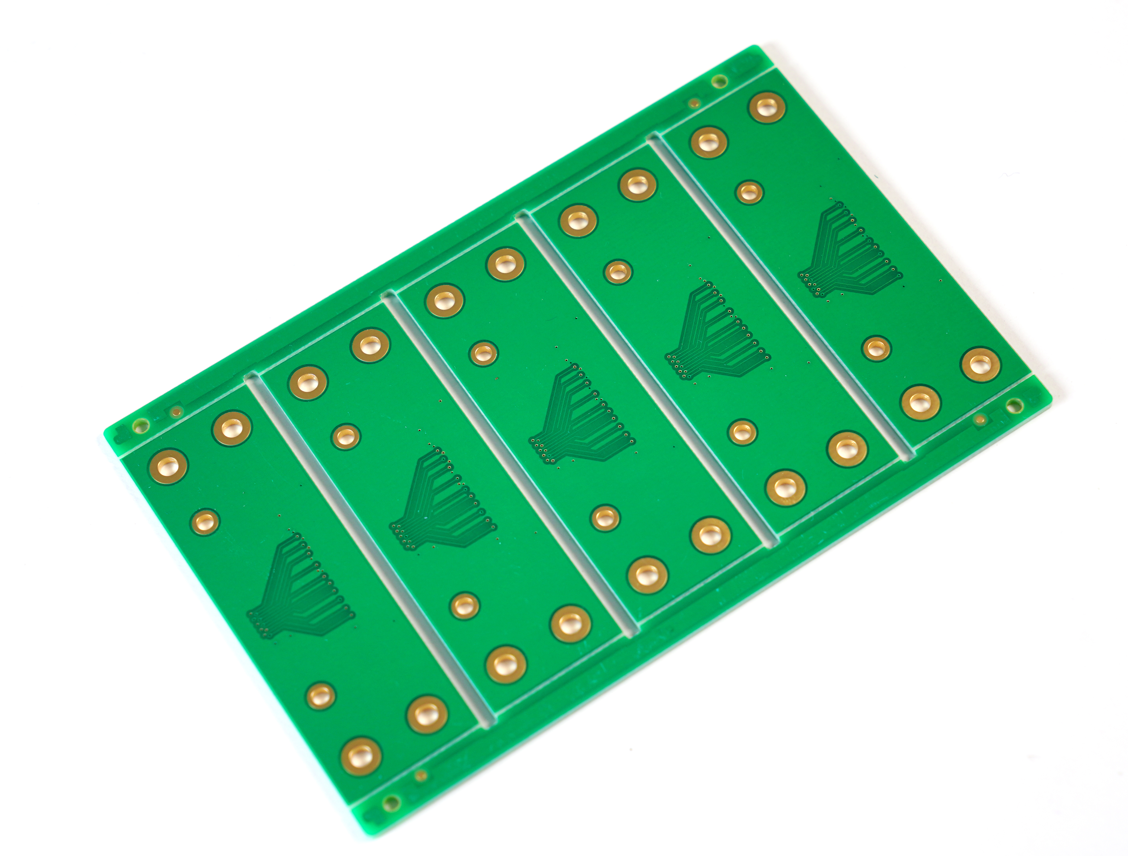
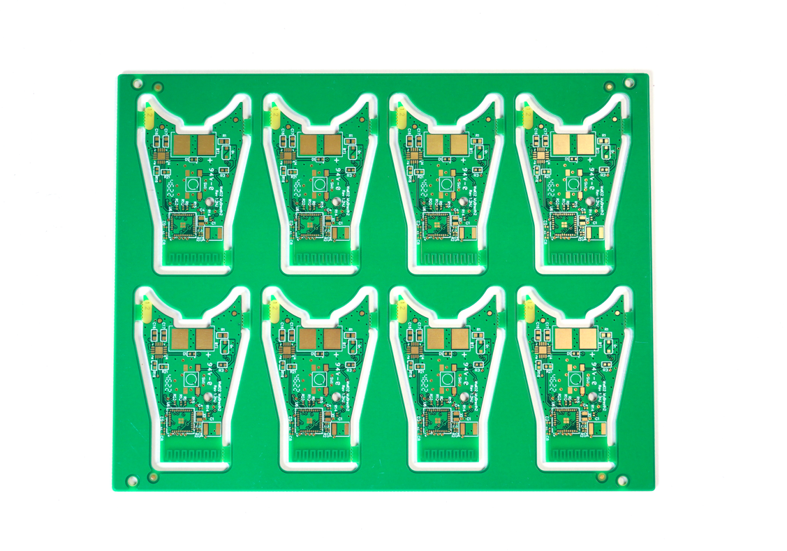
How to Make a Barebones PCB Board?
1. Design File Preparation and Optimization
- Generate Gerber files (including top/bottom/solder mask/silkscreen layers) and Excellon drill files that meet manufacturer requirements. Ensure parameters such as minimum trace width/spacing (e.g., 6mil) and copper thickness (outer layer 1oz, inner layer 0.5-3oz) comply with process capabilities.
- Use DFM software to validate manufacturability, optimize material utilization (e.g., panelization), and confirm alignment with manufacturer’s process parameters (e.g., layer stack symmetry, blind/buried via design).
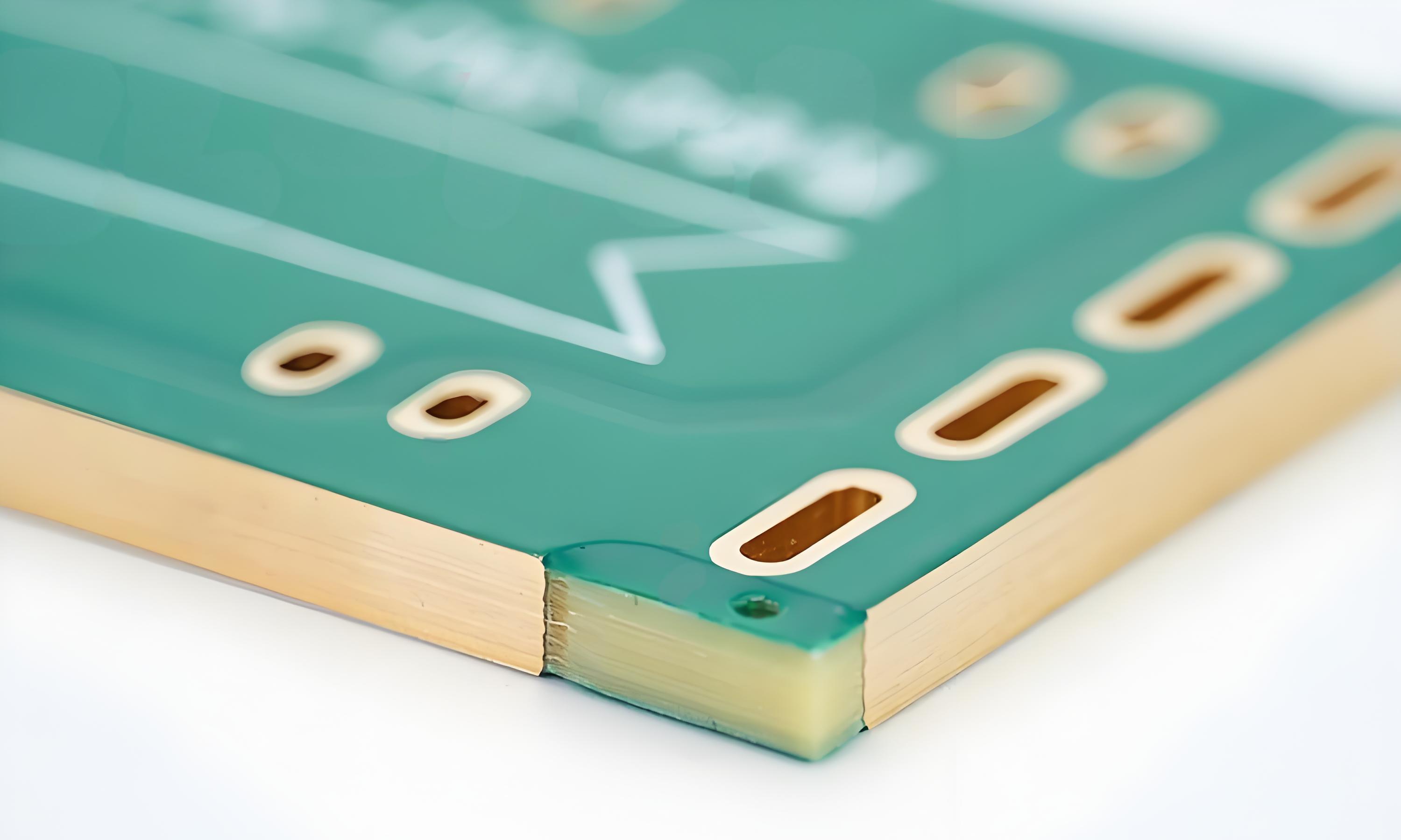
2. Substrate Cutting and Pre-treatment
- Cut raw copper-clad laminate (FR-4 default/high-frequency substrate optional) to design dimensions with edge burrs ≤0.1mm and dimensional tolerance ±0.2mm. Perform baking, edge grinding, and corner rounding to enhance surface roughness.
- Clean copper surfaces to remove oxides and apply micro-etching to improve adhesion of dry/wet film for reliable pattern transfer.
3. Drilling and Hole Metallization
- Use mechanical drilling (≥0.3mm) or laser microvias (≤0.2mm) for through-holes/blind vias with positional accuracy ±0.05mm. Post-drilling, deburr and desmear to eliminate residues.
- Apply electroless copper deposition (0.3-1μm) for hole wall conductivity, followed by panel plating to thicken hole copper to 20-25μm for reliable interlayer electrical connections.
4. Pattern Transfer and Etching
- Lamination: A photosensitive dry or wet film is applied to the copper surface and then applied through heat pressing or coating to form an etch-resistant layer.
- Exposure and Development: The design is transferred to the dry film using ultraviolet light. A developer dissolves the unexposed areas, leaving the remaining dry film as the etch-resistant layer.
- Etching and Stripping: Acidic copper chloride is used to etch the unprotected copper foil, forming the desired circuit. After stripping, a detinning solution is used to remove the tin layer, revealing the final copper circuitry.
5. Solder Mask and Silkscreen Application
- Apply LPI liquid photoimageable solder mask (default green, thickness 15-25μm, window accuracy ±0.1mm) via curtain coating or screen printing.
- Expose and develop to expose pads/holes. Print white silkscreen legends (resolution ≥300dpi, positional tolerance ±0.2mm) for component identification (e.g., part numbers, version codes).
6. Surface Finish Selection
- Select surface finishes (HASL, ENIG, OSP) based on application requirements.
- ENIG is preferred for high-frequency/fine-pitch scenarios, while HASL/OSP is suitable for general use. Ensure compliance with RoHS certification and thermal stability (e.g., Tg≥180°C) for oxidation resistance and solderability.
7. Profiling and Cutting
- Route or laser-cut panels to final dimensions with dimensional tolerance ±0.1mm and smooth edges.
- Use V-cut or die-cutting for SMT compatibility, ensuring no burrs or delamination to meet assembly requirements.
8. Electrical Testing and Quality Inspection
- Perform flying probe testing (100% coverage for opens/shorts, ±10% impedance tolerance) and AOI for visual defects (trace gaps, solder mask bridges).
- Conduct manual/AI visual checks for oil contamination, character clarity, and warpage (≤0.75%).
9. Final Inspection and Packaging
- Execute FQC sampling to verify electrical performance, appearance, dimensions, hole size, and thickness against IPC-A-600G Class 2/3 standards.
- Package in anti-static bags with hardboard backing, include test reports, manuals, and warranty cards for secure delivery.
How Much Does a Barebone PCB Cost?
The price range for bare PCBs abroad is influenced by multiple factors, including the number of layers, material, surface treatment, order quantity, and delivery time. Specific unit prices are as follows:
- Double-sided boards: Large quantities (≥1000 pieces) of standard FR-4 material cost approximately $0.04–$0.06/cm² (thickness ≤1.2mm). Small quantities or expedited orders can cost up to $0.08–$0.12/cm².
- Four-layer boards: Large quantities of standard FR-4 material cost approximately $0.06–$0.09/cm². High-frequency materials (such as Rogers RO5880) or blind and buried via designs can cost up to $0.20–$0.30/cm².
- 6-layer boards: The high-volume unit price of standard FR-4 material is approximately $0.30–$0.50/cm². For HDI processes (line width/space ≤ 3 mil) or high-frequency materials, the price can rise to $1.50–$2.00/cm². Due to the high material cost, 6-layer boards made of Rogers material are priced at approximately $15–$20 per board (based on a 10cm×15cm board).
- 10-layer and higher: The high-volume unit price of standard FR-4 material is approximately $0.35–$0.55/cm². High-frequency materials or designs with 50Gbps signal layers can cost up to $1.00–$2.00/cm². The high-volume cost of a 10-layer board is approximately $75–$100 per board.
The actual price must be determined through negotiation with the supplier based on specific design parameters, order volume, and delivery time. High-end applications (such as 5G base stations and medical equipment) may incur higher costs due to their stringent performance requirements.
Why Choose EBest Circuit (Best Technology) as Barebones PCB Manufacturer?
Reasons Why Choose Us as Barebones PCB Manufacturer:
- Price Competitiveness Service: Deliver cost-sensitive solutions through optimized design cost structures, achieving 15%-20% unit cost reduction via scaled procurement and process improvements, directly enhancing budget control and procurement confidence.
- Rapid Prototyping Service: Enable 24-hour quick-turn prototyping, completing full-cycle design-to-delivery within 48 hours for urgent orders, accelerating time-to-market and strengthening market first-mover capabilities.
- On-Time Delivery Service: Achieve 99.2% on-time delivery rate with intelligent production scheduling and dynamic inventory management, minimizing project risks from delays and reinforcing supply chain reliability.
- Stringent Quality Control Service: Implement 100% batch inspection with six-stage quality checkpoints (raw material intake to final shipment), coupled with AOI optical inspection and flying probe testing, ensuring defect rates below 0.03% and solidifying quality trust.
- Certification Compliance Service: Hold globally recognized certifications including ISO 9001, IATF 16949, medical-grade ISO 13485, and RoHS 2.0, providing authoritative compliance backings for automotive, medical, and industrial sectors to lower market entry barriers.
- Experience-Driven Database Service: Leverage a 19-year PCB production error database containing 5,000+ typical process solutions to prevent recurring errors via historical data comparison, directly reducing trial-and-error costs for clients.
- Free DFM Analysis Service: Offer complimentary design-for-manufacturing feasibility analysis to pre-identify design flaws and optimize manufacturability, shortening design iteration cycles by 30% and boosting first-pass design success rates.
- End-to-End Solution Service: Provide seamless one-stop services spanning design collaboration, rapid prototyping, volume production, and functional testing, minimizing client coordination efforts with multiple vendors and ensuring concept-to-product continuity.
- Cost Optimization Support: Reduce hidden costs (rework, scrap) through error database insights and process refinements, combined with volume-based discount policies, achieving 8%-12% additional cost savings and enhancing long-term partnership value.
- Emergency Response System: Operate a 7×24 rapid-response team with green-channel prioritization for special orders, ensuring 4-hour solution feedback and dedicated account management to elevate emergency handling trust and client satisfaction.
Welcome to contact us if you have any request for barebones PCB board: sales@bestpcbs.com.