PCB manufacturing PCB manufacturing
Home > Blog

PCB

What Is led light pcb?
Friday, August 2nd, 2024

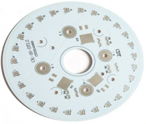
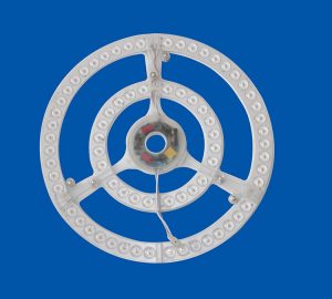
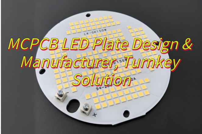
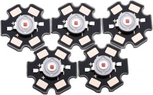
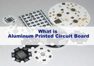
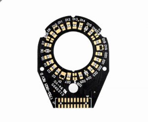
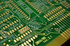
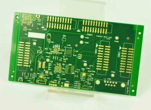
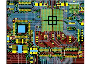
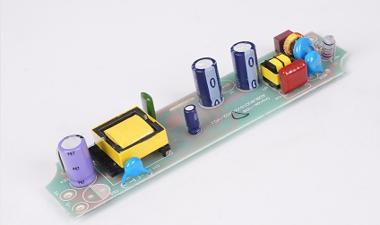
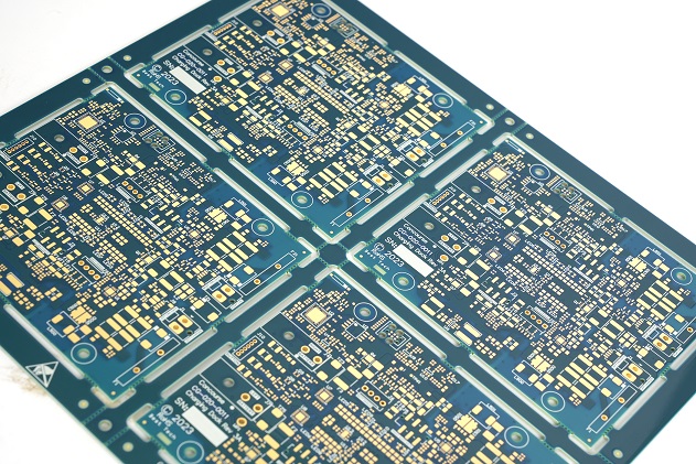
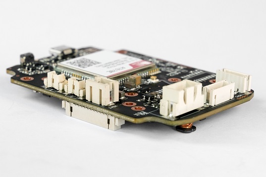
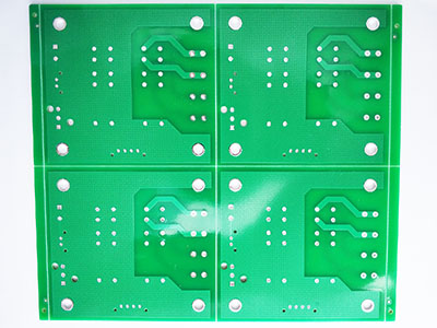
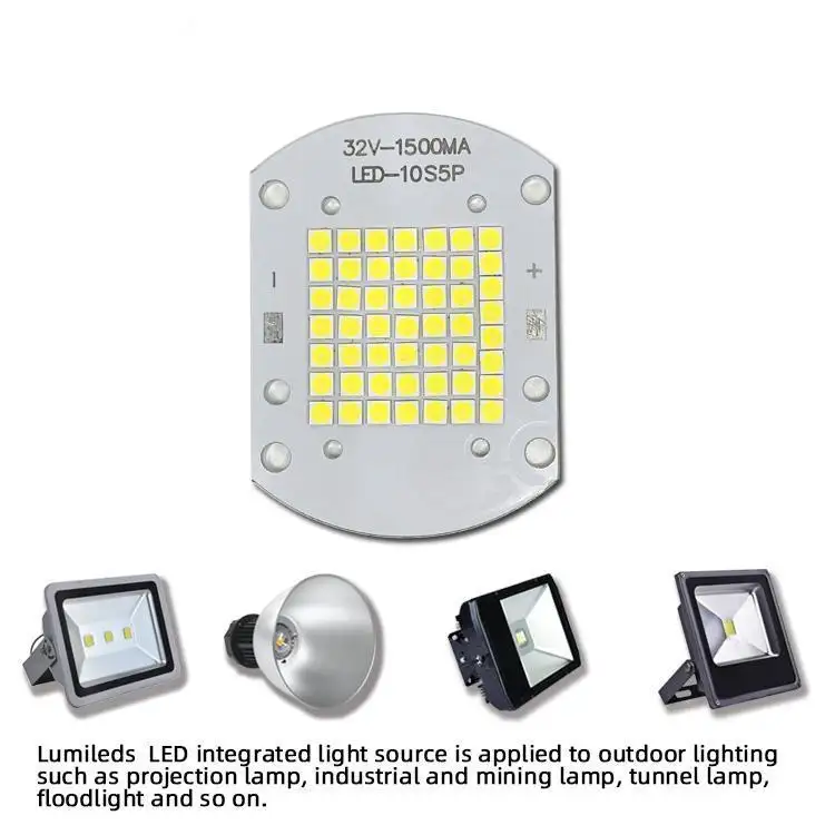
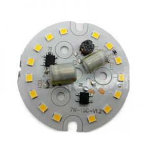
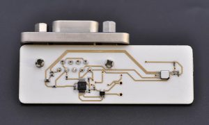
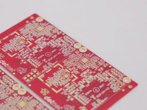
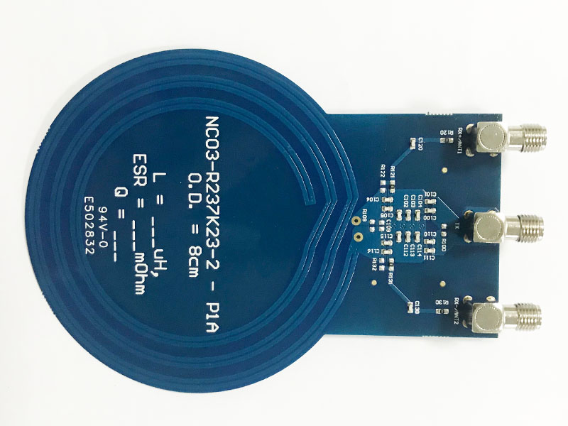
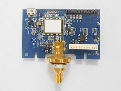
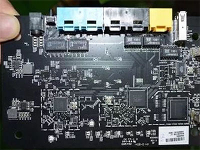
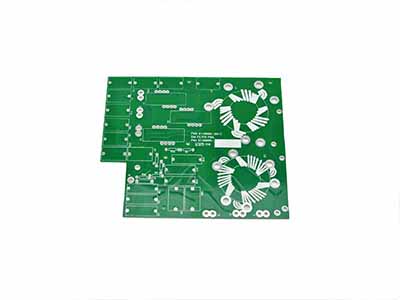
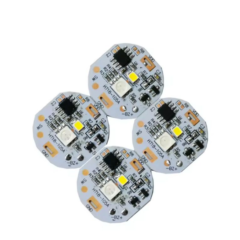
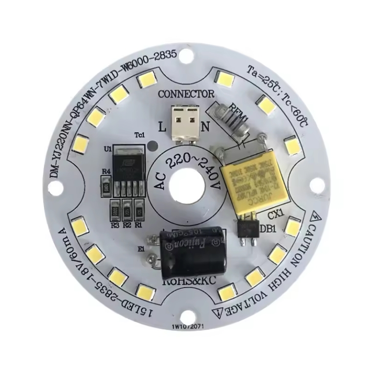
led light pcb , or printed circuit board, is a stable carrier of electronic components. It not only realizes electrical connection but also plays a supporting role. As the core component of electronic products, it is widely used in various electronic devices. In the field of LED lighting, PCB light board provides support and power for LED lamp beads, ensuring their stable operation in scenes such as home, commercial and automotive lighting. PCB with LED is often used to manufacture electronic products such as indicator lights, lighting equipment and display screens. The LED lamp beads on these PCBs are usually precisely soldered by SMT (surface mount technology).
What Is led light pcb?

led light pcb

LED PCB light board leads the development of the lighting industry with its innovative design, high efficiency and flexibility, bringing a more intelligent and comfortable lighting experience to our lives. It is not only an integrated platform for electronic components, but also a perfect combination of modern technology and aesthetics, and is the focus of future lighting trends.

Why use mcpcb for led light pcb

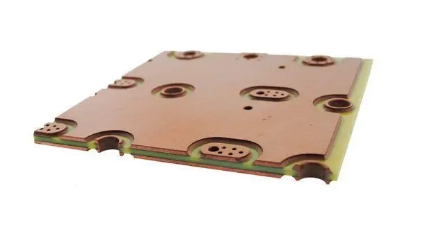
With the continuous development of LED technology, the heat generated by LEDs has gradually increased. The traditional FR4 printed circuit board (PCB) has been unable to meet the heat dissipation requirements due to its low thermal conductivity (only 0.36W/m.K). In order to solve this problem, the metal core printed circuit board (MCPCB) was proposed. It attaches the original printed circuit board to a metal with better thermal conductivity (such as aluminum and copper) to enhance the heat dissipation effect. The thermal conductivity efficiency of MCPCB is higher than that of traditional FR4 PCB, reaching 1W/m.K to 2.2W/m.K, which effectively improves the heat dissipation performance of LED PCB.

In addition, the use of MCPCB can also reduce the number of LEDs required to generate lighting, making it an ideal choice for street lights, automotive LED applications, and backlight unit applications. The use of metal substrates has practical advantages in heat dissipation, thermal conductivity, reliability, and electrical insulation, especially in harsh environments, and can also achieve reliable operation of LEDs. For example, using a metal substrate can reduce the LED junction temperature by 20-30°C, improve light output and enhance the overall performance of the product, ensure consistent UV light generation, and expand the possibilities of UV applications in various industries.
Why use mcpcb for led light pcb

Why use mcpcb for led light pcb

Advantages of led light pcb?

High thermal conductivity: LED PCB, especially aluminum substrate, uses aluminum alloy material with high thermal conductivity, which can effectively conduct away the heat generated by LED, maintain the stability of LED operation and extend the service life. This high thermal conductivity is essential to prevent heat accumulation and keep LED working at high brightness for a long time.

High efficiency: Compared with traditional incandescent lamps and energy-saving lamps, LED lamps have higher luminous efficiency and can provide better lighting effects while reducing energy consumption. This makes LED PCB have significant advantages in energy saving and environmental protection.

Long life: The service life of LED PCB far exceeds that of traditional lighting products, and it can provide longer continuous lighting, reducing the trouble of frequent bulb replacement and reducing maintenance costs.

Low energy consumption: LED PCB requires much less electricity than traditional lighting equipment while providing the same brightness, which is very important for energy saving, emission reduction and sustainable development

How does led light pcb dissipate heat?

The power device is mounted on the circuit layer. The heat generated by the device during operation is quickly transferred to the metal base layer through the insulating layer, and then the metal base layer transfers the heat to achieve heat dissipation of the device. Compared with the traditional FR-4, the aluminum substrate can reduce the thermal resistance to the minimum, making the aluminum substrate have excellent thermal conductivity; compared with the thick film ceramic circuit, its mechanical properties are extremely good. In the circuit design scheme, the heat diffusion is handled very effectively, thereby reducing the module operating temperature, extending the service life, and improving the power density and reliability; reducing the assembly of the heat sink and other hardware (including thermal interface materials), reducing the product volume, and reducing the hardware and assembly costs; combining the power circuit and the control circuit

How to make a LED light circuit board?

  1. Cutting
  2. Cutting process Picking materials – cutting
  3. The purpose of cutting
    Cut the large-sized incoming materials into the size required for production
  4. Precautions for cutting
    ① Check the size of the first piece of material
    ② Pay attention to the scratches on the aluminum surface and the copper surface
    ③ Pay attention to the delamination and flash of the board edge
  5. Drilling
  6. Drilling process
    Pinning – drilling – board inspection
  7. The purpose of drilling
    Positioning and drilling holes in the board to assist the subsequent production process and customer assembly
  8. Precautions for drilling
    ① Check the number of holes and the size of the holes
    ② Avoid scratches on the board
    ③ Check the flash of the aluminum surface and the hole position deviation
    ④ Check and replace the drill bit in time
    ⑤ Drilling is divided into two stages, one drilling: drilling holes after cutting for peripheral tool holes
    Second drilling: tool holes in the unit after solder mask
  9. Dry/wet film imaging
  10. Dry/wet film imaging process
    Grinding board – film pasting – exposure – development
  11. Purpose of dry/wet film imaging
    To present the part required for making circuits on the board
  12. Precautions for dry/wet film imaging
    ① Check whether the circuit is open after development
    ② Whether the development alignment is biased to prevent the generation of dry film fragments
    ③ Pay attention to the circuit defects caused by scratches on the board
    ④ No air should remain during exposure to prevent poor exposure
    ⑤ After exposure, it should be still for more than 15 minutes before development
    IV. Acid/alkaline etching
  13. Acid/alkaline etching process
    Etching-film stripping-drying-board inspection
  14. Purpose of acid/alkaline etching
    After imaging the dry/wet film, keep the required circuit part and remove the excess part outside the circuit. During acid etching, attention should be paid to the corrosion of the etching solution to the aluminum substrate;
  15. Precautions for acid/alkaline etching
    ① Pay attention to incomplete etching and excessive etching
    ② Pay attention to line width and line thickness
    ③ Oxidation and scratches are not allowed on the copper surface
    ④ The dry film should be removed cleanly
    V. Silk screen solder mask and characters
  16. Silk screen solder mask and character process
    Silk screen-pre-bake-exposure-development-characters
  17. Purpose of silk screen solder mask and characters
    ① Anti-soldering: protect circuits that do not need soldering and prevent tin from entering and causing short circuits
    ② Characters: serve as markings
  18. Precautions for silk screen solder mask and characters
    ① Check whether there is garbage or foreign matter on the board
    ② Check the cleanliness of the stencil ③ Pre-bake for more than 30 minutes after silk screen printing to avoid bubbles in the circuit
    ④ Pay attention to the thickness and uniformity of the silk screen
    ⑤ After pre-bake, the board should be completely cooled to avoid film contamination or damage to the glossiness of the ink surface
    ⑥ Place the ink side down during development
    VI. V-CUT, gong board
  19. V-CUT, gong board process
    V-CUT——gong board——tear protective film——remove burrs
  20. Purpose of V-CUT, gong board
    ① V-CUT: Cut the single PCS circuit and the entire PNL board to leave a small part connected for easy packaging and removal
    ② Gong board: remove the excess part of the circuit board
  21. Precautions for V-CUT, gong board
    ① During the V-CUT process, pay attention to the size of the V, the incompleteness and burrs of the edges
    ② Pay attention to the burrs caused by the gong board, the gong knife is tilted, and the gong knife is checked and replaced in time
    ③ Finally, avoid scratches on the board when removing the burr
    VII. Testing, OSP
  22. Testing, OSP process
    Circuit test-voltage resistance test-OSP
  23. Testing, the purpose of OSP
    ① Circuit test: Check whether the completed circuit is working normally
    ② Voltage resistance test: Check whether the completed circuit can withstand the specified voltage environment
    ③ OSP: Allow the circuit to be soldered better
  24. Testing, OSP precautions
    ① How to distinguish and store qualified and unqualified products after testing
    ② Placement after OSP
    ③ Avoid damage to the circuit
    VIII. FQC, FQA, packaging, shipment
  25. Process
    FQC-FQA-packaging-shipping
  26. Purpose
    ① FQC conducts full inspection and confirmation of the product
    ② FQA spot check and verification
    ③ Pack and ship to customers as required
  27. Note
    ① FQC should pay attention to the appearance confirmation during the visual inspection and make reasonable distinctions
    ② FQA should conduct random inspections to verify the inspection standards of FQC
    ③ Confirm the packaging quantity to avoid mixed boards, wrong boards and packaging damage

Capabilities of led light pcb?

ItemCapabilities
Layer Count1 – 10 Layers
Max Board Dimension24*64″(610*1625mm)
Min Board Thickness0.6mm
Max Board Thickness4.0mm
Conductor Thickness0.5oz – 10oz
Min Line Width/Line Space4/4mil (0.10/0.10mm)
Min Hole Diameter10mil (0.25mm)
Min Punch Hole Dia0.12″ (3.0mm)
Min Hole Spacing16mil (0.4mm)
Min PAD Ring(Single)3mil (0.075mm)
PTH Wall ThicknessNormal: 0.59mil (15um); HDI: 0.48mil (12um)
Min Solder PAD Dia14mil (0.35mm)
Min Soldermask Bridge8mil (0.20mm)
Min BAG PAD Margin5mil (0.125mm)
PTH/NPTH Dia TolerancePTH: ±3 mil (0.075mm); NPTH: ±2mil (0.05mm)
Hole Position Deviation±3mil (0.075mm)
Outline ToleranceCNC: ±6 mil (0.15mm); Die Punch: ±6 mil (0.1mm)
Max Aspect Ratio10:01
Surface TreatmentENIG, Flash Gold, Hard Gold Finger, Gold Plating(50mil), Gold finger,
Selected Gold Plating, ENEPIG, ENIPIG, HAL, HASL(LF), OSP, Silver Imm., Tin Imm

Applications of led light pcb?

  1. Application in medical equipment
    The rapid progress of medicine is closely related to the rapid development of the electronics industry. Many medical devices are made of basic PCBs alone, such as pH meters, heart rate sensors, temperature measurements, electrocardiographs, electroencephalographs, MRIs, X-ray machines, CT scanners, blood pressure machines, blood sugar level measuring equipment, etc.
  2. Application in industrial equipment
    PCBs are widely used in manufacturing, especially in industries with high-power mechanical equipment; these devices run on high power and require high current circuit drive. Such as arc welding, large servo motor drives, lead-acid battery chargers, clothing cotton machines, etc.
  3. Application in lighting
    LED lights and high-intensity LEDs are mounted on PCBs based on aluminum substrates; aluminum has the property of absorbing heat and dissipating it in the air.
  4. Application in the automotive and aerospace industries
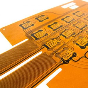
    Flexible PCBs are lightweight but can withstand high vibrations. Because of their light weight, they can reduce the total weight of spacecraft; flexible PCBs can be adjusted even in narrow spaces. These flexible PCBs are used as connectors, interfaces, and can be assembled even in compact spaces

You may also like

What is a heavy copper PCB?
Wednesday, July 31st, 2024

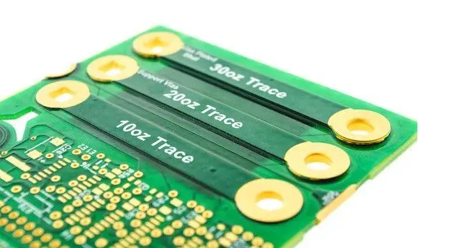
Heavy Copper Board does not have a set of definition per IPC. According to PCB industry, however, peopel generally use this name to identify a printed circuit board with copper conductors 3 oz/ft2 – 10 oz/ft2 in inner and/or outer layers. And Extreme heavy copper PCB refers to 20 oz/ft2 to 200 oz/ft2 printed circuit board.

What is a heavy copper PCB?

Heavy copper normally used for a various products but not limited to: high power distribution, heat dissipation, planar transformers, power convertors, and so on.

Generally, the thick copper plate is about 3oz, and the larger current is 3oz~6oz. To achieve 15 ounces, the requirements for process and manufacturers are more stringent. Best provides 3-15oz 1-99 layers of PCB. It is a professional PCB manufacturer with 18 years of experience, providing one-stop PCB and PCBA services from design, manufacturing to after-sales.

Common copper foil thicknesses have the following options:

  1. 1 oz (35 μm): This is the most common and standard copper foil thickness, widely used in general electronic product manufacturing. It has good electrical and thermal conductivity.
  2. 2 oz (70 μm): This thickness of copper foil is usually used in circuits that require higher current carrying capacity, such as power amplifiers, high-power LEDs, etc.
  3. 0.5 oz (18 μm): This thinner copper foil thickness is suitable for some light and small electronic products, such as electronic watches, mobile phones, etc.
  4. Other thicknesses: According to special needs, you can also choose copper foil of other thicknesses, such as 3 oz, 4 oz, etc.

What is copper foil

Copper foil is a cathodic electrolytic material, a thin, continuous metal foil deposited on the substrate layer of the circuit board, which serves as the conductor of the PCB. It is easy to adhere to the insulating layer, accept the printed protective layer, and form a circuit pattern after corrosion. The copper mirror test is a flux corrosion test, using a vacuum precipitation film on a glass plate. Copper foil is made of copper and a certain proportion of other metals. Copper foil generally has two types: 90 foil and 88 foil, that is, the copper content is 90% and 88%, and the size is 16*16cm.

How thick is the PCB copper foil

The commonly used international PCB copper foil thicknesses are: 35um, 50um, and 70um.
Generally, the thickness of copper foil (copper cladding) of single-sided and double-sided PCB boards is about 35um (1.4mil), and the other specifications are 50um and 70um.
The surface thickness of multilayer boards is generally 35um=1oz (1.4mil), and the inner layer is 17.5um (0.7mil). 70% of circuit boards use a copper foil thickness of 35um, which mainly depends on the purpose of the PCB and the voltage and current of the signal; in addition, for PCBs that need to pass large currents, some will use 70um copper thickness, 105um copper thickness, and rarely 140um, etc. The copper foil thickness is usually expressed in oz (ounces). 1oz refers to the thickness of 1oz of copper evenly covering an area of ​​1 square foot, which is about 1.4mil. It uses the weight per unit area to express the average thickness of the copper foil.
Expressed in formula, that is, 1oz=28.35g/ FT2 (FT2 is square feet, 1 square foot = 0.09290304 square meters).

What is a heavy copper PCB?

Different uses have different copper foil thicknesses,

  1. Ordinary 0.5oz, 1oz
  2. 2oz, mostly used in consumer and communication products.
    Thick copper products above
  3. 3oz are mostly used for large currents, such as high-voltage products and power boards!

Copper foil thickness (track width) affects the current size. Although there is a formula that can directly calculate the current load capacity of copper foil, it is not so simple when actually designing the circuit. Therefore, safety should be fully considered when designing.

How thick is 2 oz of copper for PCB?

In the PCB industry, 1OZ means the thickness of 1OZ of copper evenly laid on an area of ​​1 square foot (FT2). It uses the weight per unit area to express the average thickness of the copper foil. Expressed in formula, 1OZ=28.35g/FT2 (FT2 is square feet, 1 square foot=0.09290304 square meters).
First, we know that the density constant of copper and the conversion formula of related units are as follows:
1 cm = 10 mm; 1 mm = 1000 um
1 FT2≈929.0304cm2
According to the mass calculation formula m=ρ×V(volume)=ρ×S(area)×t(thickness), we know that the weight of copper foil divided by the density and area of ​​copper is the thickness of copper foil!
So, t=28.35÷929.0304÷8.9cm≈0.0034287cm=34.287um≈34.287÷25.4mil≈1.35mil
Copper thickness 1.OZ(0.035mm) Copper thickness 1.5OZ(0.05mm) Copper thickness 2.OZ (0.07mm)

What are the materials of PCB board

FR-1——phenolic cotton paper, this base material is commonly known as bakelite (more economical than FR-2)
FR-2——phenolic cotton paper
FR-3——cotton paper, epoxy resin
FR-4——glass cloth, epoxy resin
FR-5——glass cloth, epoxy resin
FR-6——matte glass, polyester
G-10——glass cloth, epoxy resin
CEM-1——cotton paper, epoxy resin (flame retardant)
CEM-2——cotton paper, epoxy resin (non-flame retardant)
CEM-3——glass cloth, epoxy resin
CEM-4——glass cloth, epoxy resin
CEM-5——glass cloth, polyester
AIN——aluminum nitride
SIC——silicon carbide

You may also like

What is a Zero PCB Board? – EBest Circuit (Best Technology)
Wednesday, July 24th, 2024

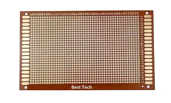
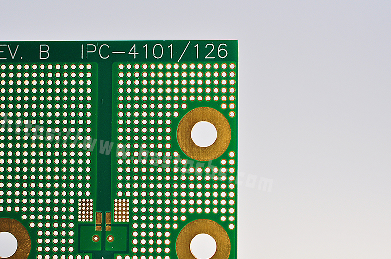
A zero PCB, also known as a prototype PCB or breadboard, is a type of circuit board used for building and testing prototypes. Unlike traditional PCBs, which have pre-defined paths for electric connections, zero PCBs offer a grid of holes. This grid allows for custom circuit designs using wires and components. Engineers and hobbyists use zero PCBs to experiment and develop new electronic circuits without committing to a specific design.

What is a zero PCB?

Zero PCBs are particularly helpful in testing circuit designs for any shortcomings. They provide a cost-efficient way to evaluate the circuitry before committing to a final solution. The term ‘zero’ in this context signifies a fundamental distinction. It implies that there are no predefined connections, layouts, or functions on the PCB.

What is a Zero PCB Board? - EBest Circuit (Best Technology)

Generally, there is no solder mask and silkscreen on the zero board. The primary purpose of a zero PCB is to offer a blank canvas for users to create and test custom circuits. As a result, they are intentionally kept simple in structure to allow for maximum customization. Users are free to design and solder their circuits and components directly onto the board without the constraints of a predefined layout or solder mask.

What is the use of a zero board?

Zero boards serve a variety of purposes in the electronics industry. They are particularly useful for prototyping and testing new circuit designs. Here are some common uses:

  • Prototyping
  • Educational purposes
  • Quick fixes
  • Small-scale production

Zero PCBs have a layer of copper traces or pads on the substrate. These copper elements provide the conductive pathways for soldering electronic components and forming connections. However, the copper traces on zero PCBs are usually unconnected, meaning there is no predefined circuit layout. You can build a circuit on them by inserting components into the holes and then connecting them with wires.
What is the cost of a zero PCB board?
The cost of zero PCB boards varies based on size, material, and supplier. Generally, they are quite cost-effective, so that both professional engineers and hobbyists can afford it. Prices can range from a few cents for small boards to several dollars for larger or more specialized versions. Bulk purchasing often reduces the cost per unit. Additionally, different materials, such as fiberglass or phenolic, can affect the price.

What size is a zero PCB board?

Zero PCB boards come in various sizes to accommodate different project needs. Common sizes include:

  • Small: Typically around 5×7 cm, ideal for simple projects.
  • Medium: Sizes like 10×15 cm offer more space for complex circuits.
  • Large: Boards as large as 30×30 cm are available for extensive projects.

The grid pattern usually remains consistent, with a standard pitch of 2.54 mm (0.1 inches) between holes, regardless of the board’s overall size.

What is a bare board?

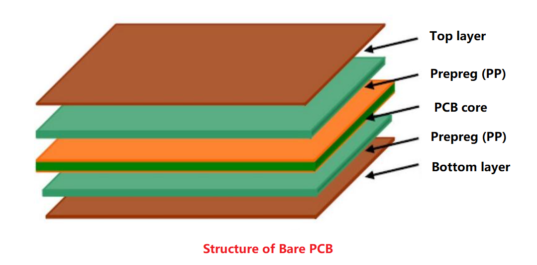
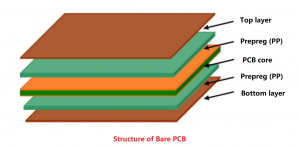
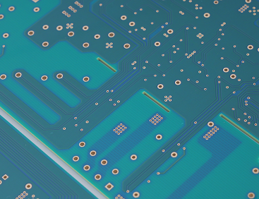
A bare board, also known as a blank PCB, is a printed circuit board that has not yet been populated with any electronic components. It is essentially the foundation of a PCB, consisting only of the substrate material (such as fiberglass) and the copper traces that form the circuit pathways. A bare board typically include base core, prepreg and copper trace layer.

What is a Zero PCB Board? - EBest Circuit (Best Technology)

Features of a bare board

  • Substrate material

The base material of a bare board is usually fiberglass, FR4, or other insulating materials that provide mechanical support.

  • Copper traces

These are the conductive pathways etched onto the substrate. They form the circuit’s electrical connections but are not yet connected to any components.

  • Pads and holes

Bare boards include pads (flat areas of copper for soldering components) and drilled holes for through-hole components.

  • Pre-defined layout

The copper traces and pads are arranged according to a specific design, determined during the PCB design process.

  • No components

A bare board does not have any electronic components soldered onto it yet. It is essentially a “blank slate” ready to be populated.

  • Coated solder mask and silkscreen

Most bare boards have a solder mask, a protective layer that prevents solder from bridging between conductive areas, and a silkscreen, which provides component labels and other information.

If you are looking for a reliable supplier for your PCB needs, consider companies like EBest Circuit (Best Technology), who is known for their quality and customer service. EBest Circuit (Best Technology) offers a range of options to support your electronic projects from prototyping to production. Contact us right now to get your quotation.

You may also like

PCB vs CCA: What is a Circuit Card Assembly?
Monday, July 22nd, 2024

Hey there! If you’re curious about circuit card assembly (CCAs) and what makes them tick, you’ve come to the right place. CCAs are the unsung heroes behind many of the electronic devices we use every day. Let’s dive into what they are, their essential parts, how they’re made, and why they’re so important.

What is a circuit card assembly?

Circuit card assembly or CCA is the process of producing printed circuit boards. In essence, it is the same as PCBA (PCB assembly), just in different name. CCA is a manufacturing technology that converts raw materials into printed circuit boards. It is used in many industries, including the military and aerospace sectors. This type of manufacturing requires skilled professionals to lay out the design and then assemble it. If you are planning to buy a batch of circuit card components, here are some things you should know about CCA.

PCB vs CCA: What is a Circuit Card Assembly?

A circuit card is a thin, flat dielectric material on which conductive paths or traces are etched. These paths connect various electronic components. They are also used to connect components to sockets on printed circuit boards. Circuit card assy is the process of manufacturing circuit card components. The process involves adding electronic components to the substrate.

Key components of a circuit card assembly (CCA)

Circuit card assembly have several key components to make the circuit function properly. These can be divided into three basic components.

  • Printed Circuit Board (PCB)
  • Electronic component
  • Solder paste
  • Printed Circuit Board (PCB)

This is the backbone of the CCA. The printed circuit board provides the structural foundation on which all other components are mounted. A PCB is typically made of a flat, insulating material such as FR4 fiberglass, which is layered with conductive tracks made of copper. These tracks form the circuit pathways that connect various electronic components. The PCB board can be single-sided, with components and conductive tracks on one side only, or double-sided, with tracks and components on both sides. For more complex applications, multi-layer PCBs are used, which consist of multiple layers of insulating material and conductive pathways stacked together. These printed circuit boards are essential in ensuring that electrical signals are routed efficiently and reliably across the assembly.

PCB vs CCA: What is a Circuit Card Assembly?

  • Electronic Components

These include resistors, capacitors, integrated circuits, transistors, and more passive and positive components. Each part plays a specific role in the circuit, like pieces of a puzzle fitting together to make a complete picture. Resistors control the flow of electrical current, capacitors store and release energy, integrated circuits (ICs) perform various functions like processing and memory storage, and transistors act as switches or amplifiers. These components are carefully placed on the PCB in positions that allow them to connect and interact as designed.

PCB vs CCA: What is a Circuit Card Assembly?

  • Solder paste

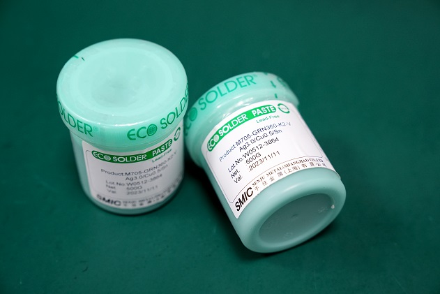
Solder paste is like the glue that holds everything together, but it’s electrically conductive. It’s used to attach the electronic components to the PCB, so that they can stay put and work properly. Soldering creates a strong, conductive bond between the component leads and the PCB’s copper tracks. There are different types of soldering, such as lead-based and lead-free solders, each with its specific properties and applications. The soldering process can be done manually or using automated printing machines, depending on the complexity and volume of the assembly. Please noticed that solder paste should used in a very short time, otherwise, it will become dry solder paste.

PCB vs CCA: What is a Circuit Card Assembly?

What is the Difference Between a PCB and a CCA?

You might wonder, what’s the difference between a PCB and a CCA? Well, here’s a quick rundown:

AspectPCB (Printed Circuit Board)CCA (Circuit Card Assembly)
DefinitionA blank board with conductive pathwaysA PCB populated with electronic components
ComponentsNo electronic componentsIncludes electronic components like resistors, capacitors, ICs
FunctionalityServes as the foundation for electronic circuitsA functional electronic circuit ready for use in devices
Manufacturing StepsInvolves design, etching, and printing of conductive pathsInvolves PCB manufacturing plus component placement and soldering
Usage StageIntermediate stage in manufacturingFinal stage, ready for integration into electronic devices
ComplexityLess complex, involves fewer manufacturing stepsMore complex, involves multiple stages of assembly and testing

What is the circuit card assembly manufacturing process?

Making a CCA is a multi-step process:

Design

First, the PCB layout is designed using computer software. It includes numerous steps, like schematic drawing, layout design, SI, PI analysis, DFM. This can ensure the PCB board can fit all the necessary components and function correctly.

Fabrication

The PCB is then fabricated, which involves creating the physical board with layers of insulating and conductive materials. This is where the board gets its pathways. In this step, proceed strict quality control process to make sure the bare boards are qualified.

Component Placement

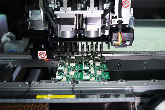
Next, printing solder paste and preparing components, then place them onto the PCB board according to the BOM file (bill of material). After setting up the pick and place machine, automated machines can precisely position each component based on the design.

Soldering

The components are soldered to the PCB. This can be done using methods like wave soldering or reflow soldering to ensure everything is securely attached and electrically connected. You must know, different products require different parameters, please make sure all the parameters like temperatures, time are suitable.

Inspection and Testing

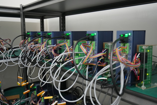
The assembled CCA goes through rigorous inspection and testing to ensure it works as intended. This includes visual inspections, automated optical inspections (AOI), in-circuit testing (ICT), aging testing and functional testing.

Final Assembly

If the CCA passes all tests, it moves on to final assembly, where it’s integrated into the larger electronic system or device. That is we say the box building assembly.

What are the types of circuit card assembly?

CCAs can be divided into various types according to the different manufacturing technology.

Through-Hole Technology (THT) Assembly

Here, components have leads or pins inserted into holes drilled through the PCB and soldered on the other side. This method provides strong mechanical bonds, making it great for components that experience mechanical stress. It’s often used in aerospace, military, and industrial equipment.

Surface Mount Technology (SMT) Assembly

In SMT, components are mounted directly onto the PCB surface using solder paste. No drilling required, which allows for higher component density and smaller PCBs. This method is commonly used in consumer electronics, telecommunications, and automotive industries.

Box Building Assembly

Box building assembly involves the complete assembly of electronic systems, including CCAs, into enclosures or boxes. This process includes not only the assembly of the PCB but also the integration of cables, connectors, and other components into a final product. Box building is ideal for producing complete electronic devices ready for end-use.

Advanced materials for CCAs

Advanced materials help CCAs perform better and last longer:

  • High-Temperature Laminates (e.g., FR-4, Polyimide)

High temperature laminate like FR4 or polyimide. These materials can handle extreme conditions without breaking down. FR-4 is popular for its excellent thermal and mechanical properties, while polyimide is great for high-temperature stability.

  • Flexible Substrates (e.g., Kapton, PET)

Kapton and PET are the most common flexible substrate. These materials allow CCAs to bend and flex. Kapton, a type of polyimide, is known for its high thermal resistance and flexibility, making it perfect for wearable electronics and medical devices. PET (polyethylene terephthalate) is another flexible material with good electrical insulation properties.

  • Advanced Solder Compounds

SAC305 (a lead-free alloy of tin, silver, and copper) is favored for its mechanical and thermal properties. Whatever you want to mount a ceramic PCB or the flexible PCB, it is the best choice. Sn63Pb37, a traditional tin-lead solder, is still used for its ease of use and excellent performance.

Reliable circuit card assembly manufacturers

Choosing the right manufacturer for your CCAs is key to getting quality products. PCBonline and EBest Circuit (Best Technology) are go-to-choice reliable circuit card assembly manufacturers. Both of them has advanced pick and place machine, full-auto SPI, AOI equipment, ensuring a good quality.

As a leading manufacturer in the circuit card assembly, EBest Circuit (Best Technology) prides full turn-key service, ranging from the PCB design, PCB fabricating, electronic component sourcing, circuit card assembly and box build assembly. We handle complex and high-volume orders efficiently, ensuring timely and fast delivery without sacrificing quality. In 2023 alone, we completed over 5000 high-complexity projects with a client satisfaction rate of over 98%.

It is crucial for anyone to fullly understand the circuit card assembly in the electronics industry. From their basic components and manufacturing process to the advanced materials used, CCAs are the backbone of modern electronic devices.

You may also like

PWB Vs. PCB: What Are the Manufacturing Process Differences?
Thursday, July 4th, 2024

In our daily life, electronic devices are existing everywhere. And there are many people know the “PCB” nowadays, while very less people know the “PWB”. Unless you’ve been in the PCB business for more than 20 years.

Actually, PWB is another term of circuit board, and it was used commonly before the year 1999. But with the development of electronics, it was replaced by PCB gradually. You want to know more about it? In this article, we will answer it for you. Deeply explain their definitions, manufacturing process, applications and the key differences between PCB and PWB.

PWB Vs. PCB: What Are the Manufacturing Process Differences?

What is A Printed Circuit Board (PCB)?

A Printed Circuit Board is a fundamental component in modern electronics, providing the physical and electrical connections for various electronic components. It consists of multiple compositions, including a non-conductive substrate, conductive pathways, and insulating layers, which facilitate the complex circuitry required in contemporary devices. A PCB can be made into single sided PCB, double sided PCB and multilayer PCB.

PCBs are integral to the functionality of a wide range of electronic products, from consumer gadgets like smartphones and computers to industrial machinery, medical devices, and aerospace systems. The advanced design and manufacturing processes involved in PCB production ensure high reliability and performance, making them essential in virtually all electronic applications.

PWB Vs. PCB: What Are the Manufacturing Process Differences?

Basic manufacturing process of PCB

Design and Layout

PCBs are designed using sophisticated computer-aided design (CAD) software. Designers create detailed layouts, specifying the placement of components, conductive pathways, and vias (interlayer connections). The design is converted into Gerber files, a standard format for PCB fabrication that contains all the necessary information for manufacturing. These files are essential for ensuring precision and accuracy during the manufacturing process.

Material Preparation

The substrate, typically FR4 (fiberglass epoxy laminate), is prepared. FR4 is known for its excellent mechanical strength and thermal stability, making it an ideal base material for PCBs. Copper sheets are laminated onto the substrate, which will form the conductive pathways after the etching process. This preparation stage is crucial for creating a reliable foundation for the PCB.

Printing the Circuit Pattern

A photoresist, a light-sensitive material, is applied to the copper-clad substrate. The board is exposed to ultraviolet (UV) light through a mask that defines the circuit pattern. The UV light hardens the photoresist in the exposed areas. The board is then developed in a chemical solution that removes the unexposed photoresist, revealing the copper to be etched away. This step accurately transfers the circuit design onto the board.

Etching

The board is immersed in an etching solution, commonly ferric chloride or ammonium persulfate, which removes the unprotected copper, leaving only the desired circuit pattern. This etching process is crucial for defining the conductive pathways on the PCB, ensuring that the correct connections are made according to the design specifications.

Drilling

Precision drilling machines are used to create holes for through-hole components and vias. These holes are then cleaned to remove any debris that could affect electrical connectivity. Drilling is a critical step in the PCB manufacturing process as it ensures proper placement and connection of components across different layers of the board.

Plating

The drilled holes are plated with copper to create electrical connections between the layers, which is especially important for multilayer PCBs. Additional layers of plating, such as nickel or gold, may be applied to improve conductivity and protect against oxidation. This plating process enhances the durability and performance of the PCB.

Solder Mask Applying

A solder mask is applied to protect the copper traces from oxidation and prevent solder bridges between closely spaced solder pads. The solder mask is exposed to UV light and then developed to reveal the solder pads. This layer not only protects the PCB but also improves its appearance and reliability.

Silkscreen Printing

A silkscreen layer is printed on the board to add text, component labels, and other identifiers. This layer helps in the identification and assembly of components, making it easier for technicians to work with the PCB during the manufacturing and repair processes.

Surface Finishing

Generally, a layer of surface finishing is coated on the PCB to protect its surface, it also called surface treatment. The common surface treatments are HASL-LF, ENIG, ENEPIG, OSP, Immersion Silver/Tin. Of course, different treatment offers different function, like OSP is to protect surface from oxidation, HASL-LF provides a good solderability, ENEPIG make sure the chemistry corrosion. Choose a suitable one according to your specific demands.

Assembly and Testing

Components are placed on the board using automated pick-and-place machines, and soldered using techniques like reflow soldering for surface-mount devices (SMD) and wave soldering for through-hole components. The finished PCB undergoes various tests, such as automated optical inspection (AOI), electrical testing, and functional testing, to ensure quality and performance. Want see the whole manufacturing process of a multilayer PCB, click here: Manufacturing Process of Multi-layer PCB.

PWB Vs. PCB: What Are the Manufacturing Process Differences?

What is the definition of Printed Wiring Board (PWB)?

A Printed Wiring Board is a term historically used to describe a type of circuit board that focuses primarily on the layout and wiring of electronic connections rather than the overall circuit functionality. PWBs emphasize the physical arrangement of conductive paths to connect various components but do not necessarily include all the integrated features found in modern PCBs.

PWB Vs. PCB: What Are the Manufacturing Process Differences?

This term was more prevalent during the earlier stages of electronic development, where the primary concern was establishing reliable electrical connections. As technology advanced, the term PCB became more common, reflecting the expanded capabilities and comprehensive role of these boards in forming complete electronic circuits. Despite being less common today, understanding the term PWB is crucial for historical context and certain niche applications.

How to Manufacture A Printed Wiring Board (PWB)?

Design and Layout

PWBs typically have simpler designs focused on wiring patterns rather than complex circuitry. In some cases, the layout may be done manually or using basic design software.

Material Preparation

Simpler substrates such as phenolic or epoxy resins may be used for PWBs. Copper sheets are laminated onto the substrate to form the conductive pathways. These materials are cost-effective and suitable for applications where advanced performance characteristics are not required.

Printing the Wiring Pattern

Similar to PCBs, a photoresist is applied to the copper-clad substrate. The board is then exposed to UV light through a mask and developed to reveal the copper to be etched away. This process creates the wiring pattern necessary for connecting electronic components.

Etching

The board is immersed in an etching solution to create the wiring pattern. This step is straightforward compared to the more intricate etching processes used in PCB manufacturing, reflecting the simpler requirements of PWBs.

Drilling

Holes for through-hole components are drilled, but the process may not require the precision needed for complex PCBs. This basic drilling process is adequate for the less demanding applications of PWBs.

Plating (if necessary)

Plating is done to ensure electrical connectivity but may not involve advanced techniques like those used for multilayer PCBs. It suffices for the simpler construction of PWBs.

Solder Mask Application

A basic solder mask may be applied to protect the wiring pattern. This layer provides sufficient protection for the relatively simple designs of PWBs, preventing short circuits and oxidation.

Silkscreen Printing

A simple silkscreen layer may be added for component identification. This helps in the assembly process but does not require the detailed labeling often necessary for PCBs.

Assembly and Testing

Components are manually or semi-automatically placed on PWBs and soldered using standard techniques. Basic electrical testing is conducted to ensure functionality. This simpler assembly and testing process aligns with the less complex nature of PWBs.

pcb assembly

Which Kind of Materials used in PCB and PWB?

Substrate Materials

FR4 (fiberglass epoxy laminate) is the most common substrate material for PCBs due to its excellent mechanical strength and thermal stability. Phenolic resin, used in PWBs for simpler applications, is less durable and has lower thermal stability compared to FR4, but it is cost-effective and suitable for basic electronic devices. Polyimide is used for flexible PCBs due to its high flexibility and thermal resistance, making it ideal for applications requiring bending and flexing, such as wearable electronics and flexible displays.

Conductive Materials

Copper is the primary conductive material for both PCBs and PWBs. It is used to create the conductive pathways and pads, providing excellent electrical conductivity and reliability. Gold, nickel, and silver are used for plating to enhance conductivity and protect against oxidation, primarily in PCBs. These materials improve the durability and performance of the PCB by providing a reliable contact surface for soldering and component connections.

Insulating Materials

Prepreg, a fiberglass cloth impregnated with resin, is used in multilayer PCBs to bond the layers together. Prepreg provides mechanical strength and electrical insulation between the layers. Dielectric materials are used between layers in multilayer PCBs to provide electrical insulation, maintaining signal integrity and preventing short circuits.

Solder Mask Materials

Liquid Photo Imageable (LPI) solder mask is the most common type used in PCBs, providing excellent protection and durability. LPI solder masks are applied using a photolithographic process, ensuring precise coverage and protection. Dry film solder mask is used for simpler applications and PWBs. This type of solder mask is less expensive and easier to apply but may not offer the same level of protection as LPI solder masks.

Key differences between PCB and PWB

FeaturePCB (Printed Circuit Board)PWB (Printed Wiring Board)
Design and LayoutDesigned using sophisticated CAD tools for complex circuitry, including detailed simulation and optimization.Simpler designs focused on wiring patterns, often done manually or with basic software.
Layer CountCan have multiple layers (e.g., double-sided, multilayer) to support intricate circuit designs.Generally single or double-sided, less commonly multilayer.
Component TypesSupports surface-mount technology (SMT) and through-hole technology (THT) components.Primarily supports through-hole technology (THT) components.
Signal IntegrityDesigned to maintain high signal integrity, minimizing electrical noise and interference.Basic signal integrity management, sufficient for simple applications.
Flexibility and RigidityIncludes both rigid and flexible PCBs, allowing for a wide range of applications.Typically rigid, not commonly used in flexible applications.
Terminology and UsageUniversally used in the industry to refer to boards that integrate all necessary components to form complete circuits. Also called “bare board”.Universally used in the industry to refer to boards that integrate all necessary components to form complete circuits.
Industry StandardsRecognized by standards organizations like IPC, IEC, and ANSI with specific performance and quality criteria.Covered under broader standards but with fewer specific guidelines due to limited modern use.
Cost and EfficiencyHigher cost due to advanced materials and processes, offering superior performance and reliability.More cost-effective for simple applications, but with limited performance and reliability.
ApplicationsUsed in consumer electronics, industrial equipment, medical devices, aerospace, and defense.Historically used in simpler electronic devices and early computers, still relevant in niche applications.
(Summary Differences: PCB VS PWB)

Other Terms Related to PWB and PCB

Based on the PCB and PWB, you may still hear about CCA, PCA, PWA during the PCB working. These terms are also related to printed circuit board. Here is a detailed explanation of each:

Printed Wiring Assembly (PWA)

PWA is the abbreviation for printed wiring assembly. This is an archaic term that was once used to describe what we now refer to as PCB assembly or PCBA. Although it is less common today, understanding this term is useful for historical context and when dealing with older documentation.

Circuit Card Assembly (CCA)

CCA stands for circuit card assembly. It is essentially the same thing as PCBA, where the PCB is assembled with all necessary components to create a functional unit. CCA is a less frequently used term compared to PCBA but is still recognized in certain industries and contexts.

Printed Circuit Board Assembly (PCBA)

PCBA is the abbreviation for printed circuit board assembly. When the PCB is assembled with all its electronic components by SMT technology, it is called PCBA or PCB assembly. Since a change in terminology in 1999, PCBA has become the standard term used for all assembled circuit boards. From users to technical committees, PCBA is the preferred term for referring to assembled boards. The assembly process involves placing and soldering components onto the PCB, making it a functional electronic circuit.

Printed Circuit Assembly (PCA)

PCA stands for printed circuit assembly, which is another term for PCBA. Like CCA, PCA is not commonly used in modern terminology but refers to the same concept of an assembled printed circuit board.

aging test of PWB boards

In a word, whatever for PWB, PCB, or circuit cards, they are refer to bare printed circuit boards (bare boards). While PCA, CCA, PWA, and PCBA refer to assembled circuit boards. Among these terms, PCB and PCBA are the most widely used in both industry and technical documentation.

This is the end of this introduction of PWB and PCB, welcome to contact us if you want more about PCB knowledge.

You may also like

What Are the Differences Between Active and Passive Components?
Wednesday, July 3rd, 2024

In PCB electronics, components are classified into two main categories: active and passive components. Understanding these differences is crucial for anyone working with electronic circuits. Active components control electricity flow and require an external power source. Passive components do not control electricity and do not need an external power source.

What are active and passive components meaning?

Active and passive components, simply say, the device that needs an energy (electrical) source is called an active device, and the device that does not need an energy source is a passive device. Active components, such as transistors and diodes, require external power to function. They can control the flow of electricity. Passive components, like resistors and capacitors, do not need external power. They cannot control electrical flow but can store, resist, or filter energy. Both passive and active components are common useful in PCB assembly and SMT technology.

Active components play a dynamic role in circuits. They can amplify signals, switch currents, and perform various complex functions. These components rely on an external power source to operate and influence the behavior of the circuit. For instance, a transistor can amplify a weak signal, making it stronger and more useful for further processing.

What Are the Differences Between Active and Passive Components?

Passive components, on the other hand, are more static in nature. They cannot amplify signals or control current flow but are essential for other functions like energy storage and signal filtering. Resistors, capacitors, inductors, and transformers are common examples. Each of these components has a specific role in maintaining the stability and functionality of an electronic circuit.

What are the key differences between active and passive components?

The main difference between active and passive components is their ability to control electricity. Active components can amplify signals and perform complex tasks. Passive components can only store, resist, or filter energy. They cannot amplify signals or control current.

Active components are energy-dependent. They require an external source of power to function and can influence the flow of electricity within the circuit. For example, an integrated circuit (IC) can perform multiple functions like amplification, switching, and signal modulation, all of which require external power.

Passive components, in contrast, do not require an external power source. They can only perform their functions passively. For instance, a resistor can limit the current flowing through a circuit without needing additional power. Similarly, a capacitor can store electrical energy and release it when needed, all without external energy input.

Common active components in electronics

Active devices are the main components of electronic circuits. From the physical structure, circuit function and engineering parameters, active devices can be divided into discrete devices and integrated circuits.

1. Discrete devices

  • Bipolar transistor, generally referred to as transistor or BJT
  • Field effective transistor
  • Thyristor
  • Semiconductor resistors and capacitors – resistors and capacitors manufactured by integrated technology are used in integrated circuits.

2. Integrated circuit

Integrated circuit can be divided into analog IC and digital IC. Analog integrated circuits mainly deal with continuous analog signals, such as sound, light, temperature, etc., and retain the continuity and accuracy of the signal through amplification, filtering, mixing and other operations. In contrast, digital integrated circuits are used to process discrete time digital signals, convert the signal into binary digital form, and then perform logical operations and processing.

Basic analog integrated circuit devices generally include:

  • Integrated operational amplifier (operation amplifier)
  • Comparator
  • Logarithmic and exponential amplifiers
  • Multiplier/divider
  • Analog switching circuit (analog switch)
  • Phase lock loop
  • Integrated voltage regulator
  • Reference source
  • Wave-form generator
  • Power amplifier

Digital integrated circuit including:

  • Logic gate circuit
  • Flip-flop
  • Register
  • Decoder
  • Data comparator
  • Driver
  • Counter
  • Shaping circuit
  • Programmable Logic Device (PLD)
  • Microprocessor (MPU)
  • Microcontroller (MCU)
  • Digital signal processor (DSP)

Common passive components in electronics

Passive devices in electronic systems can be divided into circuit components and connection components according to the circuit functions they play. These components are essential for functions like energy storage, filtering, and impedance matching in electronic circuits. The common passive components are including:

Circuit components

  1. Diode
  2. Resistor
  3. Resistor network
  4. Capacitor
  5. Inductor
  6. Transformer
  7. Relay
  8. Key
  9. Speaker
  10. Switch

Connection components

  • Connector
  • Socket
  • Cable
  • PCB (printed circuit board)

Why are active components crucial in modern electronics?

The ability of active components to control and manipulate electrical signals makes them indispensable in a wide range of applications.

In computers, for example, active components such as processors and memory chips perform complex calculations and store large amounts of data. In communication systems, active components amplify weak signals, making long-distance transmission possible. Without these amplifiers, the signal would decay with distance, leading to a decline in communication quality. Power electronics, another key area of modern development, relies heavily on active components. Devices like power converters, inverters, and motor controllers use transistors and integrated circuits to efficiently convert and control electrical energy. This efficiency is crucial for applications ranging from renewable energy systems to electric vehicles.

It’s fair to say that without active components, devices like computers, smartphones, and TVS wouldn’t function the way they do today, and our era of big data wouldn’t be moving as fast as it is today.

How do passive components complement active components?

Both active and passive components are indispensable in a circuit. They depend on each other and complement each other. Without active components, the circuit cannot be activated or perform a specific work. Without passive components, the circuit cannot be controlled and adjusted, nor can it achieve a stable operating state. Such a relationship between the two is like the relationship between the “dynamic” and the “static” of a circuit.

What Are the Differences Between Active and Passive Components?

For example, in an audio amplifier circuit, the power supply and amplifier are the active components, and the load and resistance are the passive components. The power supply provides energy, the amplifier amplifies the signal, and controls and limits it through load and resistance, and finally realizes the amplification and regulation of the audio signal. In signal processing, inductors filter out high-frequency noise and protect sensitive active components from interference. Transformers, on the other hand, enable efficient power transfer between different parts of the circuit, allowing active components to operate within their optimal voltage range.

Comparing the Energy Requirements of Active and Passive Elements

Active components need an external power source to function. They consume energy during operation. Passive components do not need external power and generally do not consume energy, except for minor resistive losses. This difference impacts the design and efficiency of electronic circuits.

Active components, such as transistors and integrated circuits, rely on external power to operate. This power requirement means that active components consume energy during their operation. The amount of energy consumed depends on the specific component and its application. For instance, a power amplifier consumes more energy than a simple transistor switch.

Passive components, in contrast, do not need external power to function. They operate solely based on the electrical energy present in the circuit. Resistors, capacitors, and inductors do not consume significant energy, except for minor resistive losses in resistors. This low energy requirement makes passive components more efficient in certain applications.

What Are the Differences Between Active and Passive Components?

The difference in energy requirements between active and passive components impacts the overall efficiency of electronic circuits. Designers must carefully balance the use of active and passive components to achieve optimal performance and energy efficiency. For example, using passive filters instead of active ones can save energy in low-power applications.

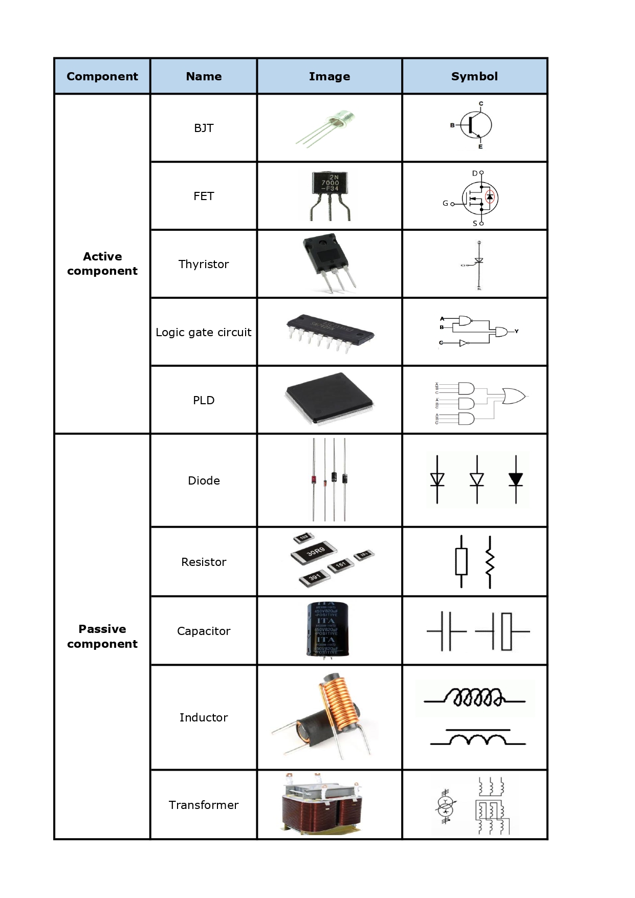
Active and Passive Component Images and Symbols

Recognizing symbols are essential for reading and designing circuit diagrams. They provide a visual representation of the components and their functions, helping designers understand the overall structure and operation of the circuit. Recognizing these symbols is a fundamental skill for anyone involved in electronics. Here is a detailed images and symbols listing of common active and passive components.

Above all is the introduction to passive and active components, hope it is useful for every engineers. EBest Circuit (Best Technology) is a professional PCB and PCBA manufacturer in Asia. We have our own factory in China and Vetnam. Welcome to contact us if you have any questions about components and PCB assembly.

You may also like

X-ray Inspection in PCB Assembly
Wednesday, June 15th, 2022

X-Ray Inspection’s Definition

X-ray inspection is a technology used to inspect the hidden features of the target objects or products. As for PCB inspection, X-ray is commonly used in the inspection of PCB assembly in order to test the quality and find the hidden defects, X-ray inspection is one of the most important steps for quality-oriented PCB manufacturers.

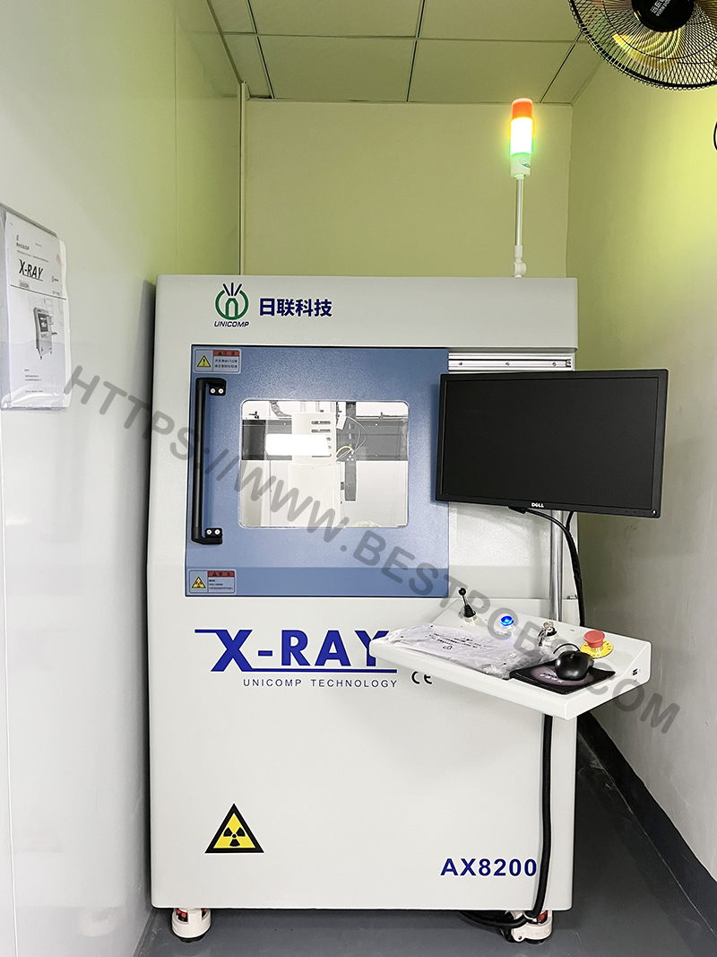
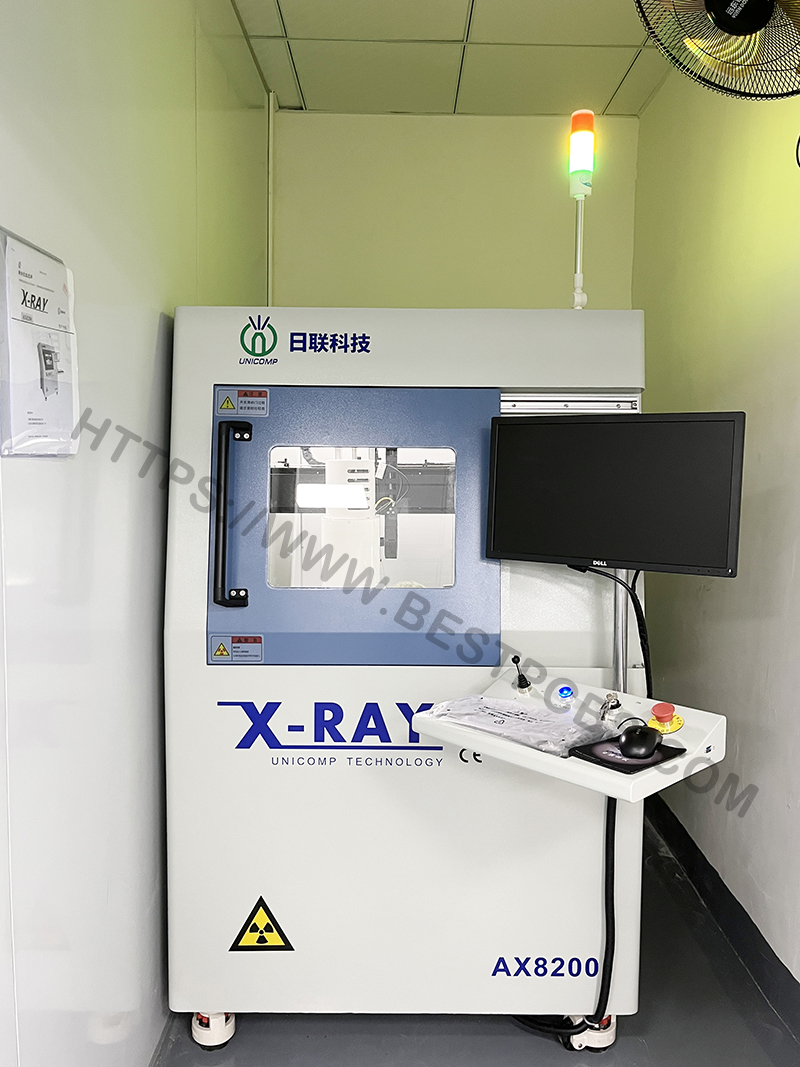
X-Ray Machine

X-Ray Inspection’s Working Principle

Generally, there are three elements in the X-ray devices.

  • X-ray tube—to generate the X-ray photons.
  • Operation platform—to move along with the sample so that the sample can be inspected from different angles and magnification.
  • Detector—it can capture the X-ray through the samples and then transfer it into the image so that we can find out whether there are defects on the printed circuit board.

The Hidden Defects that can be Identified by X-Ray

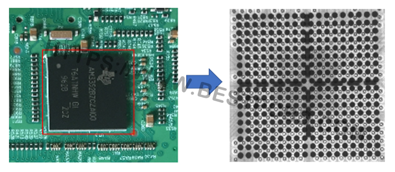
Since PCB has the higher density with the solder joints hidden and holes buried or blind, X-ray enable us to inspect the quality of the PCB and identify various hidden defects. And there are three common hidden defects that can be inspected by X-ray.

PCB’s Image Under X-Ray
  • Solder bridges—it is a common issue that will occur when the solder joints are so close that they create a connection which is not allowed. And usually, the solder bridges will be covered by some components on the PCB. But they can be easily found with the help of the X-ray device.
  • Solder voids—when gas or flux is entrained during welding, solder voids will be produced, which will lower the thermal conductivity at the solder joint and may cause physical defects. And X-ray can help to  identify the solder voids
  • Pin-hole fills—pin-hole fills issue is a common problem occurring in the plug-in components on the  printed circuit boards. The X-ray device can be used to identify these errors, and can even quantify the missing filling amount.

Our X-Ray Inspection Device

The maximum size of the board that can be put in the device’s operation platform is 510*430 mm, while the maximum inspection size of the device is 435*385 mm. So here is the manifestation of the operation platform’s function. When the size of PCB is over 435*385 mm, the operation platform will move along with the board so that the board can be inspected thoroughly.

And here is a video about operation of our X-ray inspection device.

So, this is the end of this article. In case if you have any questions, you are welcome to contact us via email at  sales@bestpcbs.com. We are fully equipped to handle your PCB  manufacturing requirements.

You may also like

Types of Vias
Friday, May 20th, 2022

What is via?

A via plays an important role in multi-layer PCBs. It is used to make an electrical connection between the layers of a multi-layer PCB. Generally speaking, every hole in the printed circuit boards can be called as via.

A via is constructed by placing copper pads on each layer of the PCB and drilling a hole through them. And the hole is plated with copper that forms electrical connection through the insulation that separates the copper layers.

PCB Vias

Types of Vias

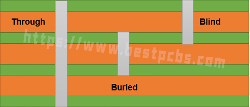
There are three main types of vias used in PCB: through-hole via, blind via and buried via.

Through-Hole Via

Through-hole via goes right through the printed circuit board from top to bottom and can be used to connect all the layers of a PCB. It is the most common via and is easiest to construct.

Blind Via

Blind via connects the outermost layer of a PCB to the next layer. Namely, it cannot be seen on the other side of the board and is therefore called blind via.

Buried Via

Buried via is used to connect internal layers of a PCB. And it cannot be seen on the surface of the board.

Via Types

In addition, it is always better to use multiple smaller vias rather than one large via since smaller vias can reduce the inductance and also provide an additional path to the current flow in case any of the vias fail.

So, this is the end of this article. In case if you have any questions, you are welcome to contact us via email at  sales@bestpcbs.com. We are fully equipped to handle your PCB  manufacturing requirements.

You may also like

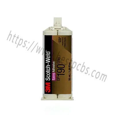
3M Epoxy Adhesive DP190-Gray & 3M Epoxy Adhesive DP190-Translucent
Friday, April 22nd, 2022

Both 3M Epoxy Adhesive DP190-Gray and 3M Epoxy Adhesive DP190-Translucent are a two-part epoxy adhesive that delivers exceptional performance with high shear and peel strength.

They can bond to a wide range of materials, such as metals, ceramics, wood, fiberboard, glass, rubber and many plastics. So, PCB is no exception. But what are the similarities and differences between them?

Similarities

  • Provide tough, strong bonds through high shear and peel strength.
  • Capable of bonding to a wide variety of different materials.
  • Deliver extended work-life, providing additional time for adjustment.
  • Exhibit good environmental aging properties, delivering long-term durability.

Differences

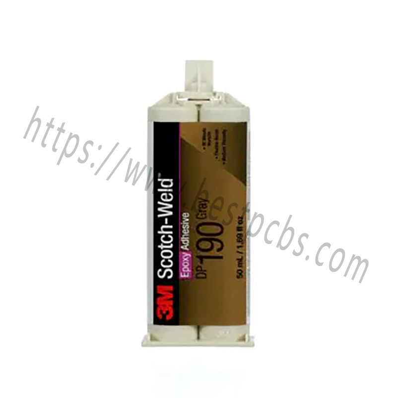
3M Epoxy Adhesive DP190-Gray has a moderately high modulus. With a 90-minute work-life, it reaches handling strength in approximately 10 hours and full cure in 7 days at room temperature.

Additionally, this epoxy adhesive has medium viscosity and self-leveling with a 1:1 mix ratio by volume. But its flexibility and elongation are moderate.

(3M Epoxy Adhesive DP190-Gray)

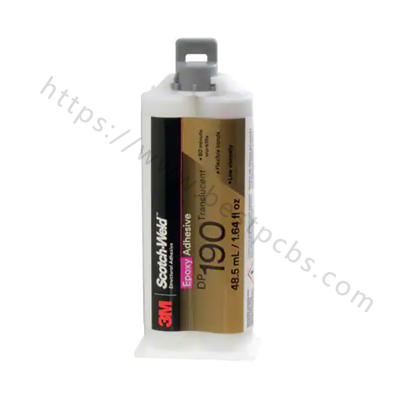
3M Epoxy Adhesive DP190-Translucent has a moderately low modulus. With an 80-minute work-life, it reaches handling strength in approximately 10 hours and full cure in 14 days at room temperature.

It has low viscosity and self-leveling with a 1:1 mix ratio by volume. Additionally, it features high flexibility and elongation.

3M Epoxy Adhesive DP190–Translucent

This is all about the similarities and differences between the 3M Epoxy Adhesive DP190-Gray and 3M Epoxy Adhesive DP190-Translucent. It is supposed that you have known about them.

But if you still have any questions about them or PCB, please feel free to contact us. Because at EBest Circuit (Best Technology), we are fully equipped to handle your PCB manufacturing requirements.

You may also like

Can you tell the difference between PWB and PCB?
Wednesday, May 20th, 2020

The abbreviations PWB and PCB are very common, especially in the field of electronics manufacturing. Therefore it is necessary to gain a clear understanding of the meaning of each one and the differences between the two. On this article, we will help our readers to distinguish PWB from PCB.

pcb vs pwb
pcb vs pwb

PCB: Based on insulating substrate, it means a kind of products on which the wires are connected and components are printed from point to point on a dielectric substrate in a predetermined design. It is the English abbreviation of Printed Circuit Board.In a word, PCB stands for printed circuit board, where the width, side to side and multi-layer relationship(spacing) of conductor runs has or is designed to have a specific effect on circuit operation other than just a point to point connection.

PWB: Based on insulating substrate, it means a kind of products on which the wires are connected from point to point on a dielectric substrate in a predetermined design. However, there is no printed component on it. PWBs are the early name of the British, because at that time there were only circuit diagrams on the circuit board, but no printed components. So they belonged to the more primitive board. Under its effect, now many traditional British and some Hong Kong people still call the circuit board to be PWB, which is the English abbreviation of Printed Wire Board. In a word, PWB stands for printed wiring board, one of the first uses when the issue was only a point to point connection.

The PCBs are the boards already equipped with various components, however the PWB is just a designed substrate with no components.

pcb vs pwb
pcb vs pwb

Moreover, PWB vs PCB greatly varies from one region to the other. For example, in the United States of America, the term Printed Circuit Board is more common in use while the use of the name PWB is more commonly used in Japan. In Japan, PWB is more preferred that PCB because it prevents confusion with another name, polychlorinated biphenyls, which refers to a particular poison available in Japan.

For your more information, in approximately 1999 the IPC Technical Activities Executive Committee made a mandate to only use the term PCB for all new document development because more often than not the printed circuitry design will have an impact on function.

If you are still confused or have any queries or comments about PCB, do not hesitate to contact us. Our sales team can give you a reply at our soonest convenience.

You may also like