PCB manufacturing PCB manufacturing
Home > Blog

pcb design

Unlock the Full Power of Circuit Board White
Tuesday, February 11th, 2025

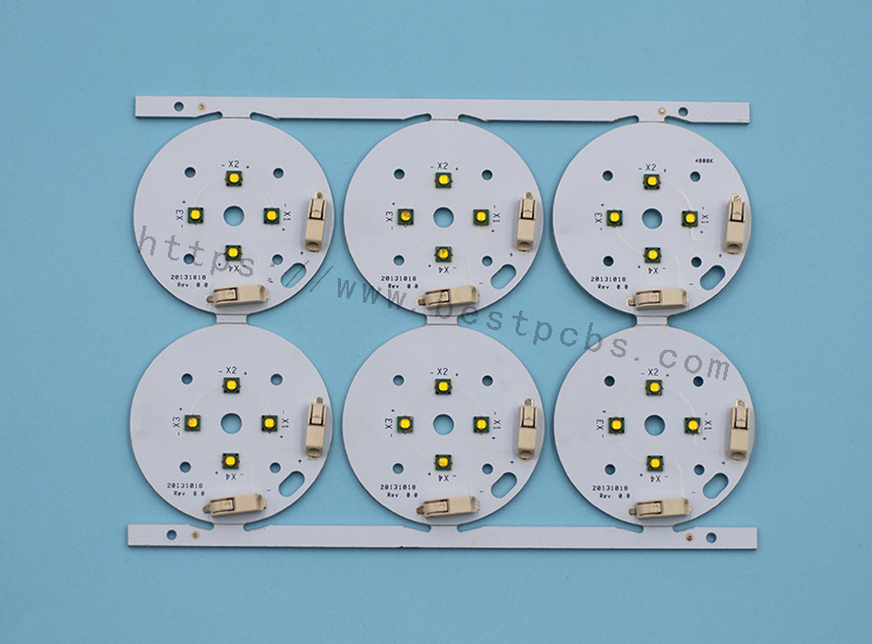
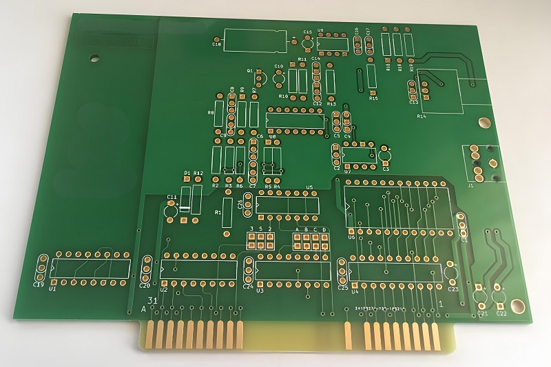
Circuit board white is more than just an aesthetic trend. It’s quickly becoming a common choice in PCB (Printed Circuit Board) design, thanks to its sleek look and unique benefits. When compared to traditional PCBs, white circuit boards offer enhanced performance and a polished finish that suits many modern applications. In this article, we’ll explore what makes circuit board white stand out, the advantages it offers, and why it’s gaining popularity in various industries.

What Is Circuit Board White?

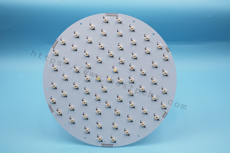
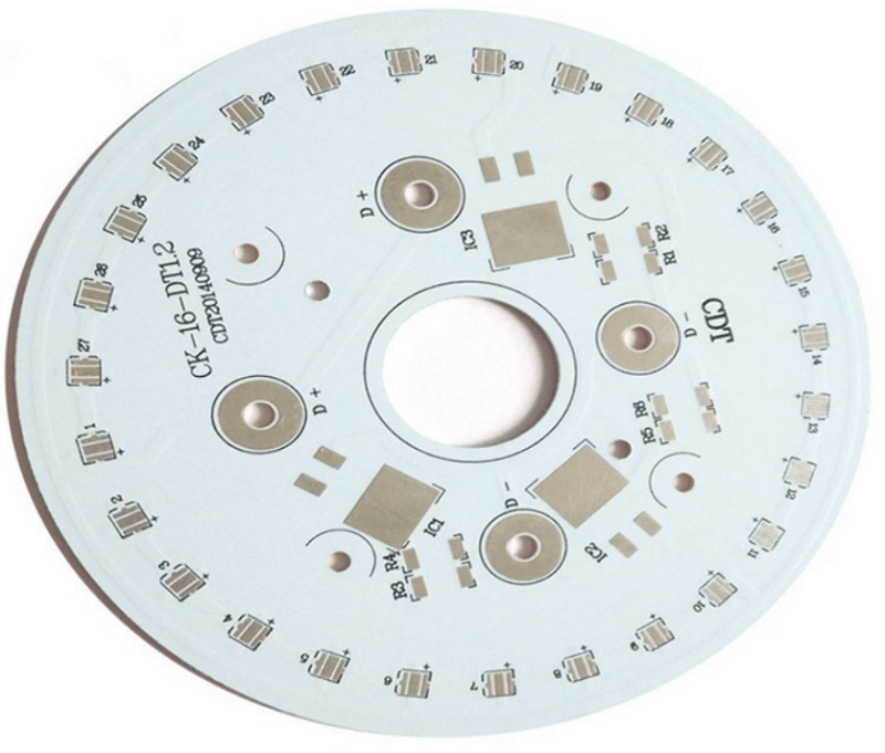
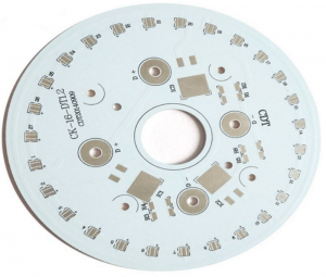
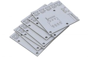
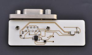
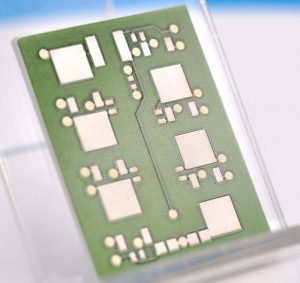
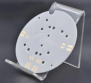
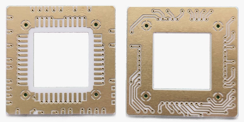
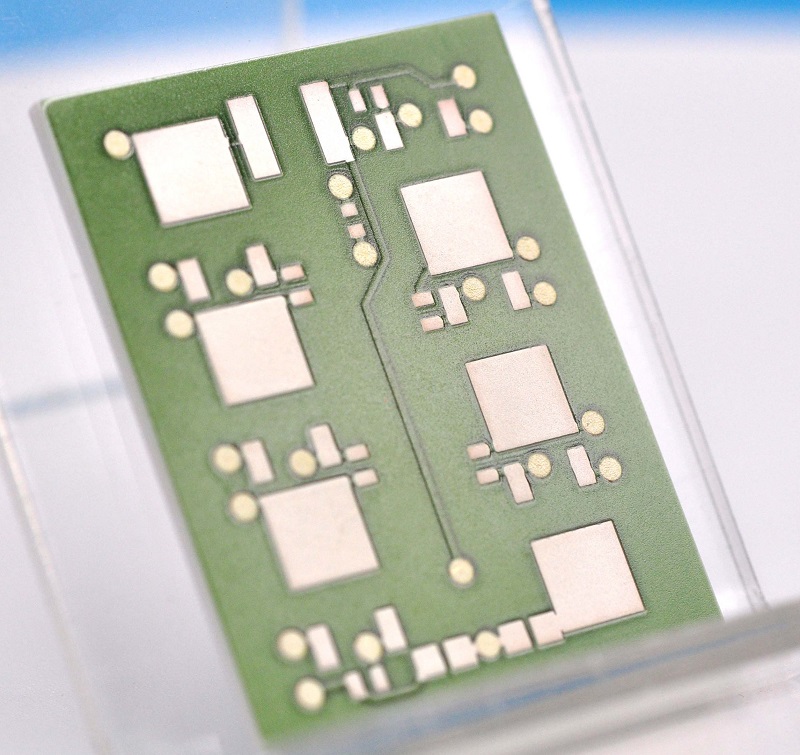
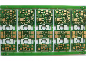
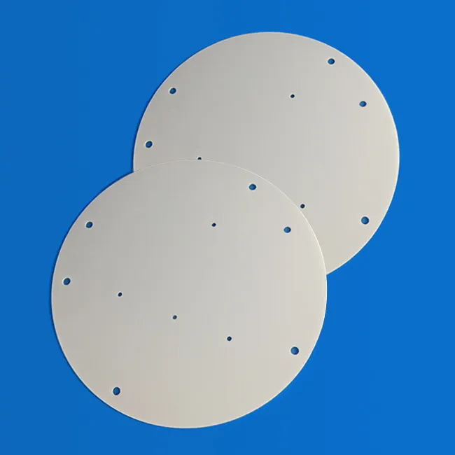
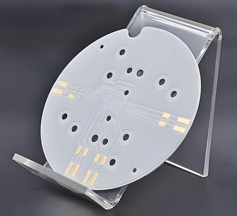
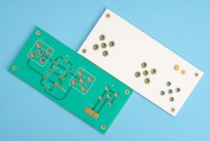
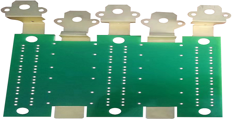
Circuit board white refers to PCBs that are produced with a white surface finish, rather than the typical green, black, or other colored finishes seen in standard PCBs. This white finish is achieved using specific materials and coatings that provide an eye-catching, clean look while still maintaining the reliability and performance that is expected from PCBs.

The choice of white as a color for PCBs may initially seem purely aesthetic, but it serves several functional purposes as well. It enhances the visual appeal of the circuit board, making it suitable for applications where appearance matters. But more importantly, the white surface helps in better heat dissipation, which is a critical factor in PCB design for high-performance electronics.

White PCB vs. Standard PCBs: What’s the Difference?

When comparing white PCBs to standard ones, the most obvious difference is the color, but there’s more to it than that. White PCBs are often constructed using materials that offer better heat management, which can improve the overall performance and lifespan of the device. Additionally, the reflective surface of a white PCB can provide better visibility for inspections, making the production process smoother.

On the other hand, traditional PCBs typically use green or black colors, which are cost-effective and effective in their own right. However, white PCBs may be preferred for high-end consumer electronics or products that require a more polished, professional appearance. They also often have a slight advantage in terms of thermal performance, as the white surface helps reflect heat away from the components.

In short, while traditional PCBs are still the go-to for most industries, white PCBs are emerging as the better option for those who need both form and function in their designs.

How White Printed Circuit Boards Improve Heat Dissipation?

Heat dissipation is one of the most critical factors in PCB design. Overheating can lead to performance issues and even failure of electronic devices. White printed circuit boards are known for their ability to dissipate heat more effectively than their darker counterparts. This is due to the reflective nature of the white surface.

The reflective properties help scatter heat away from the PCB, reducing the temperature buildup around sensitive components. This is especially useful in high-power applications like automotive systems, medical devices, and even some consumer electronics, where overheating could cause significant damage or degradation in performance.

By improving heat dissipation, white PCBs not only extend the life of the device but also enhance its reliability, making it a smart choice for demanding applications.

What Is the Manufacturing Process Behind White Printed Circuit Boards?

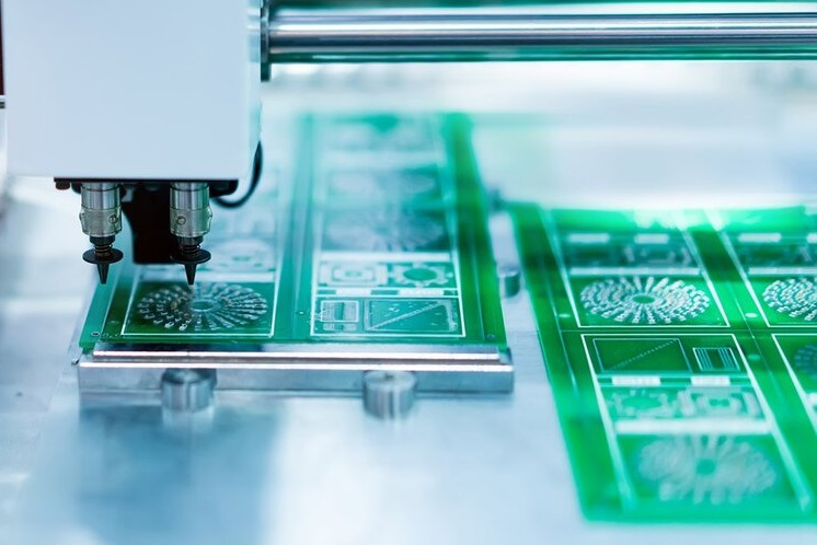
The manufacturing process for white printed circuit boards is similar to traditional PCBs, with a few key differences. First, manufacturers use specialized white coating materials that give the circuit board its bright appearance. These coatings are applied during the lamination process, where layers of copper, resin, and other materials are bonded together.

The process also involves precision etching to create the circuit pathways, just like in traditional PCBs. However, the final touch is the white coating, which is often baked onto the PCB to ensure it adheres properly and maintains its durability over time.

Due to the nature of the white finish, manufacturers have to pay extra attention to quality control during production. This ensures that the white surface remains smooth and uniform, contributing to both the aesthetic appeal and functionality of the PCB.

Are White PCBs More Durable Than Traditional Circuit Boards?

In general, the durability of a PCB depends on the materials used and the manufacturing process rather than the color. However, white PCBs tend to be slightly more durable when it comes to their surface integrity. The white coating used on these boards is typically designed to withstand harsh environments, making them resistant to scratches and other physical damage.

In addition to their surface resilience, the heat dissipation properties of white PCBs also contribute to their overall durability. By keeping the temperature within optimal levels, white PCBs help prevent the components from overheating, which could otherwise lead to premature wear and tear.

Overall, while the color itself doesn’t directly impact the PCB’s durability, the advanced materials and coatings used in white PCBs often offer a slight edge in terms of longevity and resistance to damage.

Which Top Industries Use White Circuit Boards in Their Products?

White circuit boards are increasingly finding their way into various industries due to their functional and aesthetic benefits. Some of the top sectors utilizing white PCBs include:

Consumer Electronics: White PCBs are commonly used in smartphones, wearables, and high-end home appliances due to their clean, modern look.

Medical Devices: In medical technology, where both aesthetics and performance matter, white PCBs help maintain device integrity while offering easy inspection.

Automotive Industry: White PCBs help manage heat dissipation in electric vehicles, which require reliable and efficient electronics.

Aerospace: The aerospace industry benefits from the lightweight and heat-reflective qualities of white PCBs, ensuring high performance under extreme conditions.

As demand for high-performance, visually appealing products grows, the use of white PCBs will continue to spread across these and other industries.

How to Customize White PCBs for Your Unique Needs?

One of the major advantages of white PCBs is the ability to customize them for specific requirements. Customization options include varying the thickness of the PCB, choosing materials that suit specific electronic needs, and even adjusting the white coating for different levels of reflectivity.

Customization also extends to the design of the circuit itself, where manufacturers can tailor the layout and connection paths to fit the unique needs of the application. Whether you’re working on a consumer product, medical device, or industrial equipment, customizing a white PCB can give your project a distinct edge.

By collaborating with a trusted supplier, you can ensure that your white PCBs meet both functional and aesthetic goals while staying within budget. EBest Circuit (Best Technology) is your trusted partner for high-quality, custom white PCBs, fast turnaround times, and excellent customer support. Get in touch with us at sales@bestpcbs.com for any questions or additional information.

Why Is Circuit Board White Gaining Popularity?

Circuit board white is gaining traction for several reasons. The most important factor is its balance of functionality and visual appeal. Consumers and designers alike are drawn to the sleek, modern appearance of white PCBs, which fit well with contemporary product designs.

Additionally, the thermal performance of white PCBs offers a significant advantage in a world where electronics are becoming more compact and powerful. As devices shrink in size but increase in power, efficient heat management becomes more critical.

Finally, the versatility of white PCBs means they can be used in a wide range of applications, from everyday gadgets to high-end technology. As industries continue to innovate, white circuit boards are expected to play a crucial role in advancing the capabilities and durability of modern electronics.

In conclusion, circuit board white is not just a passing trend but a technological innovation that offers both visual and functional benefits. From better heat dissipation to enhanced durability, white PCBs are well-suited for industries that demand both performance and aesthetics. With a focus on quality and speed, EBest Circuit (Best Technology) delivers customized PCBs alongside outstanding customer service. For inquiries or more info, just feel free to email us at sales@bestpcbs.com.

You may also like

Why Are Circuit Board Black Becoming Increasingly Popular?
Monday, February 10th, 2025

Circuit board black have grown increasingly popular in electronics projects. But why are these black PCBs so widely used? What makes them stand out in different color alternatives? In this blog, we’ll dive into the reasons behind the growing preference for black PCBs.

What Is Circuit Board Black?

Circuit board black refers to the color of the solder mask applied to the surface of the PCB. The solder mask is a protective layer that prevents unwanted solder bridges from forming during the manufacturing process. This layer can come in various colors, but black is particularly sought after due to its sleek, modern aesthetic.

Unlike traditional green PCBs, which have been the industry standard for years, black PCBs have a unique and professional look that appeals to many industries. They are commonly used in consumer electronics, high-end gadgets, and automotive applications. The black color helps create a contrast, making the components and traces more visible, and enhancing the overall design.

What Is the Black Layer on a PCB?

The black layer on a PCB is the solder mask, a thin coating applied over the copper traces to protect them from damage, moisture, and corrosion. This layer also insulates the traces and prevents electrical shorts. While black is the most common color for the solder mask, other colors such as blue, red, and white are also used, depending on the specific requirements of the design.

The black solder mask is created by applying a special polymer resin, which is then exposed to UV light, curing the material. The result is a durable, long-lasting layer that protects the integrity of the circuit board. It also gives the board its distinctive black appearance, which can be a design preference for many.

Why Is Solder Mask Usually Black?

Solder masks are often black because it offers several practical advantages. One of the main reasons is that black solder masks provide a higher contrast for the components, making them easier to identify and inspect. This is particularly beneficial when working with tiny, high-density components where visibility is crucial.

Another reason black is so commonly used is its durability. The dark color tends to resist UV degradation better than lighter colors, ensuring the PCB remains visually appealing for longer periods. Additionally, the black color can absorb heat better than lighter shades, making it ideal for high-performance applications where heat dissipation is important.

Why Are Most Motherboards Black?

If you’ve ever wondered why most motherboards are black, the reason is simple: it’s about both aesthetics and practicality. Black gives motherboards a more professional, sleek appearance, especially when paired with other high-end components. It also provides a sharp contrast to the intricate circuits and soldered components, making them stand out more clearly.

In terms of performance, black PCBs are often preferred for high-speed or high-performance applications. The color not only improves the visual appeal but also minimizes the potential for signal interference, making black motherboards ideal for modern gaming rigs, computers, and even networking equipment.

Does PCB Color Affect Performance?

While the color of the PCB itself doesn’t directly affect performance in terms of functionality, it can influence certain aspects such as heat dissipation and visibility. The black color, for example, can help absorb heat more effectively, which can be an advantage in applications that generate a lot of heat, such as power electronics or processors.

However, it’s important to note that the performance of a PCB is primarily determined by factors like the quality of the materials used, the design of the circuit, and the manufacturing process. While black PCBs might look more stylish or professional, the overall performance of the circuit board relies on more technical specifications rather than the color itself.

Black PCB vs Green: Which Is Better for Your Project?

When it comes to choosing between black and green PCBs, both options offer their unique benefits. Green PCBs are the most common and cost-effective choice. They’re readily available, have been used for decades, and are reliable for most standard applications.

On the other hand, black PCBs are often favored for premium, high-end projects. They are commonly used in consumer electronics, automotive systems, and gadgets where appearance is just as important as performance. The main difference lies in the visual appeal and heat management. Black PCBs tend to offer a more professional and modern aesthetic, which is why they are often used in luxury products or high-performance systems.

When selecting the right color for your project, consider factors such as cost, aesthetics, and heat dissipation needs. Black PCBs may cost slightly more, but the design and performance advantages might be worth it for certain projects.

Is Black PCB More Expensive?

Yes, black PCBs are generally more expensive than their green counterparts. The primary reason for the higher cost is the more complex manufacturing process required to produce black solder masks. The materials used in the black mask tend to be pricier, and the process of applying and curing the mask can add to the overall cost.

However, for certain applications, the increased cost may be worth it. The sleek and professional look of black PCBs can enhance the value of a product, especially in industries like consumer electronics, luxury products, or high-end automotive systems. Ultimately, the decision should be based on your project’s budget and aesthetic needs.

How to Choose Between Black and Other PCB Colors?

Choosing the right PCB color depends on various factors, including the intended use, aesthetics, and budget. If you’re working on a high-performance, high-end product where visual appeal is important, black PCBs might be the best choice. They not only enhance the product’s appearance but also offer better heat dissipation and contrast for easier component identification.

For more cost-effective projects, or those where performance is the priority over appearance, traditional green PCBs might be the better option. Green PCBs are also ideal for general-purpose electronics and standard applications. Other colors, like blue or red, can be chosen for specific design needs but may come with their own set of costs and manufacturing complexities.

In the end, your decision should align with the aesthetic goals and performance requirements of your project. Black PCBs can elevate the look of your product, while green ones are reliable and economical for everyday applications. Are you looking for fast delivery and customized circuit board black products? EBest Circuit (Best Technology) delivers top-notch circuit board black solutions with efficiency and precision.

Circuit board black has undoubtedly become a popular choice in the world of electronics. Whether it’s for enhancing the look of consumer devices, improving heat dissipation, black PCBs offer a combination of style and functionality. While they may come at a slightly higher cost than traditional green boards, the benefits they bring to high-end and high-performance products often justify the investment. EBest Circuit (Best Technology) stands out by providing customized, high-quality black PCB products with quick turnaround times, all backed by our top-tier customer service. For more information or any inquiry, warm welcome to reach us at sales@bestpcbs.com.

You may also like

PCB for Solenoid Valve, Reliability of PCB Solenoid Valve
Sunday, February 9th, 2025

PCB for solenoid valve plays a vital role in modern automation, ensuring efficient and reliable control of fluid and gas flow. Without a well-designed PCB, solenoid valves may suffer from slow response times, overheating, or electrical failures. Industries like manufacturing, automotive, and medical equipment rely on high-performance PCBs to maintain smooth operations. Understanding their design, benefits, and troubleshooting techniques ensures optimal functionality and longevity.

What is a PCB for Solenoid Valve?

A PCB for solenoid valve is an electronic circuit board responsible for managing the electrical signals that control solenoid valve operation. It regulates power distribution, switching mechanisms, and safety features. The board ensures stable voltage levels, reducing wear on components. It also minimizes energy consumption by optimizing current flow. These PCBs are essential in industrial automation, HVAC systems, water control mechanisms, and automotive applications.

How Does a PCB for Solenoid Valve Work?

The PCB acts as an interface between the power source and the solenoid coil. When the circuit receives an electrical signal, it activates the coil, generating a magnetic field. This force moves a plunger inside the valve, allowing fluid or gas to flow. When the power is cut off, the magnetic field disappears, and the valve returns to its default state. Advanced PCBs feature microcontrollers or sensors for precision control. This allows automated adjustments based on pressure, temperature, or flow rate.

How to Design a Reliable PCB for Solenoid Valve Control?

A well-structured PCB design prevents failures and ensures efficient operation. Here are some key considerations:

Trace Thickness: The PCB must handle sufficient current without overheating. Wider traces reduce resistance and improve conductivity.

Material Selection: High-quality copper improves electrical flow, while durable substrates withstand heat and moisture.

Component Placement: Strategic positioning of resistors, diodes, and capacitors enhances efficiency and prevents signal interference.

Thermal Management: Heat sinks, ventilation holes, and thermal vias help dissipate excess heat, preventing burnout.

Shielding and Grounding: Proper grounding reduces electrical noise, ensuring smooth operation in high-frequency applications.

What Are the Advantages of Using a PCB for Solenoid Valves?

Using a dedicated PCB for solenoid valve control offers numerous benefits:

Faster Response Times: A well-designed PCB ensures quick switching, improving efficiency in high-speed applications.

Reduced Power Consumption: Optimized circuits minimize energy waste, making systems more sustainable.

Compact and Organized Design: Integrating multiple functions onto a single PCB eliminates excess wiring and simplifies installation.

Longer Lifespan: Quality circuit boards extend solenoid valve durability by preventing electrical surges and overheating.

Improved Safety: Built-in protective components safeguard against short circuits, voltage spikes, and system failures.

How to Choose the Best PCB for Your Solenoid Valve Application?

Selecting the right PCB involves evaluating performance requirements and environmental factors. Consider the following:

Voltage and Current Ratings: Ensure the PCB supports the solenoid valve’s power requirements to prevent overloading.

Environmental Resistance: For outdoor or industrial use, moisture-proof coatings and heat-resistant materials improve longevity.

Switching Speed: Applications requiring rapid actuation need low-latency circuits for seamless performance.

Customization Needs: Off-the-shelf PCBs work for general applications, but custom designs optimize efficiency and functionality.

Working with a trusted PCB manufacturer ensures a tailored solution that meets specific operational needs. EBest Circuit (Best Technology) specializes in customized board printed circuit solutions, offering high-quality products with quick turnaround times.

What Are Common Issues in PCB Solenoid Valve Circuits and How to Fix Them?

Despite their efficiency, PCB solenoid valve circuits can face technical issues. Here are common problems and solutions:

Voltage Fluctuations: Unstable power can cause erratic operation. Installing capacitors helps stabilize voltage supply.

Overheating: Excess heat damages components over time. Heat sinks and proper ventilation reduce temperature buildup.

Signal Interference: Electrical noise disrupts communication. Shielding techniques and proper grounding minimize interference.

Component Wear: Solder joints and connectors degrade over time. Regular inspections and replacements maintain reliability.

Why Custom PCBs Are Better for Solenoid Valve Control?

Custom PCBs enhance solenoid valve performance by addressing specific design challenges. Unlike standard boards, custom solutions offer:

Optimized Layouts: Reduced energy loss and enhanced conductivity improve efficiency.

Advanced Features: Integrated sensors, microcontrollers, and wireless connectivity enable smart control.

Tailored Solutions: Designed to meet exact voltage, current, and environmental requirements.

By choosing a custom PCB, businesses achieve greater reliability, efficiency, and scalability in automation systems.

How to Improve the Efficiency of a Solenoid Valve PCB?

Boosting PCB performance involves refining circuit design and using quality components. Key improvement strategies include:

Using Low-Resistance Materials: Better conductivity reduces energy waste.

Optimizing Circuit Layout: Shorter pathways improve signal speed and reduce interference.

Implementing Power Management Techniques: Efficient voltage regulation extends battery life in portable applications.

Regular Maintenance: Cleaning and inspecting PCBs prevent failures and extend operational life.

A well-engineered PCB for solenoid valve enhances automation by delivering precision, efficiency, and durability. Industries relying on fluid and gas control benefit from faster response times, reduced power consumption, and extended valve lifespan. Choosing the right PCB, whether standard or custom-designed, ensures seamless operation in demanding environments. For businesses seeking high-quality solutions, partnering with an experienced PCB manufacturer guarantees reliability and performance. At EBest Circuit (Best Technology), we understand the importance of both quality and speed, providing customized PCB for solenoid valve that exceed expectations. Feel free to contact us at sales@bestpcbs.com for any doubts or queries you might have.

You may also like

What You Need To Know About Round Heating Film?
Friday, January 31st, 2025

Round heating film is a cutting-edge solution for modern heating needs, providing efficient and versatile heating for various applications. It is an increasingly popular choice, particularly in electronics, due to its flexibility, ease of use, and durability. This blog will explore everything you need to know about round heating film, from its benefits to its applications and customization options. Whether you’re in electronics or looking for an energy-efficient heating method, round heating film may be the solution you need.

What is Round Heating Film?

Round heating film is a thin, flexible film that produces heat when an electric current passes through it. It is typically made of a conductive material that allows electricity to generate heat across the surface of the film. Unlike traditional heating elements, which can be bulky or rigid, round heating films are lightweight and adaptable. This makes them ideal for use in a variety of industries, including electronics, automotive, and medical applications. The ability to provide uniform heating while maintaining flexibility is a key advantage of this technology.

What Are the Benefits of Using Round Heating Film in Electronics?

Round heating film offers several benefits when used in electronics. One major advantage is its ability to generate heat without taking up much space. In many electronic devices, space is limited, so using round heating film can help manage heat dissipation in compact designs. Additionally, it provides a more uniform heat distribution compared to traditional heating elements, reducing the risk of overheating and improving device longevity. Moreover, round heating film operates efficiently, contributing to energy savings and overall performance.

Another benefit is its flexibility. Round heating films can be easily shaped to fit the contours of different components, allowing for more innovative and custom designs. For electronics manufacturers, this adaptability means they can integrate heating solutions more seamlessly into their products, offering better thermal management and reliability.

How to Choose the Right Round Heating Film for Your Needs?

When selecting the right round heating film for your application, it’s important to consider factors such as temperature range, size, and material composition. Different types of round heating films are designed for specific purposes, so understanding the requirements of your project is essential.

For example, if your device requires high temperatures for short durations, a round heating film with higher power density may be ideal. On the other hand, if the heating needs to be more gradual or lower in temperature, films with different materials or configurations might be better suited. It’s also important to assess the film’s durability and resistance to wear over time, especially for products that will be exposed to frequent use or extreme conditions.

How Does Round Heating Film Compare to Traditional Heating Methods?

How does round heating film stack up against traditional heating methods? The primary difference lies in its design and efficiency. Traditional heating methods, such as metal coils or ceramic elements, are often bulky and rigid, requiring more space and sometimes more energy to function. In contrast, round heating film is thin, flexible, and can be applied directly to surfaces, allowing for more precise and efficient heating.

Moreover, traditional heating methods can sometimes produce uneven heat, leading to inefficiencies. Round heating films, however, offer uniform heat distribution across their surface, making them more reliable and energy-efficient. While traditional heating elements are still widely used, the growing demand for smaller, more efficient heating solutions makes round heating film an increasingly attractive choice.

What Are the Common Applications for Round Heating Film?

Round heating film has a wide range of applications across various industries. In electronics, it’s used for thermal management in devices such as smartphones, laptops, and LED displays. It’s also commonly found in automotive heating systems, such as heated seats and defrosting systems. Round heating film is even used in medical devices for applications that require controlled heating, like therapeutic equipment or wearable technology.

In addition to these, round heating films are also used in consumer products like heated blankets and jackets, as well as in industrial machinery for applications that require localized heating. The versatility of round heating film makes it suitable for any application where compact, efficient, and reliable heating is required.

Can Round Heating Film Be Customized for Specific Uses?

Yes, round heating film can be easily customized to suit specific needs. Manufacturers can adjust the size, shape, and temperature capabilities of the heating film to match the requirements of different devices or applications. This flexibility makes it a valuable choice for industries where standard heating solutions may not fit.

For example, in the electronics industry, custom round heating films can be designed to fit specific components or layouts, ensuring that the heat is distributed exactly where it’s needed. In other sectors, such as automotive or medical fields, customization allows for the creation of specialized heating solutions that are both effective and efficient.

How Durable is Round Heating Film for Long-Term Use?

Round heating films are known for their durability, especially when compared to traditional heating methods. Because they are made from flexible, conductive materials, they are less likely to break or wear out over time. The thin design of the film also makes it resistant to damage from external forces such as pressure or impact, which can be a concern with more rigid heating elements.

Additionally, round heating films are designed to withstand high temperatures and frequent use, making them a reliable option for long-term applications. Whether used in consumer electronics or industrial equipment, round heating films maintain their performance and efficiency over time, offering a great return on investment.

Why Choose Round Heating Film?

Choosing round heating film offers several advantages that make it an excellent option for many applications. Its flexibility, compact design, and energy efficiency set it apart from traditional heating solutions. Whether you’re looking for a more efficient way to manage heat in electronics or need a customizable heating solution for a specialized product, round heating film offers a solution that can meet your needs. EBest Circuit (Best Technology) delivers top-notch round heating film solutions with efficiency and precision. Feel free to contact us at sales@bestpcbs.com for any doubts or queries you might have.

Moreover, round heating film is adaptable, allowing for integration into a wide range of devices and products. Its uniform heat distribution and long-lasting durability make it a reliable and cost-effective option. Overall, round heating film represents the future of heating technology, providing businesses and consumers alike with a smarter way to manage heat.

Round heating film is proving to be an essential part of the modern heating landscape, offering efficiency, adaptability, and durability for a variety of applications. Whether you’re designing an electronic device, a medical product, or even an automotive system, round heating film provides a practical and effective heating solution. By understanding its benefits, how to choose the right film, and its potential applications, you can make an informed decision for your heating needs. If you’re seeking a high-performance, customizable, and energy-efficient heating solution, round heating film is worth considering.

You may also like

Unlock the Benefits of 365nm 35*35 LED PCB
Monday, January 20th, 2025

The 365nm 35*35 LED PCB is gaining significant traction in various industries, especially for applications requiring efficient UV light. From curing to disinfection, this compact and high-performance PCB is setting new standards. In this blog, we’ll explore what makes the 365nm 35*35 LED PCB so effective and how it’s different from traditional LED PCBs. We’ll also discuss its benefits, industries that rely on it, and how to integrate it into existing systems.

What Is PCB in LED?

Before diving into the specifics of the 365nm 35*35 LED PCB, let’s first understand what PCB means in the context of LED technology. A PCB, or printed circuit board, serves as the foundation for electronic components. In LED applications, it provides the electrical connections that power the LED diodes. This allows the LED to perform efficiently while managing heat and ensuring a stable operation over time.

PCBs are vital in supporting various LED applications. They come in many shapes and sizes, designed to optimize the performance of LEDs in various systems. The 365nm 35*35 LED PCB is no exception, providing the ideal platform for a compact and efficient UV LED source.

What Is a 365nm 35*35 LED PCB?

A 365nm 35*35 LED PCB features a UV LED with a wavelength of 365 nanometers, which is particularly effective for a range of UV-related applications. The “35*35” usually refers to the size of the LED lamp beads, with the unit being millimeters (mm). The 35*35 size refers to the compact nature of the PCB, providing a high-density array of LEDs on a small surface area. This compact design makes the PCB ideal for applications where space is limited but power and efficiency are still required.

The 365nm wavelength is commonly used for tasks like curing inks, coatings, and adhesives. It’s also crucial in sterilization, medical devices, and various types of sensors. This type of PCB offers precise, reliable UV light output, ensuring that the applications benefit from high energy efficiency and performance.

What Are the Differences Between 365nm 35*35 LED PCB and Traditional LED PCBs?

The 365nm 35*35 LED PCB differs significantly from traditional LED PCBs, mainly due to its specialized UV wavelength and compact design. Traditional LED PCBs often emit light in the visible spectrum, ranging from red to blue. However, the 365nm LED emits ultraviolet light, which is essential for specialized tasks like curing and disinfection.

Additionally, traditional LED PCBs are typically larger, whereas the 365nm 35*35 LED PCB is designed to fit into tight spaces. This makes it especially useful in compact devices or systems that require high-performance LED technology but don’t have room for larger PCBs. This size and the targeted UV wavelength make the 365nm 35*35 LED PCB a versatile solution for industries requiring precision and efficiency.

What Industries Use 365nm 35*35 LED PCBs?

The 365nm 35*35 LED PCB finds applications across many industries, particularly those that rely on UV light for specific functions. Some of the key industries include:

Medical Industry: For sterilization and disinfection of medical tools and surfaces.

Electronics Manufacturing: In the curing of adhesives used in the assembly of electronic devices.

Printing and Packaging: Used in curing inks and coatings quickly and efficiently.

Laboratory Research: For UV detection and analysis in various research settings.

These industries benefit from the 365nm wavelength, as it is highly effective in promoting chemical reactions, curing, and sterilization, among other tasks. The compact size of the PCB also allows for easy integration into existing systems, making it a popular choice for applications that need both precision and space-saving design.

How Does 365nm 35*35 LED PCB Benefit UV Curing?

One of the primary benefits of the 365nm 35*35 LED PCB is its ability to enhance UV curing processes. UV curing is a process that uses ultraviolet light to quickly dry or harden materials such as inks, paints, and coatings. The 365nm wavelength is particularly effective in activating photoinitiators in these materials, allowing for faster curing times and more durable results.

The compact design of the 35*35 PCB makes it ideal for use in curing systems, where space is often at a premium. This PCB provides uniform light distribution and consistent power, ensuring that materials are cured evenly and efficiently. Whether in large industrial curing systems or small desktop devices, the 365nm 35*35 LED PCB offers a reliable, energy-efficient solution.

How Does 365nm 35*35 LED PCB Improve Energy Efficiency?

Energy efficiency is a critical factor in modern LED technology, and the 365nm 35*35 LED PCB is designed with this in mind. Unlike traditional light sources, which waste a significant amount of energy in the form of heat, LED PCBs are much more efficient. The 365nm 35*35 LED PCB uses less power to generate high-intensity UV light, reducing overall energy consumption.

This efficiency translates into lower operating costs and a smaller environmental footprint. For industries relying on UV light, the 365nm 35*35 LED PCB offers a significant advantage by providing more light with less power, making it an excellent choice for businesses looking to reduce energy costs while maintaining high performance.

Why Use a 365nm 35*35 LED PCB for Disinfection?

The 365nm 35*35 LED PCB is an excellent choice for disinfection due to the effectiveness of UV light at this specific wavelength. UV-C light, which is typically in the range of 200-280 nm, is known for its ability to kill bacteria, viruses, and other pathogens. The 365nm wavelength falls just outside this range but is still highly effective in disinfecting surfaces and air.

In addition to its effectiveness, the compact size of the 365nm 35*35 LED PCB allows it to be integrated into a wide range of disinfection systems, from handheld devices to larger industrial units. It provides a powerful, efficient solution for sanitation in medical, commercial, and residential environments.

How to Integrate 365nm 35*35 LED PCBs into Existing Systems?

Integrating the 365nm 35*35 LED PCB into existing systems is straightforward, especially given its compact size and compatibility with standard UV systems. The PCB can be installed in existing UV curing or sterilization units with minimal modification. Its small form factor makes it ideal for retrofitting into systems where space is limited.

In addition to the physical integration, the 365nm 35*35 LED PCB is designed to be energy-efficient and long-lasting, which can help extend the lifespan of the system it’s added to. Whether you’re upgrading an existing system or designing a new one, this PCB provides a reliable and cost-effective way to enhance UV applications without the need for major changes.

The 365nm 35*35 LED PCB is a powerful and versatile solution for UV applications. Whether used in curing, disinfection, or other specialized tasks, it offers numerous advantages over traditional LED PCBs. Its compact design, energy efficiency, and effectiveness in UV light generation make it a must-have for industries looking to improve performance while saving space and energy.

With the ability to integrate seamlessly into existing systems, the 365nm 35*35 LED PCB is poised to revolutionize how businesses approach UV technology. By incorporating this advanced PCB into your systems, you can ensure greater efficiency, reliability, and sustainability. If you’re looking for a supplier who can provide high-quality 365nm 35*35 LED PCBs, EBest Circuit (Best Technology) is your trusted partner. Just feel free to reach out to us to us at sales@bestpcbs.com.

You may also like

Why Is PCB for USB Chargers the Key to Superior Performance?
Monday, January 13th, 2025

PCB for USB chargers is the critical component that ensures safe and efficient energy transfer, powering everything from smartphones to tablets. Without a high-quality PCB, USB chargers would struggle to provide consistent performance or meet safety standards. In this blog, we’ll explore the importance of PCBs in USB chargers, how to choose the right design, and the benefits they bring to modern charging solutions. EBest Circuit (Best Technology), a leading PCB manufacturer in China, offers top-tier solutions tailored to the needs of reliable USB chargers.

What Is PCB for USB Chargers?

A PCB for USB chargers is the foundational component that controls the flow of electricity to charge devices. It serves as the backbone, hosting components like capacitors, resistors, and diodes. The PCB regulates voltage, ensuring devices receive the right amount of power without overheating or damaging sensitive electronics.

These boards are specifically designed to handle compact yet powerful circuits, making them ideal for USB chargers. Without the PCB, chargers would fail to deliver consistent and safe energy.

How to Choose the Right PCB Design for a USB Charger?

Selecting the right PCB design depends on several factors. Start by assessing the power requirements of the charger. Higher power outputs require PCBs with robust thermal management and reliable components.

Next, consider the size of the PCB. USB chargers are compact, so the design must optimize space without sacrificing efficiency. Materials are another critical factor. High-quality substrates, such as FR-4, enhance durability and performance.

Finally, ensure the design complies with safety standards, such as CE and UL certifications. A well-designed PCB not only boosts functionality but also ensures user safety.

What Are the Common Issues with PCBs in USB Chargers?

While PCBs for USB chargers are highly efficient, a few issues can arise if not designed or manufactured correctly. Overheating is one of the most common problems, often caused by poor thermal management or low-quality materials.

Component failure, such as damaged capacitors or resistors, can disrupt the charging process. Additionally, improper soldering may lead to connection failures. However, choosing a reliable manufacturer minimizes these risks, ensuring long-lasting performance.

Why Is Thermal Management Important in USB Charger PCBs?

Thermal management is critical for the safety and efficiency of USB charger PCBs. As the board regulates voltage, it generates heat. Without proper heat dissipation, components can overheat, reducing the lifespan of the charger.

Effective thermal management involves using heat-resistant materials and incorporating heat sinks or thermal vias. These measures prevent overheating, ensuring that the PCB operates safely and consistently even under heavy usage.

What Is the Cost of Designing and Manufacturing a PCB for USB Chargers?

The cost of designing and manufacturing a PCB for USB chargers varies based on complexity, materials, and volume. High-quality PCBs typically cost more upfront but deliver better durability and performance.

Custom designs tailored to specific needs may increase costs slightly but provide superior functionality. Partnering with experienced manufacturers ensures a balance between affordability and quality, making it easier to produce reliable chargers.

How to Ensure Safety in USB Charger PCB Design?

Safety is a top priority in PCB design for USB chargers. Start by using high-quality materials that can handle high temperatures and electrical loads. Incorporate protective components such as fuses and surge protectors to guard against electrical faults.

Proper insulation and spacing between components also reduce the risk of short circuits. Testing is essential. Ensure each PCB undergoes rigorous quality checks to comply with industry standards. A safety-first approach builds trust and enhances the user experience.

How Does the PCB in a USB Charger Work?

The PCB in a USB charger works as the control center, regulating the flow of electricity from the power source to the connected device. It converts high-voltage AC power to low-voltage DC power suitable for charging.

Voltage regulators, resistors, and capacitors on the PCB work together to stabilize the current. These components protect devices from power surges, ensuring safe and efficient charging. The compact design of PCBs allows USB chargers to deliver powerful performance without compromising portability.

What Are the Benefits of Using a High-Quality PCB for USB Chargers?

High-quality PCBs offer several advantages. They enhance the performance and reliability of USB chargers, ensuring faster and safer charging. Durable materials and precise designs reduce the risk of overheating and component failure.

Additionally, high-quality PCBs improve energy efficiency, minimizing power loss during operation. By choosing premium PCBs, manufacturers can create chargers that meet customer expectations while adhering to global safety standards.

PCBs are the unsung heroes behind the seamless performance of USB chargers. From ensuring safety to enhancing efficiency, they play a vital role in modern charging solutions. By selecting high-quality designs and partnering with trusted manufacturers like EBest Circuit (Best Technology), businesses can deliver reliable, safe, and efficient chargers to their customers.

Whether you’re designing USB chargers or sourcing components, investing in high-quality PCB for USB chargers ensures better performance and customer satisfaction. Choose EBest Circuit (Best Technology), your trusted PCB manufacturer in China, to experience superior quality and service.

You may also like

Why Choose 4 Layers Flexible Circuits for Advanced Designs?
Monday, January 13th, 2025

4 layers flexible circuits stand out for their balance of complexity and efficiency. They cater to designs where reliability and space-saving are priorities. Flex PCBs have transformed electronic design, offering unmatched adaptability and compactness. Whether you’re exploring 4 layers flexible circuit samples or planning 4 layer flexible circuit mass production, EBest Circuit (Best Technology) provides solutions tailored to your needs.

How Many Layers Can a Flex PCB Have?

Flex PCBs can have a single layer or up to dozens, depending on the design’s needs. A simple device may only need a single-layer flex PCB. In contrast, advanced gadgets, like smartphones or medical devices, use multiple layers. With up to 20 layers possible in some designs, 4-layer PCBs offer a perfect middle ground for efficiency and functionality.

What Is a 4 Layer PCB Structure?

A 4-layer PCB structure includes four conductive layers, separated by insulating material. Typically, the layers consist of two signal layers and two power or ground layers. This structure enhances signal integrity and reduces electromagnetic interference. The flexibility comes from the use of thin, durable materials, allowing for easy bending and folding without compromising functionality.

What Is the Adhesive in Flex PCB?

Adhesives play a critical role in bonding layers in flex PCBs. Polyimide film or similar materials are commonly used for insulation and protection. These adhesives maintain flexibility while ensuring the layers stay intact. High-quality adhesives are crucial for preventing delamination and ensuring durability, especially in 4 layers flexible circuits.

What Is the Maximum Size of Flex PCB?

Flex PCBs can be manufactured in a wide range of sizes, depending on design requirements and application. The maximum size is often determined by the equipment used in production. For 4 layers flexible circuit mass production, the size typically balances the need for compactness with functionality. Larger flex PCBs are ideal for industrial systems, while smaller ones fit wearable devices and medical instruments.

How Thick Is a 4 Layer Flex PCB?

The thickness of a 4-layer flex PCB can range between 0.2 mm to 0.6 mm. This thin profile makes them perfect for compact designs. Variations depend on the materials and the application’s specific needs. The lightweight nature of these PCBs ensures they fit into tight spaces while maintaining durability and performance.

How to Make a 4 Layer PCB?

Creating a 4-layer PCB involves precise layering and etching processes. The steps include:

Design Creation: Using specialized software to map the circuit.

Material Selection: Choosing high-quality substrates and adhesives.

Layer Stacking: Arranging conductive layers with insulating material.

Etching and Lamination: Forming the circuit pattern and bonding layers.

Testing: Ensuring functionality and reliability through rigorous checks.

Experienced manufacturers like EBest Circuit (Best Technology) excel in producing 4 layers flexible circuit with stringent quality standards. If you are interested, just feel free to contact us at sales@bestpcbs.com.

Why Use Flex PCB?

Flex PCBs are highly adaptable, lightweight, and perfect for space-constrained applications. They are resistant to vibrations, making them ideal for automotive, medical, and aerospace industries. Unlike rigid PCBs, they can endure bending and twisting, ensuring longevity even in challenging conditions.

What Are the Benefits of 4 Layer PCB?

A 4-layer PCB provides superior signal integrity due to dedicated power and ground layers. The compact design reduces electromagnetic interference and supports high-speed circuits. It’s perfect for advanced electronics that require reliability, like communication devices and wearables. The balance of complexity and functionality makes it a cost-effective choice for mass production.

4 layers flexible circuits are essential for compact, reliable, and high-performance designs. From reducing weight to improving flexibility, they cater to various industries. Whether you need 4 layers flexible circuit samples or are planning 4 layer flexible circuit mass production, EBest Circuit (Best Technology) is a trusted partner. With advanced capabilities and a commitment to quality, we deliver solutions that meet your needs.

You may also like

What is a PCB Layout? PCB design guide
Friday, January 10th, 2025

What is a PCB Layout? PCB layout is the process of arranging and positioning electronic components on a printed circuit board in order to optimize circuit performance, improve reliability, and meet specific design requirements. A good layout can reduce signal interference, lower electromagnetic radiation, and keep size and cost under control.

What is a PCB Layout? PCB design guide

What is a PCB Layout?

A PCB layout is the arrangement of components and the electrical connections between them on a printed circuit board. It’s essentially a map that dictates where each component goes and how electrical signals travel from one component to another.

The layout specifies the placement of parts like resistors, capacitors, integrated circuits, and connectors, as well as the routing of copper traces that carry the electrical current.

In simple terms, the PCB layout is the blueprint for building the physical circuit board. The success of the entire electronic system depends on how effectively this layout is created.. It ensures that components are connected correctly, that electrical signals travel efficiently, and that the final product meets its functional and performance goals.

How to Create a PCB Layout?

Creating a PCB layout is a process that requires attention to detail, a bit of creativity, and the right tools.

  • Start with a Schematic Design:

Before you can lay out a PCB, you need a schematic diagram. The schematic represents all the components of the circuit and how they are connected electrically. This design serves as the foundation for your PCB layout, guiding the placement of components and the routing of traces.

  • Place the Components:

This step requires careful consideration of how components should be positioned. Components should be placed logically—important parts like connectors or power supplies should be positioned in ways that make routing and assembling the board easier. High-frequency components should be positioned close to each other to reduce signal interference.

  • Route the Traces:

Traces are the electrical paths that connect components. Routing the traces involves creating paths for signals to travel between components. It’s crucial to route traces with the shortest possible path to minimize resistance and signal delay. For high-power components or sensitive signals, special care must be taken to route traces properly to avoid interference.

What is a PCB Layout? PCB design guide
  • Define Power and Ground Planes

Power and ground planes are large areas of copper that provide a stable voltage reference for the components. These planes help reduce noise and improve the stability of the circuit. Proper grounding is especially important in high-speed or high-power circuits to avoid voltage fluctuations and interference.

  • Consider Thermal Management

Power-hungry components generate heat, which can cause problems if not managed properly. Thermal vias, larger copper areas, and heat sinks are sometimes necessary to ensure that heat is efficiently dissipated. Placing heat-sensitive components away from high-power components can also help prevent overheating.

  • Run Design Rule Checks (DRC)

After placing the components and routing the traces, you need to check your design for errors. Design Rule Checks (DRC) are automated checks that help identify potential issues like trace width violations, inadequate spacing, or improper component placement. These checks ensure that the layout adheres to industry standards and that the board can be manufactured correctly.

  • Finalize the Layout and Export Files

Once you’ve completed the layout and fixed any issues, the design is ready for production. The last step is to export the design file, usually in Gerber format, which is the format used to create the physical PCB.

What is the Standard PCB Format?

The most widely used format is Gerber files, which describe the layers, traces, drill holes, and components on the PCB. These files are essential for translating the layout into a physical board.

In addition to Gerber files, other essential formats used in PCB design include:

  • Bill of Materials (BOM): This document lists all the components needed for the PCB, including part numbers, quantities, and other relevant information.
  • Pick-and-Place Files: These files specify the exact locations where components need to be placed on the PCB during the assembly process.
  • Drill Files: Drill files detail the locations and sizes of holes that need to be drilled into the PCB for components or vias.

Each format plays a specific role in ensuring that the design can be accurately manufactured and assembled.

How Long Does PCB Layout Take?

The amount of time required to create a PCB layout depends on several factors, including the complexity of the design, the number of layers, and the experience of the designer.

For a simple single-layer PCB, the layout process may take only a few hours or a day. However, for more complex designs, such as multi-layer boards or designs with high-speed components, the layout can take several weeks or even months.

The complexity of the project, the need for iterative testing, and the level of optimization also influence the timeline. The more components involved and the more layers in the design, the more time it will take to finalize the layout.

Why is PCB Layout Important?

The PCB layout is crucial for several reasons:

  • Ensures Functionality: A well-designed PCB layout ensures that the electrical components interact as intended. Poor placement or incorrect routing can result in malfunctioning circuits, which could cause a device to fail entirely.
  • Minimizes Power Loss: By optimizing trace lengths and selecting appropriate trace widths, you can minimize power losses and improve the overall efficiency of the circuit.
  • Reduces Signal Interference: Properly routing traces helps reduce electromagnetic interference (EMI) and ensures signal integrity. This is particularly important in high-speed or RF (radio frequency) applications.
What is a PCB Layout? PCB design guide
  • Prevents Overheating: Effective thermal management is a key part of PCB layout. Properly placed heat sinks, thermal vias, and wide copper traces can help prevent components from overheating, which could lead to failures.
  • Improves Manufacturability: A well-designed PCB layout adheres to industry standards, which makes it easier and more cost-effective to manufacture the board. Proper layout rules ensure that the board can be produced with minimal errors and at a lower cost.
  • Supports Future Upgrades: A clear, well-documented layout makes it easier to update and improve the design in the future. Whether you need to add new features or troubleshoot existing issues, a good layout helps streamline the process.

How Do I Optimize My PCB Layout?

Optimization is key to creating an efficient, reliable PCB. Here are a few tips to help optimize your PCB layout:

  • Minimize Trace Lengths: Shorter traces reduce resistance, noise, and delay. Try to keep traces as direct as possible, especially for high-frequency or high-power components.
  • Use Wider Traces for High-Current Components: For components that draw significant power, use wider traces or dedicated bus bars to prevent overheating and power loss.
  • Avoid Trace Crossovers: Crossing traces can increase complexity and lead to errors. Try to avoid unnecessary crossovers by carefully planning the component placement.
  • Group Related Components: Group components that work together close to each other to minimize the need for long interconnections. This makes routing easier and improves signal quality.
  • Use Ground and Power Planes: A solid ground and power plane ensures stable voltage levels and reduces noise. This is particularly important in high-speed designs.
  • Check for Design Rule Violations: Always use automated design rule checks to ensure that your layout meets industry standards and manufacturing requirements. These checks help avoid errors that could complicate production.
  • Consider Thermal Management: Pay attention to heat-sensitive components and their proximity to power-hungry components. Include thermal vias or large copper areas to dissipate heat effectively.

What Are the Rules for PCB Design?

When designing a PCB layout, following certain rules is essential for creating a functional and manufacturable board. Some important PCB layout rules include:

  • Trace Width and Spacing: Ensure that traces are wide enough to carry the current they will handle and that there is enough space between traces to prevent short circuits.
  • Component Placement: Components should be placed in an organized manner, with clear signal paths and minimal trace lengths. High-speed components should be placed near each other to reduce signal degradation.
What is a PCB Layout? PCB design guide
  • Signal Integrity: Keep high-speed signal traces as short as possible and avoid running them parallel to power traces, as this can lead to noise or interference.
  • Thermal Management: Ensure that heat-sensitive components are placed away from power components and that thermal vias or heatsinks are included as needed.
  • Ground Planes: Always include a solid ground plane to reduce noise and provide a stable reference for the circuit.

What is the Difference Between PCB Layout and Design?

Although the terms “PCB layout” and “PCB design” are often used interchangeably, they actually refer to two different stages of the PCB creation process.

PCB Design refers to the overall planning stage, where the schematic is created, components are selected, and the overall functionality of the circuit is planned.

PCB Layout focuses on the physical arrangement of components and routing of traces. It’s about creating the blueprint.

In conclusion, a well-designed PCB layout is essential for the successful operation of any electronic circuit. It ensures efficient signal flow, minimizes power loss, and supports the overall reliability of the device. If you have any PCB design layout needs, please contact us via sales@bestpcbs.com to get the best solution.

You may also like

What is 0.4mm thickness PCB? Ultrathin PCB
Thursday, January 9th, 2025

What is 0.4mm thickness PCB? 0.4mm thickness PCB is an ultra-thin printed circuit board with a thickness of only 0.4 mm. This type of PCB has high requirements in design and manufacturing, because its thinness makes it easy to cause problems such as warping and deformation during processing. 0.4mm thickness PCB is usually used in electronic devices with strict requirements on space and weight. It can meet the development trend of miniaturization and thinness of modern electronic products.

What is 0.4mm thickness PCB? Ultrathin PCB

What is a 0.4mm Thickness PCB?

A 0.4mm thickness PCB refers to a printed circuit board with a thickness of 0.4 mm. ‌This thickness of PCB is generally considered to be the minimum thickness starting point for multi-layer PCB design, suitable for application scenarios that require highly integrated and compact design‌.

0.4mm PCB has the following characteristics:

  • Thin design‌: Suitable for electronic products that require highly integrated and compact design, such as smartphones, tablets and other portable devices.
  • High reliability: Due to its thin design, 0.4mm PCB performs well in complex wiring and fine design, and can provide stable electrical performance and mechanical strength.
  • ‌Cost-effectiveness‌: Although the manufacturing process is more complicated, the overall cost is relatively low because it uses less material.

0.4mm PCB is mainly used in the following fields:

  • Portable devices: Such as smartphones, tablets, wearable devices, etc., which require lightweight and powerful circuit boards.
  • High-density interconnect applications: In occasions where high integration and complex wiring are required, 0.4mm PCB provides a better solution.
  • Radio frequency identification (RFID) and smart cards: Such as RFID tags, IC cards, SIM cards, etc., these applications require circuit boards that are both thin and reliable.

What are the advantages of 0.4mm thickness PCB?

0.4mm thickness PCB has the following advantages:

  • Reduced material cost: Due to the use of less expensive materials such as copper, the material cost of 0.4mm thickness PCB is lower.
  • Compatibility with advanced technologies: PCBs of this thickness are compatible with advanced technologies such as laser direct imaging and can be used without damaging flexible circuits.
What is 0.4mm thickness PCB? Ultrathin PCB
  • High reliability: Ultra-thin PCBs can host custom repeatable routing paths, reduce rework, and have higher reliability.
  • Strong protection: The conductors on these PCBs have a polyimide cover layer to protect against a range of potentially harsh conditions, such as vibration and acceleration on the joints.
  • High durability: 0.4mm thick PCBs can withstand millions of bending cycles and are suitable for applications that require frequent bending.

In addition, 0.4mm thick PCBs are suitable for a variety of application scenarios, including RFID smart cards, IC cards, SIM cards, electronic tags, mobile phone charging modules, wearable devices, etc.

What are the disadvantages of 0.4mm thickness PCB?

The disadvantages of 0.4mm thickness PCB mainly include the following aspects:

  • Difficulty in manufacturing: Due to the thinness of 0.4mm thickness PCBs, they are easily affected by external factors during the manufacturing process, which increases the difficulty and cost of manufacturing.
  • Lower mechanical strength: Thinner PCBs are more likely to deform or be damaged when subjected to external forces, especially in environments with high-frequency vibration or mechanical shock, which may affect their stability and reliability.
  • Poor heat dissipation: Thinner PCBs have a relatively small heat dissipation area, which is not conducive to the rapid dissipation of heat, and may cause local overtemperature, affecting the stable operation of electronic components.
  • Increased welding difficulty: During the welding process, thinner PCBs are easily affected by the welding temperature, which may cause loose welding points or welding defects.
  • Signal transmission problems: Thinner PCBs may affect the integrity and transmission speed of signals due to the shorter signal path when transmitting high-frequency signals.

How to make 0.4mm thickness PCB?

There are many aspects to consider when making 0.4mm thickness PCBs.

1. Material selection

  • Substrate: Select a substrate suitable for 0.4mm thickness. Generally, 0.3mm raw materials are used to make 0.4mm PCB boards. The type of substrate is usually FR-4 or other materials suitable for thin boards.
  • Copper foil thickness: The thickness of the copper foil affects the conductivity and strength of the PCB. Common copper foil thicknesses include 1 ounce (about 35 microns), 2 ounces (about 70 microns), etc.

2. Production process

  • Cutting: Cutting large-sized copper foil boards into small pieces suitable for production.
  • Drilling: Drilling is the first process for the formal production of circuit boards, including electrical holes, mechanical holes, vias, etc. For 0.4mm thick PCBs, laser drilling may be required to achieve smaller apertures.
  • Lamination: By combining different core thicknesses and prepreg sheets, a finished PCB thickness of 0.4mm can be achieved.
  • Electroplated: Electroplated after drilling to ensure good conductivity in the hole.
  • Solder mask: Add a solder mask to the surface of the PCB to protect the copper wire from oxidation and prevent short circuits during welding.
  • Surface treatment: Common surface treatment methods include immersion gold, tin spraying, etc. to improve the conductivity and oxidation resistance of the PCB.

What are the difficulties in making a 0.4mm thick PCB?

The main difficulties in making a 0.4mm thick PCB include the following aspects:

  • Lamination difficulties: As the copper thickness increases, the line gap is deeper, and more resin filling is required, which increases the complexity and cost of processing.
  • Drilling difficulties: As the board thickness increases, the drilling difficulty increases. Thick copper boards are usually thicker than 2.0mm, and new knives and segmented drilling techniques are required to reduce the difficulty when drilling.
  • Thermal management: Due to the increase in power consumption of electronic devices, thermal management has become a key challenge. When designing, it is necessary to consider appropriate heat dissipation structures and heat dissipation component layouts to ensure that components work properly and avoid thermal damage.
  • ‌Signal integrity‌: High-frequency signals and high-speed digital signal transmission need to consider issues such as signal loss, impedance matching, and interlayer crosstalk.
  • ‌Electromagnetic compatibility (EMC) and electromagnetic interference (EMI): Measures need to be taken to reduce electromagnetic radiation and improve anti-interference capabilities.
  • Process and material selection: Choose the appropriate printing method and substrate material to ensure that the circuit board that meets the requirements is manufactured.

How to deal with the warping problem of 0.4mm thick PCB?

There are several ways to deal with the warping problem of 0.4mm thick PCB:

  • Choose high Tg board: Boards with higher Tg can withstand higher temperatures and reduce warping caused by temperature changes. Although the cost is higher, it can effectively resist high temperature deformation.
  • Reduce via restrictions: The via design in multilayer boards should be reasonable to avoid excessive restrictions on the cold expansion and contraction of the board and reduce warping.
  • Control temperature changes: Appropriately reduce the reflow temperature or slow down the heating and cooling speed to reduce the expansion and contraction of materials caused by temperature changes.
  • Use laser drilling technology: Laser drilling can reduce stress during processing and reduce the risk of warping.
  • Mechanical leveling: Use a flattening machine to mechanically level the PCB, which is suitable for PCBs with moderate warping.

The following aspects can be used to deal with the warping problem of 0.4mm thickness PCB:

What should I pay attention to when using 0.4mm thickness PCB?

The following points should be noted when using 0.4mm thickness PCB:

  • Trace spacing and width: On 0.4mm thickness PCB, the trace spacing is usually recommended to be no less than 0.2mm to ensure stable signal transmission and reduce interference. The trace width should be designed according to the current carried. Usually the width of the power line should be between 1.2~2.5mm, and the width of the signal line should be between 0.2~0.3mm.
  • Wiring rules: In high-density and high-precision PCB design, the line width and spacing are generally set to 0.3mm. If solder mask defined (SMD) pads are used, the thickness of the traces between the pads should be appropriately reduced to avoid the problem of pad lifting during soldering or desoldering.
What is 0.4mm thickness PCB? Ultrathin PCB
  • Heat dissipation and mechanical support: For devices with high power consumption, 0.4mm thick PCBs may not be enough to provide sufficient mechanical support and heat dissipation performance. For such devices, it is recommended to choose a thicker PCB to provide better mechanical support and heat dissipation performance.
  • Design details: When designing the PCB, it should be noted that the spacing between components should be greater than 0.5mm, and the spacing between the chip pins and peripheral devices should be greater than 1.0mm. In addition, the width of the ground line should be greater than the power line to ensure a stable current supply.

0.4mm thick PCB has become an ideal choice for modern electronic products such as smartphones and wearable devices due to its ultra-thin characteristics, meeting the development needs of miniaturization and thinness. However, problems such as warping are prone to occur during production. As a professional PCB manufacturer, BEST Technology has strong manufacturing strength to ensure that each 0.4mm thick PCB effectively reduces the occurrence of warping. If you have corresponding needs, please feel free to contact us at sales@bestpcbs.com!

You may also like

Why You Need Turnkey PCBA Assembly Service Right Now?
Thursday, January 9th, 2025

Turnkey PCBA assembly service has become an essential part of the manufacturing industry, particularly in electronics. It provides a complete solution for companies needing printed circuit board assemblies (PCBAs) but lacking the resources or expertise to handle the intricate process themselves.

What is Turnkey PCB Assembly?

Turnkey PCB assembly is a full-service solution for the production of printed circuit boards (PCBs) and their assembly into functional electronic products. This service includes everything from designing the circuit boards to sourcing the components, assembling the PCBs, and delivering the final product. The term “turnkey” refers to a ready-to-use product, where you simply provide the specifications, and the service provider takes care of the rest.

In a typical turnkey PCBA assembly service, the manufacturer handles every step in the process, ensuring that the product meets the client’s requirements without the need for them to get involved in the details. This eliminates the need for multiple suppliers, reducing costs and saving time.
What Does Turnkey Mean in Manufacturing?

In manufacturing, turnkey refers to a complete solution where the service provider is responsible for every aspect of production. This includes design, sourcing materials, manufacturing, and testing. Once the project is completed, the product is ready for immediate use, hence the term “turnkey.” It offers simplicity for clients, as they can rely on a single supplier for all their manufacturing needs.
For PCB assembly, this means that the manufacturer will take care of everything from sourcing the necessary components to assembling and testing the final product. The client’s only responsibility is to supply the initial design or specification.
What is the Difference Between PCB and PCB Assembly?

A PCB (Printed Circuit Board) is a flat, rigid board used to mechanically support and electrically connect electronic components. It serves as the base for the circuit components that make up an electronic device, such as resistors, capacitors, and chips. The PCB itself does not perform any function until components are attached.

PCB assembly, on the other hand, refers to the process of placing and soldering these electronic components onto the PCB. The result is a complete, functional assembly, often called a PCBA (Printed Circuit Board Assembly). The assembly process involves precise placement, soldering, and testing of components to ensure the board works as intended.

What Specific Services Are Included in Turnkey PCBA Assembly Service?

A turnkey PCBA assembly service typically includes the following services:

1. PCB Design: If you don’t have a design yet, some providers offer PCB design services, creating the layout and schematic based on your specifications.

2. Component Sourcing: This includes purchasing all the components necessary for your project, ensuring they meet the required standards.

3. PCB Manufacturing: This is the process of producing the actual PCB, including layer stacking, etching, drilling, and other steps to create the board itself.

4. PCB Assembly: The components are placed on the PCB and soldered into place, often using automated machines for precision.

5. Testing and Inspection: Quality checks such as functional testing, X-ray inspection, and visual inspection ensure that the PCB is properly assembled and functional.

6. Packaging and Delivery: The final product is packaged and shipped to the client, ready for integration into the final product.

This comprehensive approach reduces lead times and ensures that clients receive a finished product that meets their expectations.

What is the Major Difference Between a Turnkey Project and a Design Build?

The primary difference between a turnkey project and a design build lies in the scope of responsibility.

Turnkey Projects: In a turnkey project, the service provider is responsible for every aspect of the project, from start to finish. The client hands over the specifications, and the provider handles design, procurement, manufacturing, and testing. Once completed, the product is ready for use.

Design Build Projects: In a design-build project, the client has more involvement. The service provider is typically responsible for the design and construction, but the client may still need to source components or provide additional input during the process. The client may need to manage more aspects of the project compared to a turnkey approach.

While both models aim to streamline production, turnkey projects are more hands-off for the client and typically offer greater convenience and efficiency.

What Files Are Needed for PCB Assembly?

To begin the PCB assembly process, several files are necessary. These files provide the information needed for manufacturing and assembling the PCB:

1. Gerber Files: These are the standard files for PCB design and detail the layers of the PCB, including copper layers, silkscreen layers, and soldermask layers.

2. Bill of Materials (BOM): A list of all the components required for the PCB assembly, including their specifications and quantities.

3. Pick-and-Place Files: These files contain precise information about where each component should be placed on the PCB, ensuring accurate placement during assembly.

4. Assembly Drawings: These drawings provide a visual reference for the assembly process, often showing where components should be placed.

5. Test Specifications: Details about the tests that need to be performed on the finished PCB to ensure quality and functionality.

These files ensure that every aspect of the production process is well-defined and can be accurately followed.

How Does PCB Assembly Work?

The PCB assembly process is a multi-step procedure that involves placing and soldering electronic components onto the PCB. The basic steps are as follows:

1. Component Sourcing: The required components are sourced and inspected for quality.

2. Solder Paste Application: Solder paste is applied to the PCB in areas where components will be placed.

3. Pick-and-Place: Using automated machines, components are placed precisely on the PCB.

4. Soldering: The PCB passes through a reflow oven, where the solder paste is melted and bonds the components to the board.

5. Inspection and Testing: The assembled PCB is inspected for errors and tested to ensure functionality.

6. Final Assembly: After testing, the board is packaged and shipped to the client.

Each step requires precision and attention to detail to ensure that the final product is functional and reliable.

What Are the Advantages of Turnkey Projects?

Turnkey projects offer several advantages that make them highly attractive, especially for businesses that want a hassle-free solution:

1. Simplified Process: The client only needs to provide initial specifications, with no need to worry about the intricacies of the manufacturing process.

2. Cost Efficiency: By bundling all services under one provider, turnkey solutions often result in lower costs, especially in terms of supply chain management and reduced overhead.

3. Time Savings: The provider handles all aspects of production, resulting in faster project timelines.

4. Quality Assurance: With a single provider responsible for all phases of production, consistency and quality are easier to maintain.

5. Focus on Core Competencies: Clients can focus on their product’s design and marketing while leaving the manufacturing details to the experts.

In short, turnkey PCBA assembly services offer a seamless, efficient, and reliable way to get your PCBs assembled and ready for integration into your electronic products.

Turnkey PCBA assembly services provide a comprehensive solution that simplifies the process of getting your PCBs designed, assembled, and ready for use. With services ranging from component sourcing to final delivery, it offers businesses a one-stop shop for all their assembly needs. By choosing a turnkey provider, companies can enjoy cost savings, faster timelines, and a hassle-free manufacturing experience. EBest Circuit (Best Technology) provides turnkey PCBA assembly service, delivering high-quality products with quick turnaround times. If you’re interested in our turnkey PCBA assembly service, feel free to contact us at sales@bestpcbs.com for more information.

You may also like