PCB manufacturing PCB manufacturing
Home > Blog

pcb design

What is Vias Plugged PCB and Why is It Important?
Wednesday, January 8th, 2025

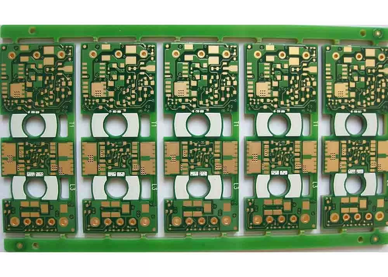
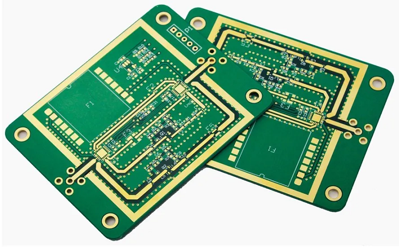
Vias Plugged PCB has become a common technique to improve the integrity and functionality of a board in the world of PCB (Printed Circuit Board) manufacturing. This process involves filling or sealing the holes, known as vias, which are used to create electrical connections between different layers of a PCB. But why is via plugging so important, and what does it involve? In this blog, we’ll dive into what via plugging is, the different types of vias, and its role in PCB design and performance. Let’s explore the various aspects of this technique and its significance in the world of PCB production.

What is Via Plugging in PCB?

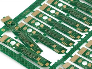
Via plugging is the process of filling or sealing vias, which are holes drilled into a PCB to establish electrical connections between different layers. These vias can be plugged for various reasons, such as preventing unwanted signals from traveling through the vias or ensuring better protection against environmental factors like moisture. The plugging material used may vary, but most commonly, it’s a resin, green oil, or solder mask. The plugged vias add structural integrity to the PCB and enhance its electrical performance.

What Are the Different Types of Vias in PCB?

PCBs can have several types of vias, each designed for specific purposes. The main types include:

Through-hole Vias: These are the most common vias, which pass through the entire board and connect all the layers.

Blind Vias: These connect an outer layer to one or more inner layers but do not pass through the whole PCB.

Buried Vias: These are located entirely within the PCB and do not reach the outer layers, offering a more compact design.

Micro Vias: Smaller than standard vias, they are used in high-density interconnects (HDI) PCBs to create intricate circuits.

Each type of via has its own purpose and is selected based on the design requirements of the PCB.

What’s the Purpose of Vias in PCB?

Vias serve several critical functions in PCB design. Their primary purpose is to provide electrical connections between different layers of the board. This allows signals to travel between top, bottom, and inner layers, creating complex and multi-layer circuits. Vias are also essential for thermal management, helping to dissipate heat across the PCB, ensuring it operates efficiently and remains within temperature limits.

What is the Difference Between Via Plug and Via Fill?

While both processes involve filling vias, they are slightly different in their application. Via plugging refers to sealing the via to prevent signal interference or to fill the via with a non-conductive material, such as resin or solder mask. Via filling, on the other hand, is typically done with a conductive material to ensure that the via still maintains an electrical connection, especially in high-frequency or high-performance PCBs.

What is the Difference Between Tented Via and Untented Via?

A tented via is a via that is sealed with a solder mask over the hole to protect it from environmental damage. This method is often used to prevent moisture or contaminants from entering the via. On the other hand, an untented via remains open and unsealed. Tented vias are commonly used in consumer electronics where the environment is relatively controlled, while untented vias may be seen in applications where electrical continuity is more critical than protection.

What is the Difference Between a PCB Hole and a Via?

The primary difference between a PCB hole and a via lies in their function. A PCB hole is simply a hole in the board, often used for mechanical purposes, such as mounting or securing components. A via, however, is specifically designed for electrical connections between the different layers of the PCB. While holes can be part of a PCB design, vias play a much more specific and functional role in the overall circuit design.

Do Vias Increase PCB Cost?

Yes, vias can increase the cost of manufacturing a PCB. The more complex the via design (e.g., blind or buried vias), the higher the cost due to the additional drilling and processing required. Moreover, the use of via plugging materials, such as resins or green oil, also adds to the cost. However, despite the cost increase, vias are often necessary for high-performance PCBs, especially those used in complex electronics, where the design requirements outweigh the cost considerations.

When to Use Vias in PCB?

Vias are used in PCBs when there’s a need for multi-layered designs or when connecting different electrical components across multiple layers is required. They are often used in high-density and high-frequency PCBs, such as those found in smartphones, computers, and medical devices. If you are designing a PCB that needs to be compact but complex, vias will be essential for providing the necessary electrical connections without compromising space.

Via plugging is an essential process in PCB manufacturing that contributes to both the functionality and durability of the board. Whether you’re working with through-hole, blind, buried, or micro vias, plugging them at the right time and with the right materials ensures that your PCB will perform optimally. By understanding the different types of vias and how they contribute to the overall design, you can make more informed decisions about when and how to use them in your PCB projects.

At EBest Circuit (Best Technology), we specialize in high-quality PCB manufacturing, offering a range of solutions for your project needs. From via plugging to precision design, we ensure that every PCB we produce meets the highest standards of performance and reliability. If you’re looking for a trusted partner for your PCB needs, reach out to us today at sales@bestpcbs.com!

You may also like

What Makes FR4 4 Layer PCB Ideal for Modern Electronics?
Wednesday, January 8th, 2025

FR4 4 layer PCB is a crucial component in modern electronics, offering a blend of durability, reliability, and efficiency. Built using flame-retardant FR4 material, these multilayer boards are designed to handle complex circuits while maintaining excellent performance. Their unique structure, with multiple conductive and insulating layers, supports advanced applications in high-speed and high-density designs. This blog explores the features, structure, and benefits of FR4 4-layer PCBs, answering key questions to provide a clear understanding of their role in electronic manufacturing.

What is FR4 PCB?

FR4 PCB refers to a printed circuit board made from a material called FR4. This material is a type of fiberglass-reinforced epoxy laminate that is widely used in the electronics industry. Its name, FR4, stands for “Flame Retardant 4,” which indicates its excellent fire-resistant properties. FR4 is highly valued for its strength, lightweight nature, and ability to withstand high temperatures. These qualities make it ideal for manufacturing PCBs, which serve as the backbone of electronic devices.

FR4 is not just a material; it is the standard for most PCB substrates. Its insulating properties help protect circuits from electrical interference, while its rigidity provides stability to the board. In the world of electronics, FR4 has become synonymous with reliability and performance.

Is FR4 Electrically Conductive?

No, FR4 is not electrically conductive. It is an insulating material, which is one of its most critical features. This non-conductive nature allows it to act as a barrier between different layers of a PCB, ensuring that electrical signals remain confined to their intended paths. This property is essential for preventing short circuits and signal interference.

The non-conductive nature of FR4 ensures that it can be used in multilayer PCBs without compromising performance. Manufacturers rely on its insulating capabilities to create intricate designs that support complex electronic systems. Its ability to maintain electrical isolation while providing mechanical support makes it indispensable in the industry.

What is a 4-Layer PCB?

A 4-layer PCB is a type of multilayer printed circuit board that consists of four distinct layers of conductive material. These layers are separated by insulating materials like FR4 and are laminated together to form a single board. The typical structure includes two outer layers and two inner layers, each serving specific purposes such as signal transmission, grounding, or power distribution.

4-layer PCBs are commonly used in devices that require compact designs and advanced functionality. They provide enhanced performance compared to single-layer or double-layer PCBs, making them suitable for high-speed circuits and applications with stringent space constraints. Their structure allows for efficient routing, reduced electromagnetic interference, and improved overall performance.

What is a 4-Layer PCB Structure?

The structure of a 4-layer PCB is carefully designed to optimize performance and functionality. Typically, the layers are arranged as follows:

Top Layer (Signal Layer): This is where most of the components are mounted, and primary signal routing occurs.

Inner Layer 1 (Ground Plane): Dedicated to grounding, this layer helps reduce noise and electromagnetic interference.

Inner Layer 2 (Power Plane): This layer is used for power distribution, ensuring consistent voltage levels across the board.

Bottom Layer (Signal Layer): Similar to the top layer, this is used for additional signal routing and component placement.

The separation of power and ground layers helps in maintaining signal integrity and minimizing interference. The insulating layers, often made of FR4, ensure electrical isolation between the conductive layers, enabling reliable and stable operation.

How Thick is 4 Layers of PCB?

The thickness of a 4-layer PCB can vary depending on its design and application. Generally, the total thickness ranges from 0.4mm to 3.2mm. The most common thickness for standard 4-layer PCBs is around 1.6mm, which balances durability and flexibility.

The choice of thickness depends on factors such as the number of components, the complexity of the circuit, and the intended use of the board. Thicker boards offer more mechanical strength, while thinner boards are suitable for compact devices. The use of FR4 as the core material ensures that even thin boards maintain their rigidity and reliability.

What is the Standard Thickness of a Copper Layer on a PCB?

The standard thickness of a copper layer on a PCB is typically measured in ounces per square foot. For most 4-layer PCBs, the standard copper thickness is 1 ounce per square foot, which translates to approximately 35 microns. However, depending on the application, this thickness can be increased to 2 ounces or more for high-current designs.

Copper thickness plays a crucial role in determining the current-carrying capacity and thermal management of the PCB. Thicker copper layers are often used in power distribution layers to handle higher currents, while thinner layers are sufficient for signal transmission.

How to Route a 4-Layer PCB?

Routing a 4-layer PCB requires careful planning and adherence to design principles. The process typically involves the following steps:

Define Layer Functions: Assign specific roles to each layer, such as signal routing, grounding, or power distribution.

Use Ground and Power Planes: Dedicate inner layers to ground and power planes to reduce noise and improve signal integrity.

Minimize Crosstalk: Maintain adequate spacing between traces to prevent signal interference.

Optimize Trace Widths: Ensure trace widths are appropriate for the current-carrying requirements.

Follow Design Rules: Adhere to industry standards and guidelines to ensure manufacturability and performance.

Software tools like PCB design software can assist in creating efficient layouts. By carefully considering the layer stackup and routing strategy, designers can achieve optimal performance and reliability.

Why is FR4 Used in PCBs?

FR4 is widely used in PCBs because of its exceptional properties. It offers high mechanical strength, excellent thermal stability, and reliable electrical insulation. These qualities make it suitable for a wide range of applications, from consumer electronics to industrial machinery.

Its lightweight nature and ease of fabrication further contribute to its popularity. FR4 can withstand high temperatures and resist moisture, ensuring durability in harsh environments. Moreover, its cost-effectiveness makes it an attractive choice for manufacturers, enabling them to produce high-quality PCBs without significantly increasing costs.

In conclusion, FR4 remains a cornerstone material in PCB manufacturing due to its unmatched combination of performance, reliability, and affordability. Its versatility ensures that it will continue to play a pivotal role in the advancement of electronic technologies. At EBest Circuit (Best Technology), we pride ourselves on delivering multiple types of FR4 4 layer PCB products that meet your high-quality standards while maintaining fast delivery times. For more information or any inquiry, warm welcome to reach out to us at sales@bestpcbs.com.
You may also like

What is remote control PCB? PCB Design & Production
Tuesday, January 7th, 2025

What is remote control PCB? The remote control PCB is an electronic circuit board inside the remote control, which is used to connect and support various electronic components to realize signal transmission and processing. It connects the microcontroller, communication module, input components, and power management components through conductive lines, so that the remote control can receive the user’s input signal, convert it into a control signal, and realize remote control of equipment such as TVs and air conditioners.

What is remote control PCB? PCB Design & Production

What is remote control PCB?

The remote control PCB refers to the printed circuit board used in the remote control. It is the core component inside the remote control, responsible for connecting various electronic components to realize various functions of the remote control.

The remote control PCB is usually composed of multiple layers of conductive metal (usually copper foil) and insulating materials. These metal layers are designed into a complex circuit network, and the combination of wiring and insulating materials enables electronic components to achieve electrical connection and functional integration.

The electronic components on the PCB include resistors, capacitors, transistors, integrated circuits (ICs), etc. They are connected together through the metal network on the PCB to form a complete circuit, thereby realizing various functions of the remote control.

The types of remote control PCB mainly include single-sided board, double-sided board and multi-layer board:

  • Single-sided board: the most basic PCB type, suitable for simple circuit design.
  • Double-sided board: wiring on both sides, suitable for more complex circuit design.
  • Multi-layer board: can be further divided into middle and bottom boards and high-layer boards, mainly used for high-end equipment.

Remote control PCB is widely used in various electronic devices. Through the design and layout of PCB, the reception, processing and output of remote control signals can be realized, so as to control the switch, volume adjustment, channel selection and other functions of related equipment.

How to design remote control PCB?

Designing remote control PCB requires comprehensive consideration of functional requirements, component selection, circuit design, layout and wiring, power management, signal integrity, electromagnetic compatibility and thermal design.

What is remote control PCB? PCB Design & Production

1. Functional requirements analysis

  • Determine the control function: clarify which devices and functions the remote control needs to control, such as switch, volume adjustment, channel switching, etc.
  • Signal transmission method: Select a suitable signal transmission method, select the corresponding components and design layout according to the signal type.

2. Component selection

  • Microcontroller (MCU): Select a suitable MCU, and select an MCU with sufficient processing power and input/output interface according to functional requirements.
  • Communication module: Select the corresponding communication module according to the signal type, such as infrared transmission module, radio frequency module or Bluetooth module.
  • Input component: Select a suitable button, touch screen or other input component for user operation and control.
  • Power management component: Select a suitable power management component, such as battery management chip, voltage regulator, etc., to ensure a stable power supply.

3. Circuit design

  • Draw a circuit schematic: Use circuit design software (such as Altium Designer, Eagle, etc.) to draw a circuit schematic and connect all components according to functional requirements.
  • Check the circuit: Carefully check the circuit schematic to ensure that all connections are correct, there are no short circuits or open circuits, etc., and perform circuit analysis and simulation to verify the feasibility of the circuit.

4. PCB layout and wiring

  • Layout: PCB layout should be carried out according to the schematic diagram, and the position of components should be arranged reasonably to minimize signal interference and noise. High-frequency components and sensitive components should be kept away from power lines and ground lines.
  • Wiring: When wiring PCB, try to use short and straight lines to avoid long lines and too many corners. Pay attention to the layout of signal lines and ground lines to ensure stable signal transmission.
  • Impedance matching: For high-frequency signal lines, impedance matching design should be carried out to reduce signal reflection and interference and improve the reliability of signal transmission.

5. Power supply design

  • Power supply circuit: Design a reasonable power supply circuit, including power input, filtering, voltage regulation and other parts to ensure stable power supply and avoid the influence of power supply noise on the circuit.
  • Power management: Design a power management strategy according to the power consumption requirements of the remote control to extend battery life.

6. Signal integrity and electromagnetic compatibility

  • Signal integrity: For high-speed and high-frequency signals, perform signal integrity analysis and design, optimize signal transmission paths, reduce signal distortion and reflection, and ensure signal integrity.
  • Electromagnetic compatibility (EMC): Take measures to improve the electromagnetic compatibility of PCB, reduce electromagnetic interference and radiation, and meet relevant EMC standards.

7. Thermal design

  • Heat dissipation design: According to the power consumption and heat dissipation requirements of the components, perform heat dissipation design, reasonably arrange heat dissipation components, and ensure that the components are within the normal operating temperature range.
  • Thermal management: Use thermal management strategies to improve the heat dissipation performance of PCB.

8. Testing and verification

  • Functional test: Perform functional test on remote control PCB to ensure that all functions work properly, including signal transmission, input response, etc.
  • Performance test: Perform performance test to ensure that the performance of PCB meets the design requirements.
  • Reliability test: Perform reliability test, such as vibration test, temperature cycle test, etc., to ensure the reliability and stability of PCB in various environments.

What does the remote control PCB consist of?

The main components of remote control PCB include mainboard, remote control chip, battery interface, button, indicator light and shell. Among them, the motherboard is the core part of the entire circuit board, and the remote control chip is an important part of controlling the remote control.

  • Motherboard: The core part of the circuit board, carrying other electronic components.
  • Remote control chip: Process key signals, encoding signals and control other circuit components.
  • Battery interface: Provide power support for other components on the circuit board.
  • Key module: Receive user operation instructions and convert the instructions into electrical signals.
  • Indicator light: Display the status or function of the remote control.
  • Shell: Protect internal components and provide users with a grip.

How does a remote control PCB work?

The working principle of the remote control PCB mainly involves signal generation, transmission and reception.

1. User input

  • Button or touch screen operation: The user selects the function or command to be controlled by pressing a button or touching the screen. These input devices convert the user’s operation into electrical signals and send them to the microcontroller (MCU).
What is remote control PCB? PCB Design & Production

2. Signal processing

  • Microcontroller processing: After receiving the input signal, the microcontroller processes and encodes the signal according to the preset program logic.
  • Coding: Control signals are usually encoded into a specific format for easy transmission and identification. The encoded signal contains complete information required for device control.

3. Signal transmission

  • Infrared transmission: For infrared remote control, MCU sends the encoded signal to the infrared transmitting module, which converts the electrical signal into an infrared light signal and transmits it through the infrared transmitting diode.
  • RF transmission: For RF remote control, MCU sends the encoded signal to the RF module, which modulates the signal to a specific frequency and transmits it. RF signals have stronger penetration and longer transmission distance.
  • Bluetooth transmission: For Bluetooth remote control, MCU transmits the signal to the receiving device wirelessly through the Bluetooth module, which is responsible for signal modulation, encoding and transmission.

4. Signal reception

  • Receiving device: The receiving device (such as TV, air conditioner, etc.) is equipped with a corresponding receiving module to receive the signal sent by the remote control.
  • Decoding and execution: After receiving the signal, the receiving module decodes it, converts it into a control instruction, and then performs the corresponding operation according to the instruction.

Through the above steps, the remote control PCB realizes the complete process from user input to device control, enabling users to conveniently operate various devices remotely.

How to produce remote control PCB?

The production process of remote control PCB mainly includes the following steps:

  • Design stage: The design stage includes determining the function of the circuit, laying out components, drawing wire paths, etc.
  • Raw material preparation: According to the design requirements, purchase suitable substrate materials, such as FR-4, which has good insulation, mechanical strength and cost-effectiveness, and is suitable for most common electronic products.
  • Cutting and drilling: Cut the copper clad board into the required size, and use a high-precision drilling machine to drill precise through holes on the circuit board. These holes will be used for electrical connections between different layers.
  • Copper deposition: The hole wall of the PCB is bulked to enhance adhesion, and then a copper foil layer is deposited on the hole wall by electrochemical method to ensure the conductivity of the hole.
  • Line exposure: Use LDI technology to accurately project the circuit diagram onto the copper clad layer of the PCB, and form the prototype of the circuit diagram through exposure and development of the photosensitive dry film.
  • Electroplating: Further increase the thickness of the copper layer on the developed circuit and hole wall to ensure its conductivity and mechanical strength.
  • Outer layer etching: Etch the outer layer of the PCB to form the required circuits and pads.
  • Gold treatment: Perform gold treatment on the exposed key PAD position to protect the copper layer and prevent oxidation.
  • Shape treatment: Perform shape treatment on the PCB substrate and finally complete the production.

What should we pay attention to during the production of remote control PCB?

In the production process of remote control PCB, the following key aspects need to be paid attention to to ensure product quality and performance:

1. Design stage

  • Design review: Ensure that the circuit design is correct and meets the functional and manufacturing requirements.
  • Follow standards: Strictly follow industry standards and specifications, such as IPC standards, to ensure the manufacturability of the design.

2. Material selection

  • High-quality materials: Select substrate materials and copper foil that meet the specifications to ensure good insulation and conductivity.
  • Supplier management: Select suppliers with good reputation to ensure stable and reliable material quality.

3. Manufacturing process

  • Process control: Strictly control key process parameters such as exposure, etching, and lamination to ensure the stability and consistency of the production process.
  • Standard Standardized operation: formulate detailed operating procedures to ensure that operators operate according to unified standards and reduce human errors.

4. Quality inspection

  • Intermediate inspection: set up multiple inspection points during the production process to find and correct problems in time.
  • Finished product inspection: conduct comprehensive finished product inspection, including functional testing, electrical performance testing and appearance inspection, to ensure that the product meets quality standards.
  • Thermal management: rationally layout heat dissipation components and heat dissipation channels to ensure that the components are within the normal operating temperature range.
  • Electromagnetic compatibility: take measures to improve the electromagnetic compatibility of PCB and reduce electromagnetic interference and radiation.

Through the above measures, the production quality of remote control PCB can be effectively improved to ensure its reliability and performance in practical applications.

How to choose a suitable remote control PCB supplier?

Selecting a remote control PCB supplier can be considered from the following points:

1. Comprehensive strength

  • Production capacity: pay attention to the production line, equipment and workers to ensure that the production scale and delivery period can be met, and understand the ability to respond to emergency orders.
  • Technical level: check whether there are advanced process capabilities and R&D teams, and whether they can provide technical support.
  • Quality control: examine whether there are quality certifications and complete testing processes and equipment.
What is remote control PCB? PCB Design & Production

2. Service quality

  • Pre-sales service: see whether it can provide comprehensive technical consultation, respond to needs in a timely manner, and provide quotations and samples.
  • After-sales service: understand the after-sales guarantee policy and team situation.

3. Reputation

  • Customer evaluation: view other customer evaluations through various channels.
  • Industry status: understand its popularity and cooperation in the industry.

4. Price cost

  • Price comparison: compare multiple quotations, pay attention to price composition and long-term cooperation discounts.
  • Cost-effectiveness evaluation: comprehensively consider quality, service, etc. to evaluate cost-effectiveness.

As a professional PCB manufacturer, BEST Technology has strong design and technical support capabilities, and can provide customized remote control PCB design solutions according to customer needs, and ensure reasonable layout and stable signals.

At the same time, we have advanced production equipment and flexible production scale, which can efficiently produce various types of remote control PCBs to meet the needs from small batch proofing to large batch production; in terms of quality control, we follow a strict quality management system and use advanced testing equipment for comprehensive testing to ensure that the quality of each PCB is reliable and defect-free.

In addition, we focus on on-time delivery, provide high-quality customer service and technical support, and respond quickly to customer needs to ensure that customers are worry-free during use and enjoy a good service experience.

You may also like

What Do You Know About Aluminum PCB Prototyping?
Thursday, January 2nd, 2025

Aluminum PCB prototyping has transformed how electronic designs are tested and refined. It offers a reliable way to create high-performance circuits with enhanced thermal management and durability. Whether you’re developing a small batch for testing or a custom design for specific needs, understanding aluminum PCB prototyping is essential. At EBest Circuit (Best Technology), we specialize in offering tailored aluminum PCB solutions with fast delivery and exceptional quality.

What Is an Aluminum PCB?

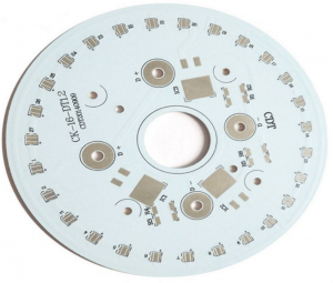
An aluminum PCB is a type of printed circuit board with an aluminum core, which acts as a heat sink. This design improves heat dissipation, making it ideal for high-power applications like LED lighting and automotive systems. Its structure includes an aluminum base, an insulating layer, and copper traces. This combination ensures excellent thermal performance and reliability, especially in demanding environments.

What Is PCB Prototyping?

PCB prototyping is the process of creating a preliminary version of a printed circuit board to test its functionality and design. It allows engineers to identify and correct potential flaws before full-scale production. With advancements in technology, prototyping has become faster and more cost-effective, enabling quick iterations for design improvements.

What Is ASIC Prototyping?

ASIC (Application-Specific Integrated Circuit) prototyping involves creating a functional model of a custom-designed chip. While not directly related to PCBs, it shares similarities in testing and refining designs before mass production. Combining ASIC prototyping with aluminum PCB prototyping can optimize performance in high-frequency or power-intensive applications.

How Much Does a PCB Prototype Cost?

The cost of a PCB prototype depends on several factors, including material, complexity, size, and quantity. Aluminum PCB prototypes are generally more expensive than standard FR4 prototypes due to the specialized materials and processes involved. However, their benefits in thermal management and durability often outweigh the higher initial cost. At EBest Circuit (Best Technology), we offer competitive pricing for small and large-scale prototypes, ensuring value without compromising quality.

How to Make PCB Prototyping?

PCB prototyping involves several steps:

Designing the Circuit: Engineers create a detailed schematic using design software.

Fabrication: The design is transferred onto the aluminum base through processes like etching and drilling.

Assembly: Components are soldered onto the board.

Testing: The prototype undergoes rigorous testing to verify performance.

Advanced tools and precise manufacturing are critical to ensuring the prototype matches the design requirements.

How Do You Make a Circuit with Aluminum Foil?

Creating a simple circuit with aluminum foil is a basic DIY project often used for educational purposes. Aluminum foil serves as the conductive path for electricity. While this method is not suitable for professional applications, it demonstrates the principles of electrical circuits. For real-world use, aluminum PCBs provide far superior performance and reliability.

How Do You Make Aluminum PCB?

Manufacturing an aluminum PCB involves:

Material Preparation: Selecting a high-quality aluminum core.

Lamination: Adding an insulating layer and copper foil.

Patterning: Using photolithography to create the circuit pattern.

Etching: Removing excess copper to form the traces.

Drilling and Plating: Creating holes and coating them with conductive material.

Each step requires precision to ensure the PCB meets technical and thermal specifications.

What Are the Advantages of Aluminum PCB?

Aluminum PCBs are known for their thermal conductivity, durability, and environmental friendliness. They effectively dissipate heat, reducing the risk of component failure. Their robust structure ensures longevity, even in harsh conditions. Additionally, aluminum is recyclable, making these PCBs an eco-conscious choice. With these benefits, aluminum PCBs are widely used in LED lighting, automotive systems, and power electronics.

Why Choose EBest Circuit (Best Technology)?

EBest Circuit (Best Technology) stands out for offering a wide range of products, small quantity orders, and high-quality standards. Our expertise in aluminum PCB prototyping ensures fast delivery and fully customized solutions. We prioritize customer satisfaction by delivering exceptional service and reliable results.

In Conclusion, aluminum PCB prototyping bridges the gap between innovative design and practical application. Its ability to combine thermal performance with reliability makes it a top choice for modern electronics. At EBest Circuit (Best Technology), we are dedicated to supporting your prototyping needs with superior quality and customized solutions. Trust us for your next project, and experience the Best in PCB manufacturing.

You may also like

Ceramic Base PCB, Reliable Ceramic Base PCB Manufacturer
Tuesday, December 31st, 2024

Ceramic base PCB is gaining popularity due to their exceptional performance in challenging environments. As a leading ceramic base PCB manufacturer, EBest Circuit (Best Technology) takes pride in offering top-quality solutions for a wide range of applications. This blog explores ceramic base PCBs, their benefits, applications, types, materials, design considerations, and why EBest Circuit (Best Technology) stands out as the ideal partner for your PCB needs.

What Is Ceramic Base PCB?

A ceramic base PCB uses ceramic materials as its substrate instead of traditional options like FR4. These PCBs are renowned for their excellent thermal conductivity, electrical insulation, and mechanical stability. Designed for high-performance applications, they excel in environments requiring durability and precision.

Ceramic base PCB is often chosen for industries like aerospace, automotive, and medical devices, where reliability and efficiency are paramount. Its unique properties make them indispensable for cutting-edge technologies.

What Are The Benefits of Ceramic Base PCB?

Ceramic base PCBs offer several advantages that set them apart from conventional options. Their high thermal conductivity ensures efficient heat dissipation, making them ideal for power-intensive devices. Their low coefficient of thermal expansion minimizes the risk of mechanical stress, ensuring long-lasting performance.

These PCBs are also highly resistant to chemical and environmental damage. Their excellent electrical insulation supports stable and reliable operations, even under challenging conditions. Combined with their compact size and lightweight nature, ceramic base PCBs are a top choice for innovative and efficient electronic designs.

What Are The Applications of Ceramic Base PCBs?

Ceramic base PCBs find applications across various industries due to their superior properties. In the automotive sector, they are used in engine control systems and LED lighting. Aerospace applications include navigation systems and avionics, where reliability is critical.

In the medical field, ceramic base PCBs are essential for diagnostic devices, imaging systems, and surgical instruments. They are also widely employed in telecommunications for RF and microwave components. Consumer electronics, including LED displays and sensors, further benefit from their durability and efficiency.

What Are The Different Types of Ceramic Base PCB?

Ceramic base PCBs are available in several types, each designed to meet specific requirements:

Aluminum Nitride (AlN) PCBs: Known for high thermal conductivity and excellent electrical insulation.

Alumina (Al2O3) PCBs: Cost-effective and suitable for a wide range of applications.

Beryllium Oxide (BeO) PCBs: Exceptional thermal performance, though less commonly used due to safety concerns.

Silicon Nitride (Si3N4) PCBs: High strength and thermal shock resistance, ideal for demanding environments.

Each type offers unique features to suit different industries and applications.

Why Turn To EBest Circuit (Best Technology) For Ceramic Base PCB?

EBest Circuit (Best Technology) is a trusted name in the PCB manufacturing industry, offering unmatched expertise in ceramic base PCBs. We cater to diverse customer needs with our wide product range, including various types of ceramic PCBs. Whether you require small quantities or bulk orders, our flexible production capabilities ensure your demands are met efficiently.

Our focus on quality is unwavering. Every product undergoes stringent testing to meet the highest standards. We prioritize fast delivery, ensuring your projects stay on schedule. With our customization services, you can rely on us for tailored solutions that fit your specific requirements. Our commitment to exceptional service makes us the preferred choice for customers worldwide.

What Is the Material of Ceramic Base PCB?

The materials used in ceramic base PCBs are critical to their performance. Common materials include:

Aluminum Nitride (AlN): Offers outstanding thermal conductivity and is ideal for high-power applications.

Alumina (Al2O3): Provides a balance of performance and cost-effectiveness, making it widely popular.

Beryllium Oxide (BeO): Delivers superior thermal performance but requires careful handling.

Silicon Nitride (Si3N4): Combines strength, thermal resistance, and reliability.

These materials are chosen based on application requirements, ensuring optimal performance and durability.

How To Design Ceramic Base PCB?

Designing ceramic base PCBs requires careful consideration of material properties, thermal management, and circuit layout. The substrate’s thermal conductivity must align with the application’s heat dissipation needs. Selecting appropriate components and ensuring proper spacing is essential for reliable operation.

Advanced fabrication techniques, such as laser drilling and metallization, are used to achieve precision and quality. Working with experienced manufacturers like EBest Circuit (Best Technology) ensures that every aspect of your design is optimized for performance and longevity.

FAQs About Ceramic Base PCB

1. What industries use ceramic base PCBs?

Industries like automotive, aerospace, medical devices, telecommunications, and consumer electronics widely use ceramic base PCBs.

2. How does ceramic base PCB compare to traditional PCBs?

Ceramic base PCBs offer superior thermal conductivity, mechanical strength, and environmental resistance compared to traditional PCBs.

3. Can ceramic base PCBs be customized?

Yes, EBest Circuit (Best Technology) provides fully customized ceramic base PCBs to meet unique application requirements.

4. What is the lead time for ceramic base PCBs?

With our fast delivery services, lead times are minimized, ensuring your projects stay on track. Normally, The fastest lead time is about 2 weeks.

5. Why is thermal conductivity important in ceramic base PCBs?

High thermal conductivity ensures efficient heat dissipation, critical for maintaining performance in high-power applications.

In short, ceramic base PCBs are indispensable for industries requiring high performance and reliability. EBest Circuit (Best Technology) excels in delivering top-notch ceramic base PCBs tailored to your needs. With our diverse product range, exceptional quality, and fast delivery, we are your trusted partner for ceramic base PCB solutions. If you have any questions or any inquiry about ceramic base PCB products, warm welcome to consult us via sales@bestpcbs.com. Thank you.
You may also like

Aluminum PCB LED, Aluminum Base PCBs for LEDs
Tuesday, December 31st, 2024

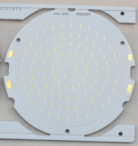
An aluminum PCB LED refers to a specialized printed circuit board (PCB) that uses an aluminum base to support and enhance LED (Light Emitting Diode) applications. These PCBs are specifically designed to manage the heat generated by LEDs during operation. In essence, an aluminum PCB LED combines the benefits of advanced circuit design with excellent thermal conductivity, ensuring optimal performance for LED systems.

Aluminum PCBs have revolutionized LED lighting by addressing heat dissipation challenges. These circuit boards, crafted with an aluminum base, deliver excellent thermal management, durability, and efficiency. This blog explores their material composition, thermal properties, and significance in LED applications. Whether you’re designing LED systems or curious about the advantages of aluminum PCBs, this comprehensive guide offers valuable insights.

What Is the LED of Aluminum?

LEDs mounted on aluminum PCBs are essential for applications demanding high efficiency and longevity. The aluminum base acts as a thermal conductor, transferring heat away from the LED components. This process enhances the lifespan and performance of LEDs, particularly in high-power applications like floodlights and automotive lighting. These PCBs are also lightweight, making them suitable for compact designs.

What Is the Material of Aluminum PCB?

Aluminum PCBs typically consist of three layers:

1. Base Layer: Made of aluminum, this layer provides structural support and excellent heat dissipation.

2. Dielectric Layer: Positioned between the base and the circuit layer, it ensures electrical insulation while conducting heat.

3. Circuit Layer: Copper circuits are etched onto this layer to form the electrical connections.

The combination of aluminum and copper enhances conductivity and thermal efficiency. These materials make aluminum PCBs reliable for LED applications.

What Temperature Can Aluminum PCB Withstand?

Aluminum PCBs are designed to operate in high-temperature environments. They can typically withstand temperatures between 120°C and 150°C, depending on the design and material quality. High thermal resistance ensures consistent performance, even in demanding applications like outdoor LED lighting and automotive headlights. Selecting the right PCB thickness and dielectric material is critical for optimizing thermal tolerance.

What Is the Thermal Resistance of Aluminum PCB?

The thermal resistance of an aluminum PCB is the measure of its heat transfer capability. It typically ranges between 1.0°C/W and 2.0°C/W, depending on the board’s structure and material quality. Lower thermal resistance indicates better heat dissipation, which is essential for high-power LEDs. Aluminum PCBs achieve this through their unique combination of metal cores and dielectric materials.

How Thick Is Aluminum PCB?

Aluminum PCBs vary in thickness to suit different applications. Common thicknesses include:

Base Layer: Typically 1.0mm to 2.0mm.

Dielectric Layer: Around 0.075mm to 0.15mm.

Circuit Layer: Common circuit layer thickness is about 0.035mm‌.

The choice of thickness depends on the required mechanical strength, heat dissipation, and electrical load. Thicker boards are ideal for heavy-duty applications like industrial LED lighting.

What Is the Difference Between Copper and Aluminum PCB?

Copper and aluminum PCBs serve similar purposes but have distinct characteristics:

Thermal Conductivity: Copper PCBs offer higher conductivity, while aluminum PCBs balance thermal performance and cost.

Weight: Aluminum PCBs are lighter, making them ideal for compact designs.

Cost: Aluminum PCBs are generally more affordable than copper-based alternatives.

Aluminum PCBs are preferred for LED applications due to their efficient heat dissipation and lower production costs.

How Do You Connect LED to PCB?

Connecting LEDs to aluminum PCBs involves precise soldering. Here’s a simplified process:

1. Prepare the PCB: Clean the board and check the circuit layout.

2. Place the LED: Align the LED pins with the PCB pads.

3. Solder the Connections: Use a soldering iron to secure the LED.

4. Test the Circuit: Verify functionality with a power supply.

Aluminum PCBs are designed to handle heat generated during soldering, ensuring durability and reliable connections.

Why Use Aluminum PCB?

Aluminum PCBs are preferred for LED applications due to several reasons:

1. Heat Management: They efficiently dissipate heat, ensuring LEDs operate at optimal temperatures.

2. Durability: Aluminum provides structural strength and resistance to wear.

3. Lightweight: The boards are easy to integrate into compact devices.

4. Energy Efficiency: They reduce thermal losses, improving overall efficiency.

These features make aluminum PCBs a cornerstone in modern LED lighting solutions, from consumer electronics to industrial systems. EBest Circuit (Best Technology)’s competitive edge lies in its ability to deliver multiple types of products, customized to your needs, with fast delivery and unmatched quality.

What are Applications of Aluminum PCBs in LEDs?

Aluminum PCBs (Printed Circuit Boards) are widely used in LED applications due to their excellent thermal management properties. Here are the main applications of aluminum PCBs in LEDs:

1. High-Power LED Lighting: Aluminum PCBs are ideal for high-power LED lighting systems, such as streetlights, floodlights, and spotlights. The metal core provides effective heat dissipation, preventing LEDs from overheating and improving their efficiency and lifespan.

2. LED Modules for Displays: Aluminum PCBs are used in LED modules for large-scale digital displays, such as billboards and signage. The thermal management capacity of aluminum ensures the stability of the LEDs during continuous operation.

3. Automotive Lighting: In automotive lighting systems, aluminum PCBs are used for headlights, tail lights, and interior lighting. The ability of aluminum to manage heat is critical to maintain LED performance and prevent failure in harsh automotive environments.

4. Backlighting for LCD Displays: Aluminum PCBs are used in the backlight systems of LCD displays, such as those in TVs, monitors, and smartphones. The heat dissipation capabilities enhance the longevity and reliability of the LEDs used for backlighting.

In each of these applications, aluminum PCBs help to reduce the risk of overheating, enhance the performance of LEDs, and extend their operational life, making them a preferred choice for various LED-based lighting and display systems.

In conclusion, aluminum PCBs are indispensable for high-performance LED applications. Their superior thermal management, lightweight construction, and cost-effectiveness provide unparalleled benefits. Choosing the right aluminum PCB for your LED projects ensures durability and efficiency. If you need customized solutions, EBest Circuit (Best Technology) offers premium aluminum PCB led tailored to your requirements. Just feel free to contact us via sales@bestpcbs.com.
You may also like

Why Ceramic Substrate PCB Is Gaining Popularity?
Monday, December 30th, 2024

Ceramic substrate PCB is a crucial component in modern electronics, offering significant advantages in applications requiring high thermal conductivity, electrical insulation, and mechanical strength. In this blog, we will delve into the various aspects of ceramic substrate PCB, explaining its materials, benefits, and applications, and explore how it compare to traditional FR4-based PCB. Whether you are new to PCB design or an experienced engineer, this guide will help you understand why ceramic substrate PCB is gaining popularity.

What is Ceramic Substrate PCB?

Ceramic substrate PCB or ceramic PCB is a type of printed circuit board that uses ceramic materials as the base substrate. Unlike traditional PCBs, which are usually made of fiberglass (FR4), ceramic substrate PCB is designed to handle high thermal stresses and provide better electrical insulation properties. This PCB is commonly used in industries like telecommunications, automotive, medical devices, and power electronics due to their exceptional thermal management capabilities and durability.

The main advantage of ceramic substrate PCBs is their ability to dissipate heat efficiently, which is vital in applications where heat management is a critical factor. Ceramic materials, such as alumina (Al₂O₃), aluminum nitride (AlN), and beryllium oxide (BeO), are known for their excellent heat conductivity, making them ideal for high-power electronics.

What is the Best Substrate for PCB?

The best substrate for a PCB depends on the specific application and the requirements of the circuit. For general-purpose electronics, FR4 is the most commonly used substrate due to its balance of cost and performance. However, for applications that demand superior thermal conductivity, high-frequency performance, or electrical insulation, ceramic substrates are often the preferred choice.

Ceramic substrates are especially suitable for high-power, high-frequency, and high-temperature environments. These materials offer lower thermal expansion rates, higher thermal conductivity, and better resistance to extreme conditions than traditional PCB materials. Therefore, in scenarios where heat management is paramount, such as power amplifiers or LED lighting, ceramic PCBs are the best option.

What Material is Commonly Used for PCBs?

The material commonly used for PCBs can vary depending on the application. The most popular materials include:

FR4 (Fiberglass Reinforced Epoxy): This is the most common PCB material, primarily used for general electronic applications. It is affordable and offers decent mechanical and electrical properties.
Ceramic: As discussed, ceramic materials such as alumina, aluminum nitride, and beryllium oxide are used in high-performance PCBs. They are particularly suited for thermal management and high-frequency applications.
Polyimide: Used for flexible PCBs, polyimide provides excellent resistance to heat and harsh chemicals.
Teflon: Ideal for high-frequency circuits, Teflon offers low signal loss and excellent electrical insulation.

While FR4 is suitable for most basic applications, ceramic substrates stand out when specific performance characteristics like high thermal conductivity or resistance to high temperatures are needed.

Which PCB Substrate Has High Thermal Conductivity?

Ceramic PCBs are known for their superior thermal conductivity compared to other PCB materials. Materials like aluminum nitride (AlN) and boron nitride (BN) have the highest thermal conductivity, making them ideal for high-power applications where heat dissipation is crucial.

Aluminum nitride, for instance, offers thermal conductivity values between 170-200 W/mK, which is significantly higher than that of FR4, which typically ranges around 0.3 W/mK. This makes ceramic substrates the go-to choice for applications such as power electronics, LED lights, and other high-heat applications where heat needs to be efficiently transferred away from the components.

What is the Thermal Conductivity of Ceramic PCB?

The thermal conductivity of ceramic PCBs can vary depending on the material used. The most common ceramic materials include:

Alumina (Al₂O₃): This is one of the most frequently used materials in ceramic PCBs. Alumina has a thermal conductivity ranging from 20 to 30 W/mK, making it suitable for medium-to-high-power applications.
Aluminum Nitride (AlN): Aluminum nitride has a much higher thermal conductivity, typically around 170-200 W/mK. This makes it ideal for high-power applications, especially in areas where rapid heat dissipation is needed.
Beryllium Oxide (BeO): While less commonly used due to safety concerns (due to the toxic nature of beryllium), Beryllium oxide offers very high thermal conductivity, around 250-300 W/mK.

When compared to other PCB materials, ceramic substrates offer a distinct advantage in terms of their heat management capabilities. They ensure that sensitive components remain within their operating temperature range, extending their lifespan and improving performance.

How Thick is Ceramic PCB?

The thickness of a ceramic PCB can vary depending on the design requirements and the specific material used. Typically, ceramic PCBs can range from 0.2 mm to 2 mm in thickness, but in some cases, they can be made thicker or thinner to suit specific needs.

The thickness of the PCB plays a role in both its mechanical strength and thermal properties. Thicker ceramics tend to offer better heat dissipation, but they may be more rigid and difficult to process. On the other hand, thinner ceramics are more flexible but may not handle as much thermal stress. The optimal thickness depends on the application and the required performance characteristics of the circuit.

What is the Difference Between Ceramic Substrate and FR4?

The primary difference between ceramic substrates and FR4 PCBs lies in their material properties and performance characteristics.

Thermal Management: Ceramic substrates excel in heat dissipation, with materials like aluminum nitride offering significantly higher thermal conductivity than FR4. This makes ceramics the better choice for high-power applications.
Electrical Insulation: Ceramic substrates provide superior electrical insulation compared to FR4, making them ideal for applications requiring high voltage isolation.
Mechanical Properties: Ceramic PCBs are often more rigid and can withstand higher temperatures than FR4-based boards, making them suitable for demanding environments.
Cost: FR4 is much cheaper to produce than ceramic substrates, making it the go-to material for mass-produced electronics. However, when performance is the priority, ceramic PCBs provide a much better solution, despite their higher cost.

Overall, the choice between ceramic and FR4 substrates depends on the specific needs of the project. If thermal management, high-frequency performance, or electrical insulation is critical, ceramic substrates are often the better option.

What is Ceramic Board Used For?

Ceramic boards, or ceramic PCBs, are widely used in applications where thermal conductivity, electrical insulation, and mechanical strength are critical. Some of the most common applications of ceramic PCBs include:

Power Electronics: Ceramic PCBs are used in power supplies, inverters, and other high-power circuits, where heat dissipation is crucial for reliable operation.
LED Lighting: Ceramic substrates are used in LED modules, where efficient heat management is essential for preventing thermal damage to the LEDs and improving their lifespan.
Telecommunications: In high-frequency communication equipment, ceramic PCBs help ensure signal integrity and manage heat effectively.
Automotive: Ceramic PCBs are used in automotive electronics, including control systems, power modules, and sensors, which require high thermal conductivity and reliability in harsh environments.
Medical Devices: Ceramic PCBs are used in medical devices such as MRI machines and pacemakers, where high precision and reliability are essential.

The versatility of ceramic PCBs makes them an excellent choice for any application where performance, thermal management, and durability are essential.

Ceramic substrate PCBs play a vital role in modern electronics, offering superior thermal conductivity, electrical insulation, and mechanical strength compared to traditional FR4-based boards. They are essential in high-power, high-frequency, and high-temperature applications, ensuring that sensitive components operate within their optimal temperature range. While ceramic PCBs tend to be more expensive than FR4, their performance benefits make them the go-to solution for industries where reliability and performance are paramount.

Choosing ceramic PCBs can elevate your designs, particularly when heat management and durability are top priorities. If your application demands top-tier performance, ceramic substrates are a smart investment that ensures long-lasting and efficient operation.

As a ceramic PCB manufacturer, EBest Circuit (Best Technology) specialize in providing high-quality ceramic PCBs tailored to your specific needs. With our advanced manufacturing processes and expert team, we ensure that every PCB we produce meets the highest standards of performance and reliability. If you are looking for dependable ceramic substrate manufacturers, contact us today at sales@bestpcbs.com to learn more about how we can help with your next project.

You may also like

Aluminum Core PCB Material, Aluminum PCB Stackup
Friday, December 27th, 2024

Aluminum Core PCB Material mainly consists of ‌aluminum, copper foil, and an insulating layer‌. Aluminum PCB Stackup refers to the specific layer structure and arrangement of an aluminum-based printed circuit board (PCB)‌.

The most distinguishing feature of an aluminum PCB is its metal core, which is typically made of aluminum. Above the aluminum core, there is an insulating layer made from a high-performance dielectric material. On top of the dielectric layer, there is a copper layer where the circuit traces are etched. In some cases, there is a final protective coating or layer, such as solder mask or a conformal coating, placed over the copper traces. Whether you’re designing a high-performance device or a simple circuit board, understanding the materials and structure behind aluminum PCBs can help you make the right choice.
What is the material of aluminum PCB?

Aluminum PCBs are made primarily from aluminum, a material known for its excellent thermal conductivity, light weight, and high durability. The core of these PCBs is made of a solid aluminum base, which helps in dissipating heat away from the components. This makes them ideal for applications that involve high power and heat generation, such as power supplies, LED lighting, and automotive electronics.

In addition to the aluminum base, the board also includes a layer of insulating material, usually made from epoxy resin or other high-performance substrates. The insulating layer is key to preventing electrical conductivity between the aluminum and the circuit traces.

What is the material of metal core PCB?

Metal core PCBs, often referred to as MCPCBs, are made from a variety of metal materials, with aluminum being the most common. Other metals, such as copper and iron, can also be used for the core. However, aluminum is favored due to its superior thermal conductivity, cost-effectiveness, and ease of fabrication.

The construction of metal core PCBs generally involves three main layers: the metal base, an insulating dielectric layer, and the copper circuitry. The insulating layer separates the metal core from the copper traces, ensuring that the circuit functions as intended while preventing short circuits.

What is PCB core made of?

The PCB core is typically made from a conductive metal base, which is then covered with a layer of insulating material. For aluminum core PCBs, the core is an aluminum sheet, which is highly effective at conducting heat away from the components mounted on the PCB. The aluminum is often coated with a thin layer of insulation, such as an epoxy resin, which helps protect the metal and ensures that electrical components do not come into direct contact with the aluminum.

In more traditional PCBs, the core is often made of materials like FR4 (a fiberglass-based material), which provides mechanical strength and electrical insulation. However, aluminum core PCBs are preferred in applications where heat management is crucial, as aluminum offers far superior heat dissipation properties.

What material is commonly used for PCBs?

The material commonly used for PCBs varies depending on the application and the specific needs of the circuit. Standard PCBs often use materials such as FR4, a composite material made of fiberglass and epoxy resin. This material is inexpensive and easy to work with, making it the most widely used in everyday electronic devices.

However, in high-performance applications, materials with better thermal conductivity, such as aluminum, are used. These are typically referred to as metal core PCBs or MCPCBs. Aluminum, in particular, is a popular choice because of its combination of excellent thermal management and cost-efficiency.

What is the structure of aluminum PCB?

The structure of an aluminum PCB consists of several layers, each serving a specific purpose. The typical stackup includes:

Aluminum Core: The base layer made of aluminum, which provides heat dissipation.

Dielectric Insulating Layer: A layer of insulating material, typically made from epoxy or other high-performance resins, which electrically isolates the metal from the circuit traces.

Copper Layer: The top layer where the circuit traces are etched. This layer is where the components are mounted, and electrical connections are made.

The aluminum core helps dissipate the heat generated by the components, ensuring that the PCB can handle high-power applications without overheating. The insulating layer prevents short circuits by isolating the copper traces from the aluminum base.

Why use aluminum PCB?

Aluminum PCBs are used primarily for their ability to manage heat effectively. In applications where excessive heat is generated, such as in LED lighting systems or power electronics, aluminum PCBs are essential. The aluminum core helps in quickly transferring heat away from sensitive components, preventing damage and ensuring the device operates efficiently for longer periods.

Another benefit of aluminum PCBs is their lightweight nature, which makes them ideal for applications where weight is a consideration. The low cost of aluminum, compared to other materials like copper, also makes aluminum PCBs a more budget-friendly option without compromising on performance.

Furthermore, aluminum PCBs are extremely durable, offering high resistance to physical wear and corrosion. This makes them a good choice for outdoor or harsh environment applications, such as automotive or industrial equipment.

How do you make Aluminum PCB?

Manufacturing an aluminum PCB involves several steps. Below is a simplified process:

Designing the PCB: The first step is designing the PCB using CAD software. This includes specifying the copper traces, component placement, and thermal management requirements.

Creating the Aluminum Base: The aluminum base is cut and shaped to the required size. It is then coated with a thin layer of insulating material to electrically isolate the aluminum from the circuit traces.

Etching the Copper Layer: The copper layer is then applied to the insulating layer, and the circuit traces are etched into the copper using a photolithography process. This step defines the electrical pathways.

Drilling and Component Mounting: Holes are drilled into the PCB to allow for component placement, and the components are then soldered onto the board.

Testing and Inspection: Once assembled, the PCB undergoes thorough testing to ensure it meets quality standards and functions as intended. This includes thermal testing to check the heat dissipation capabilities of the aluminum core.

Aluminum core PCBs are an excellent choice for applications that require efficient heat dissipation and durability. Their unique structure, consisting of an aluminum base, insulating layer, and copper circuitry, makes them ideal for power-hungry devices like LEDs, power supplies, and automotive electronics. Understanding the materials used in aluminum PCBs and the stackup structure can help you make informed decisions when designing your own boards. When it comes to sourcing aluminum PCBs, choosing the right supplier is critical. EBest Circuit (Best Technology) provides high-quality aluminum core PCBs that meet stringent performance standards and are customizable for your specific needs. Reach out to us at sales@bestpcbs.com for more details.

You may also like

Ceramic Multilayer PCB: An In-Depth Guide
Thursday, December 26th, 2024

In the world of printed circuit board (PCB), ceramic PCB stands out as a reliable choice for applications requiring superior thermal conductivity, high-frequency performance, and robust electrical insulation. Ceramic multilayer PCB, in particular, offers an added advantage by combining multiple layers of ceramic material to enhance the performance and reliability of electronic devices. In this article, we’ll explore what ceramic PCBs is, its different types, and its specific advantages compared to other materials like FR4.

What is a Ceramic PCB?

A ceramic PCB is a type of printed circuit board made using ceramic materials instead of traditional fiberglass-based boards. Ceramic substrates are known for their excellent thermal conductivity, high dielectric strength, and resistance to high temperatures. These properties make ceramic PCBs ideal for use in high-performance electronic devices that need to withstand extreme conditions.
Ceramic PCB is widely used in applications like power electronics, automotive electronics, and telecommunications, where heat dissipation and stability are critical. Unlike FR4, which is a common base material for most PCBs, ceramic materials can handle much higher operating temperatures, which is essential in many industrial applications.

What Are the Different Types of Ceramic PCB?

There are several types of ceramic PCBs, each with unique properties that cater to specific needs. Here are the most commonly used:
1. Alumina (Al2O3) PCBs: Alumina ceramic PCBs are the most common type. They are highly versatile and used in various applications, from consumer electronics to medical devices.
2. Aluminum Nitride (AlN) PCBs: Known for their outstanding thermal conductivity, AlN ceramic PCBs are often used in high-power applications like LED lighting, automotive systems, and power supplies.
3. Beryllium Oxide (BeO) PCBs: These PCBs are excellent in terms of thermal conductivity and electrical insulation. They are commonly used in high-frequency applications such as microwave systems.
4. Silicon Nitride (Si3N4) PCBs: These are known for their strength and thermal stability. Silicon Nitride PCBs are often used in devices that require a combination of electrical insulation and heat resistance.
Each type of ceramic material has its own set of advantages, and selecting the right one depends on factors like the operating temperature, power requirements, and the environment in which the PCB will be used.

What is the Difference Between Ceramic Substrate and FR4?

Ceramic substrates and FR4 serve similar functions in PCBs, but they differ in their material properties. FR4 is a glass-reinforced epoxy laminate, typically used in most PCBs due to its cost-effectiveness and ease of fabrication. However, it doesn’t perform well in high-temperature or high-frequency applications.
On the other hand, ceramic substrates, like alumina, have a much higher thermal conductivity and can withstand much higher temperatures, making them ideal for applications that require robust heat management. Additionally, ceramic substrates have superior electrical insulation properties compared to FR4, which is a key factor in high-power and high-voltage circuits.
In short, while FR4 is affordable and effective for everyday applications, ceramic substrates are preferred for demanding environments where thermal management and high-frequency performance are essential.

How Thick is Ceramic PCB?

The thickness of ceramic PCBs can vary depending on the application and the type of ceramic material used. Typically, ceramic PCBs range in thickness from 0.25mm to 3.0mm, but thicker versions are possible for applications requiring more robust structural support or additional layers for signal routing.
The thickness also impacts the overall thermal conductivity of the board. Thicker ceramic PCBs provide better heat dissipation but may also reduce the flexibility for complex circuit designs. Choosing the right thickness is critical to ensure optimal performance and efficiency in the final product.

What is the Thermal Conductivity of Ceramic PCB?

One of the standout features of ceramic PCBs is their thermal conductivity. Ceramic materials like aluminum nitride, beryllium oxide, and alumina have significantly higher thermal conductivity compared to traditional PCB materials like FR4. For example, aluminum nitride has a thermal conductivity of around 170 W/m·K, while alumina is typically around 30 W/m·K.
This high thermal conductivity allows ceramic PCBs to efficiently dissipate heat, preventing overheating and damage to sensitive components in high-power applications. In contrast, FR4 has relatively low thermal conductivity, which limits its use in environments where heat management is crucial.

How Are Ceramic PCBs Made?

The manufacturing process of ceramic PCBs is quite different from traditional FR4-based PCBs. Here’s a simplified overview of the process:
1. Substrate Preparation: The ceramic material is first prepared, typically in the form of thin ceramic sheets. The material is chosen based on its thermal and electrical properties.
2. Layering: For multilayer ceramic PCBs, multiple layers of ceramic material are stacked together. These layers are often coated with a conductive metal layer, such as copper, to create the circuitry.
3. Etching: The copper layers are then etched to form the desired circuit pattern. This process is similar to traditional PCB manufacturing but requires special equipment due to the hardness of the ceramic materials.
4. Firing: The entire assembly is fired in a kiln to ensure that the layers bond together and the copper traces are firmly attached to the ceramic substrate.
5. Testing: Finally, the ceramic PCB is tested for electrical performance, thermal conductivity, and structural integrity. This ensures the board meets the required standards for its intended application.

What is a Ceramic Substrate Used For?

Ceramic substrates are used in a wide range of applications due to their excellent thermal management, electrical insulation, and mechanical strength. Some common uses include:
Power Electronics: Ceramic substrates are used in power semiconductors, where heat management is critical for performance.
LED Lighting: The high thermal conductivity of ceramic substrates makes them perfect for LED assemblies, where efficient heat dissipation is essential for long-term reliability.
Telecommunications: Ceramic PCBs are used in high-frequency circuits, such as microwave and RF applications, where their low signal loss and thermal stability are advantageous.
Automotive Electronics: The demanding environment in automotive electronics calls for ceramic substrates that can withstand high temperatures and vibrations while ensuring reliable electrical performance.
The versatility of ceramic substrates makes them an essential component in industries that demand high-performance, reliable electronics.

Ceramic multilayer PCBs offer a range of advantages, from superior thermal conductivity to electrical insulation and high-frequency performance. They are well-suited for applications where reliability and durability are paramount, such as in power electronics, telecommunications, and automotive systems. While ceramic PCBs may be more expensive than traditional FR4 boards, their performance benefits often outweigh the cost in high-performance applications.
Whether you’re designing a high-power LED system, a complex RF circuit, or any other advanced electronic device, ceramic PCBs provide the stability, heat dissipation, and electrical insulation needed for long-lasting and efficient operation. If you’re in need of ceramic PCBs, EBest Circuit (Best Technology) can provide high-quality, customized solutions tailored to your specific requirements. Reach out to us at sales@bestpcbs.com to learn more about how we can support your project with advanced ceramic PCB technology.

You may also like

Aluminum Base PCB: Knowing its Benefits and Applications
Thursday, December 26th, 2024

Aluminum base PCB (Printed Circuit Board) is an essential part of modern electronics, particularly for applications where heat dissipation is critical. These PCBs are designed to provide effective heat management, which is why they are widely used in high-power LED systems, automotive electronics, and other devices that generate significant heat. In this article, we’ll explore the key features of aluminum base PCBs, including their thermal properties, construction, and benefits compared to other PCB materials.

What is Aluminum PCB?

An aluminum PCB is a type of metal-based PCB that uses an aluminum substrate to provide better thermal conductivity. The aluminum material acts as both a conductor for electrical signals and a heat sink to dissipate heat away from sensitive components. Aluminum PCBs are typically used in high-power applications where managing heat is a crucial concern, such as in LED lighting, power supplies, and automotive electronics.

The design of aluminum base PCBs consists of three layers: the copper layer, the dielectric layer, and the aluminum base. The copper layer carries the electrical signals, while the dielectric layer insulates and binds the copper to the aluminum base. This combination ensures both electrical efficiency and heat management.

What is the Thermal Resistance of Aluminum PCB?  

The thermal resistance of an aluminum PCB refers to how well the PCB can resist heat transfer. In most cases, aluminum PCBs have a low thermal resistance, meaning they efficiently transfer heat away from the components.‌ The thermal resistance of aluminum substrates is usually between 1.0 and 3.2℃/W. Most aluminum substrates have a thermal resistance greater than 1℃/W, while high thermal conductivity aluminum substrates have a thermal resistance less than 0.5℃/W or lower. For example, the thermal resistance of a tin-sprayed aluminum substrate can reach 1.7℃/W or 3.2℃/W.‌ The specific thermal resistance can depend on the thickness of the copper and dielectric layers, but generally, aluminum PCBs are known for their superior heat dissipation properties.

In comparison to traditional FR4 PCBs, aluminum-based PCBs offer much better thermal management, making them a popular choice for power-hungry devices like high-power LEDs. This efficient heat dissipation helps to maintain the stability and performance of the device, preventing overheating and reducing the risk of failure.

What is the Maximum Temperature for Aluminum PCB?

The maximum temperature an aluminum PCB can withstand depends on the design and the materials used. However, most aluminum base PCBs can operate effectively at temperatures ranging from -40°C to 150°C(Even higher, but may be limited in long-term use). Some specialized designs can even handle more higher temperatures.

Aluminum PCBs are often chosen for their ability to operate in high-temperature environments without compromising performance. This makes them an excellent choice for industries like automotive, telecommunications, and lighting, where high temperatures are common.

How Thick is Aluminum PCB?

The thickness of an aluminum PCB can vary depending on its application and the heat dissipation requirements. Typically, the aluminum base layer ranges from 0.8mm to 3.0mm, with thicker layers providing better heat dissipation. The thickness of the copper layer also plays a role, as thicker copper helps to better handle high-power applications.

For instance, a 12w LED aluminum base PCB would typically use a copper thickness of about 1 oz/ft² to 2 oz/ft², whereas a 25w LED aluminum base PCB would require a thicker copper layer to handle the increased power. Thicker aluminum layers are used in devices that generate significant heat, such as LED drivers and power supplies.

What is the Difference Between FR4 and Aluminum PCB?

The primary difference between FR4 PCBs and aluminum PCBs lies in their substrate material. FR4 is a composite material made of woven fiberglass and epoxy resin, while aluminum PCB uses aluminum as the base layer.

FR4 is widely used for general applications because it is cost-effective and offers good electrical insulation. However, it doesn’t provide the same level of heat dissipation as aluminum PCBs. Aluminum-based PCBs, on the other hand, are specifically designed to manage heat more effectively, which is why they are preferred for high-power applications like aluminum base LED PCBs and metal-based aluminum PCBs.

Another key difference is that aluminum PCBs are generally thicker and more rigid than FR4 boards, offering better mechanical strength. While FR4 is a great choice for lower-power devices, aluminum PCBs are the go-to solution for heat-intensive applications. EBest Circuit (Best Technology) stands out by providing customized, high-quality products with quick turnaround times, all backed by our top-tier customer service.

What is the Best PCB Material for Heat Dissipation?

Aluminum is the best material for heat dissipation when it comes to PCBs. Aluminum base PCBs excel in transferring heat away from sensitive components, ensuring that devices do not overheat during operation. Other materials like copper and ceramic also have good thermal properties, but aluminum provides a balanced combination of cost, performance, and manufacturability.

For high-power devices like LED aluminum base PCBs or metal-based aluminum PCB boards, aluminum is the material of choice due to its excellent thermal conductivity, which helps maintain the optimal performance and longevity of the device.

How Do Aluminum PCBs Work?

Aluminum PCBs work by using the aluminum base to conduct heat away from the components mounted on the board. When an electronic component, such as an LED, operates, it generates heat. In a traditional PCB made from materials like FR4, this heat can build up, causing the components to overheat and potentially fail.

With aluminum PCBs, the heat generated by the components is quickly transferred through the copper and dielectric layers to the aluminum base. From there, the heat is dissipated into the surrounding environment, preventing overheating. This process ensures that the components remain within their safe operating temperature range, thus improving the reliability and lifespan of the device.

For example, aluminum-based LED PCBs are specifically designed to handle the high heat generated by LEDs, keeping them cool and allowing them to operate efficiently without degradation.

Aluminum base PCBs offer superior thermal management, making them ideal for high-power applications that require efficient heat dissipation. From aluminum base LED PCBs to metal-based aluminum PCB boards, these PCBs help prevent overheating, increase reliability, and improve the overall performance of electronic devices. Whether you are designing a 25w PCB LED aluminum star base or a single layer LED aluminum base PCB, aluminum offers excellent heat resistance and thermal conductivity.

When selecting the right PCB material, aluminum base PCBs should be at the top of your list for any application where heat management is a priority. With their ability to handle high temperatures and provide better mechanical strength than traditional materials like FR4, aluminum-based PCBs are the best choice for applications such as LED lighting, power supplies, and other high-power electronics.

Choose aluminum base PCBs for your next project and experience improved performance, longer lifespan, and efficient heat management. EBest Circuit (Best Technology) offers a wide range of aluminum base pcb products with high quality, tailored to meet the specific needs of each customer. Pls feel free to reach out to us at sales@bestpcbs.com for more details.

You may also like