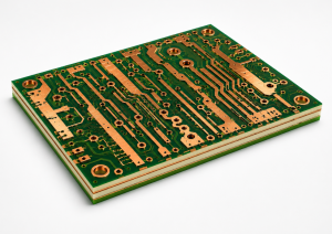
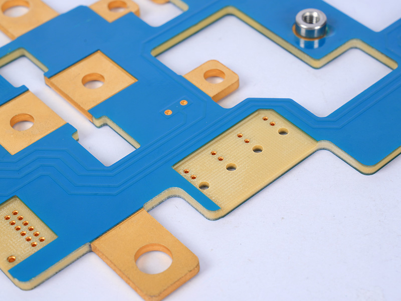
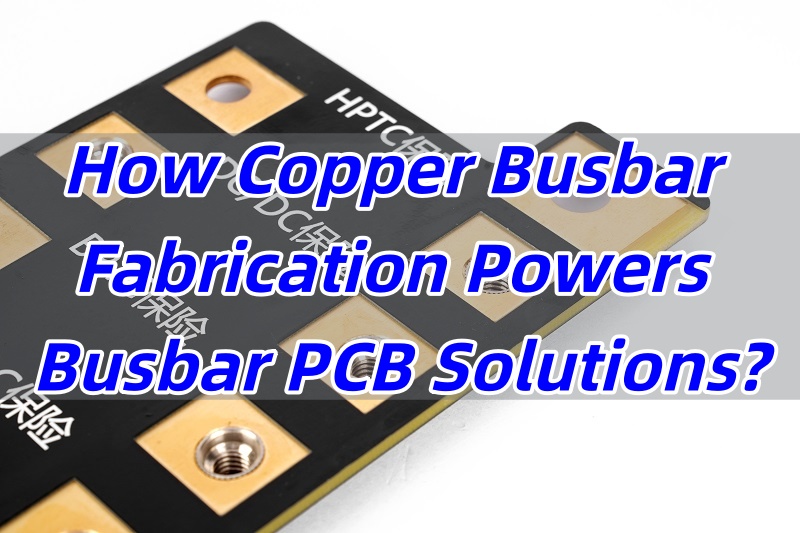
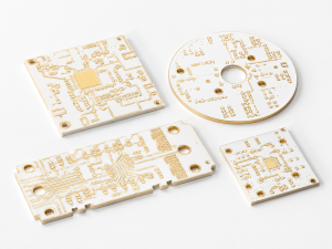
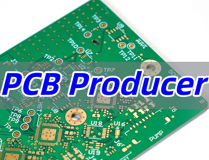
Why Choose EBest as Your Trusted Antenna PCB Manufacturer?
When it comes to Antenna PCB manufacturing, precision, reliability, and expertise are non-negotiable—and EBest stands out as the top choice for businesses across industries. Our end-to-end solutions for Antenna PCB design, prototyping, and assembly deliver consistent quality, fast turnaround, and customizations tailored to your unique requirements. Whether you’re in medical, aerospace, or industrial equipment sector, we have the technical capability to bring your Antenna PCB projects to life seamlessly.
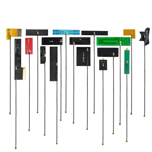
Users consistently seek clear, actionable answers about Antenna PCBs, focusing on practical applications and problem-solving. The most common searches revolve around design optimization, material selection, prototype reliability, and assembly quality—all areas where EBest excels. Below, we break down the core focus areas and how we address them, ensuring you get the insights and solutions you need for your Antenna PCB projects.
How to Optimize Antenna PCB Design for Maximum Performance?
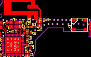
Antenna PCB design is the foundation of reliable wireless performance, and most users struggle to balance size, frequency, and efficiency. The key pain points include poor impedance matching, insufficient keep-out areas, incorrect material selection, and frequency drift—all of which lead to weak signals, reduced range, and project delays.
Common Antenna PCB Design Pain Points & EBest’s Solutions
- Pain Point 1: Impedance Mismatch – Mismatched impedance (often deviating from the standard 50Ω) causes signal reflection (VSWR > 2:1) and power waste. Solution: Our engineers use HFSS and CST 3D electromagnetic simulation tools to design π-type/T-type matching circuits, ensuring impedance deviation ≤ ±5% and VSWR < 1.5:1 for optimal signal transmission.
- Pain Point 2: Insufficient Keep-Out Area – Metal traces or components near the antenna disrupt signal radiation, reducing efficiency by 30% or more. Solution: We strictly adhere to keep-out area guidelines (≥ wavelength/4; e.g., ≥31mm for 2.4GHz Antenna PCBs) and ensure no copper cladding or vias are present in the antenna projection area to eliminate interference.
- Pain Point 3: Poor Material Selection – Using standard FR-4 for high-frequency applications (≥6GHz) leads to high signal loss (tanδ > 0.02) and unstable performance. Solution: We select materials based on your frequency needs—Rogers RO4350B (εr=3.48, tanδ=0.0037) for high-frequency Antenna PCBs, FR-4 for low-frequency, and ceramic substrates for GPS Antenna PCBs—to maximize efficiency (≥70% for 5G applications).
- Pain Point 4: Frequency Drift – Temperature fluctuations (-40℃~85℃) cause substrate expansion and contraction, shifting the resonant frequency. Solution: We conduct thermal cycling tests during design and optimize antenna dimensions to ensure frequency drift ≤ ±1% across industrial temperature ranges, guaranteeing stability in harsh environments.
For stress-free, high-performance Antenna PCB design for 2.4GHz, trust EBest’s engineering team. We translate your requirements into optimized designs that avoid common pitfalls—contact us today to start your custom Antenna PCB design project.
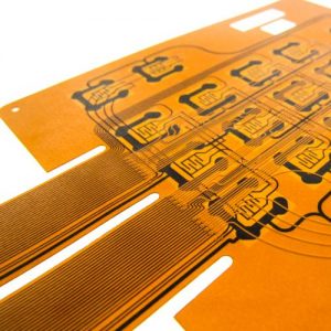
How to Get Reliable Antenna PCB Prototype Fast Without Compromising Quality?
Antenna PCB prototyping is critical for validating design performance, but users face two major pain points: slow turnaround times (10+ days) and inconsistent prototype quality that fails to reflect mass production performance. This leads to repeated iterations, increased project timelines, and missed deadlines—problems EBest solves with our streamlined prototyping process.
Antenna PCB Prototype Pain Points & EBest’s Solutions
- Pain Point 1: Slow Turnaround – Most manufacturers take 7-14 days to deliver Antenna PCB prototypes. Solution: Our in-house prototyping production line enables 2-3 day turnaround for standard Antenna PCB prototypes and 4-5 days for complex multi-layer (8+ layers) or high-frequency Antenna PCB prototype, without cutting corners on quality.
- Pain Point 2: Prototype-Production Mismatch – Prototypes made with different materials or processes than mass production fail to accurately test performance. Solution: We use the same materials, etching processes, and quality controls for prototypes as we do for mass production, ensuring your Antenna PCB prototype’s performance matches the final product exactly.
- Pain Point 3: Lack of Comprehensive Testing – Unverified prototypes lead to costly design flaws in production. Solution: Every Antenna PCB prototype undergoes rigorous testing—VNA (Vector Network Analyzer) for S11 parameters (target: <-10dB), OTA efficiency testing, and thermal shock testing—to validate signal performance, efficiency, and stability before you move to production.
Need a reliable, fast high-frequency Antenna PCB prototype to validate your design? EBest’s prototyping service delivers accurate, tested prototypes on time—let us help you avoid costly iterations and speed up your time to market.
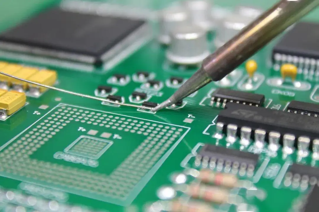
How to Ensure High-Quality Antenna PCB Assembly for Industrial & Medical Applications?
Antenna PCB assembly requires precise soldering, component placement, and shielding to maintain signal integrity—yet users often struggle with poor solder joints, component misalignment, and interference from nearby components. These issues are critical in medical and aerospace applications, where Antenna PCB failure can lead to safety risks and compliance violations.
Antenna PCB Assembly Pain Points & EBest’s Solutions
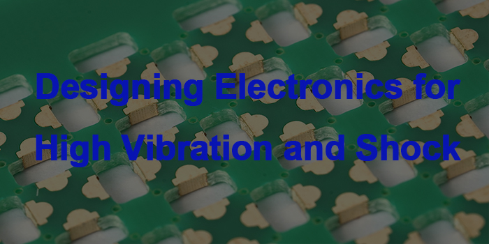
- Pain Point 1: Poor Solder Joints – Cold solder or bridging causes intermittent signal loss, especially in high-vibration environments (e.g., industrial equipment). Solution: We use automated SMT assembly with laser soldering for precision, and 100% AOI (Automated Optical Inspection) + X-ray inspection to detect and eliminate solder defects, ensuring joint reliability.
- Pain Point 2: Component Misalignment – Misplaced components (e.g., matching capacitors) disrupt impedance matching and signal performance. Solution: Our assembly line uses high-precision placement machines (±0.03mm accuracy) to ensure components are aligned perfectly with antenna traces, maintaining optimal performance.
- Pain Point 3: Electromagnetic Interference (EMI) – Nearby components or traces cause EMI, degrading Antenna PCB performance by 20%+ (critical for medical devices like remote patient monitors). Solution: We integrate EMI shielding for Antenna PCB (conductive coatings or metal enclosures) and optimize component placement to minimize interference, complying with ISO 13485 for medical applications.
- Pain Point 4: Compliance Failures – Aerospace and medical Antenna PCB assembly must meet strict industry standards (e.g., IPC-A-610, ISO 13485). Solution: Our assembly process is fully compliant with global standards, and we provide detailed inspection reports and certification documentation for every Medical Antenna PCB assembly order.
For high-quality, compliant Medical Antenna PCB assembly you can trust, EBest is your partner. We specialize in assembly for medical, aerospace, and industrial Antenna PCBs—contact us to discuss your assembly requirements.
What Are the Different Types of Antenna PCB for Industrial & Aerospace Use?
Choosing the right Antenna PCB type is critical for matching application requirements (frequency, size, gain). Below is a comparison of common Antenna PCB types, their uses, and EBest’s customization capabilities—helping you select the perfect solution for your project.
| Antenna PCB Type | Key Features | Industry Applications | EBest Customization |
|---|---|---|---|
| Microstrip Patch Antenna PCB | High directionality, gain 2-5dBi, compact size (30mm×25mm for 2.4GHz) | Aerospace (satellite communication), industrial IoT sensors | Custom patch size, multi-element arrays (8×8 for 77GHz radar) |
| PIFA Antenna PCB (Planar Inverted-F) | Low profile (<5mm), gain 3-6dBi, wide bandwidth (10-15%) | Medical (wearable health monitors), aerospace (cabin communication) | Short-circuit pin optimization, ultra-thin design for compact devices |
| Loop Antenna PCB | Anti-interference, gain 1-3dBi, small size (10-20mm diameter) | Industrial (asset tracking), medical (implantable devices) | Closed-loop design, custom diameter for low-frequency (433MHz/868MHz) use |
| Millimeter Wave Antenna PCB | High gain (15-20dBi), narrow beam, low loss | Aerospace (radar systems), industrial (high-precision monitoring) | Low-loss Rogers substrates, multi-array integration for high accuracy |
Antenna PCB Application Cases: Medical, Aerospace & Industrial
EBest has extensive experience delivering custom Antenna PCB solutions for mission-critical industries. Below are real-world cases showcasing our expertise in solving complex Antenna PCB challenges.
Medical Industry Case: Remote Patient Monitor Antenna PCB
A leading medical device manufacturer needed an Antenna PCB for a remote patient monitor (2.4GHz WiFi/Bluetooth) that met ISO 13485 standards, had low power consumption, and resisted EMI from hospital equipment. We designed a compact Custom PIFA Antenna PCB with a Rogers RO4350B substrate, integrated EMI shielding for Antenna PCB, and optimized impedance matching to ensure reliable signal transmission (range ≥50m) in hospital environments. The Antenna PCB passed all biocompatibility and EMI tests and is now used in 10,000+ monitors worldwide.
Aerospace Industry Case: Satellite Communication Antenna PCB
An aerospace client required a high-frequency (28GHz) Antenna PCB for satellite communication, with high gain (≥18dBi), low signal loss, and resistance to extreme temperatures (-55℃~125℃). We designed a millimeter wave antenna array PCB with 16×16 microstrip elements, using a Aerospace Antenna PCB substrate (Rogers 5880, tanδ=0.0009) for minimal loss. The Antenna PCB underwent vibration, thermal cycling, and radiation testing, meeting NASA’s aerospace standards, and is now integrated into small satellites for Earth observation.
Industrial Industry Case: Industrial Sensor Antenna PCB
An industrial automation company needed an Antenna PCB for a LoRa sensor (868MHz) used in factory asset tracking, requiring long range (≥1km) and resistance to vibration and dust. We designed a loop Antenna PCB with an FR-4 substrate, optimized for low-frequency performance and compact size (15mm diameter). The Antenna PCB was integrated into the sensor’s housing with IP67 protection and now provides reliable data transmission across 50+ factories, reducing downtime by 30%.
Why Choose EBest for Your Antenna PCB Needs?
When you partner with EBest for Antenna PCB design, prototyping, or assembly, you get the expertise, quality, and reliability that set us apart from other manufacturers. Here’s why we’re the top choice for businesses worldwide:
- Technical Expertise – Our team of RF engineers has 15+ years of experience in Antenna PCB design, specializing in high-frequency, medical, and aerospace applications.
- End-to-End Solutions – We handle every step from design, prototyping, and assembly to testing and delivery, eliminating the need for multiple vendors.
- Strict Quality Control – 100% inspection (AOI, X-ray, VNA) and compliance with IPC-A-610, ISO 9001, ISO 13485, and aerospace standards.
- Fast Turnaround – 2-3 day prototype delivery and 5-7 day mass production delivery for standard Antenna PCB orders.
- Customization – Tailored Antenna PCB solutions for any frequency (433MHz~60GHz), size, and industry requirement, including Custom PIFA Antenna PCB and Aerospace Antenna PCB substrate options.
- Proven Track Record – Trusted by 500+ clients in the medical, aerospace, and industrial sectors, with 99.8% on-time delivery and 99.5% customer satisfaction.
FAQ: Common Antenna PCB Questions & Answers
1. What substrate is best for high-frequency Antenna PCB?
For high-frequency Antenna PCBs (≥6GHz), low-loss substrates like Rogers RO4350B (εr=3.48, tanδ=0.0037) or Rogers 5880 (εr=2.2, tanδ=0.0009) are best. These substrates minimize signal loss, ensure impedance stability, and support high gain—critical for 5G and millimeter wave applications. Standard FR-4 is unsuitable for high frequencies due to high tanδ (>0.02) and signal degradation.
2. How do I reduce EMI in Antenna PCB assembly?
To reduce EMI shielding for Antenna PCB in assembly, use three key strategies: 1) Optimize component placement—keep high-noise components (e.g., power regulators) ≥20mm away from the antenna. 2) Add EMI shielding (conductive coatings or metal enclosures) around the antenna to block external interference. 3) Use grounded guard traces between the antenna and other traces to isolate signal paths. EBest implements all three in every Antenna PCB assembly for medical and industrial applications.
3. What is the ideal keep-out area for Antenna PCB?
The ideal keep-out area for an Antenna PCB is ≥ wavelength/4 of your operating frequency. For example: 2.4GHz (wavelength ≈124mm) requires a keep-out area of ≥31mm; 5GHz (wavelength ≈60mm) requires ≥15mm; 868MHz (wavelength ≈345mm) requires ≥86mm. This area must be free of copper cladding, vias, and components to avoid signal disruption and efficiency loss.
4. How long does it take to get an Antenna PCB prototype?
EBest delivers standard Antenna PCB prototypes in 2-3 days. Complex prototypes (multi-layer, high-frequency, or custom shapes) take 4-5 days. This fast turnaround is possible due to our in-house prototyping production line and streamlined design-to-production process, which eliminates delays from third-party vendors.
5. Can Antenna PCB be customized for small form-factor devices?
Yes, Antenna PCBs can be fully customized for small form-factor devices (e.g., wearables, IoT sensors, medical implants). EBest designs compact Antenna PCB types like Custom PIFA Antenna PCB (height <5mm) or snake-shaped traces to fit tight spaces while maintaining performance. We’ve designed Antenna PCBs as small as 5mm×5mm for wearable health monitors, without sacrificing signal range or efficiency.
6. What tests are required for medical Antenna PCB?
Medical Antenna PCBs require four key tests to meet ISO 13485 standards: 1) EMI/EMC testing to ensure compatibility with hospital equipment. 2) Thermal cycling testing (-40℃~85℃) to validate performance in varying environments. 3) Biocompatibility testing (if the Antenna PCB is in contact with skin or body fluids). 4) Signal performance testing (VNA, OTA efficiency) to ensure reliable data transmission. EBest provides full test reports for every Medical Antenna PCB assembly order.
Get Your Custom Antenna PCB Today – Contact EBest
We provide high-quality Antenna PCB design, prototyping, and assembly solutions, tailored to your industry and application needs. Whether you’re in the medical, aerospace, or industrial equipment sector, our team has the expertise to deliver reliable, compliant, and high-performance Antenna PCBs on time. For your next Antenna PCB project, contact us to place your order at sales@bestpcbs.com. EBest – Your Trusted Antenna PCB Partner.