

Can one loose socket in a hotswap PCB lead to PCB failure after assembly? For mechanical board projects, the answer is yes. A small socket issue, bent switch leg, weak solder joint, or wrong firmware file can cause unstable input, missed signals, or repair work later.
A hotswap PCB makes switch replacement easier because users do not need to solder every switch leg. However, it still needs proper socket design, pad strength, layout accuracy, USB stability, firmware matching, and final testing. This guide explains how to test, remove switches, build, repair, solder, and update firmware for a hotswap PCB in a practical way.
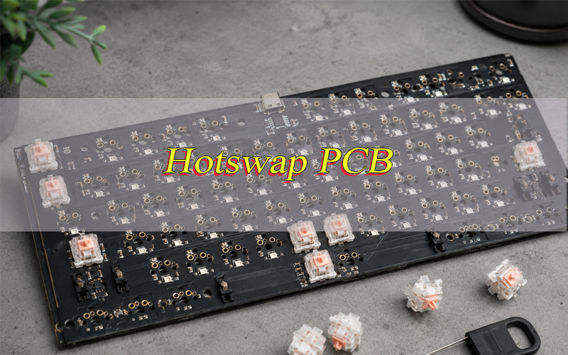
What Is a Hotswap PCB?
A hotswap PCB is a printed circuit board that allows mechanical switches to be installed and removed without soldering the switch legs directly to the board. Instead of fixed solder joints on every switch, the board uses small metal sockets soldered to the PCB pads.
When a switch is pressed into the socket, its metal legs touch the internal spring contacts inside the socket. This creates the electrical path needed for the controller to read the press.
This structure is useful when users want to try different switch types, repair a single switch site, or assemble a board without soldering tools. It is also helpful for product teams that need fast switch trials before final production.
A hotswap PCB still needs careful design. The socket footprint, copper pad size, solder joint strength, plate alignment, case clearance, USB circuit, diode layout, and firmware all affect the final result. A loose socket or misaligned plate can cause intermittent input even when the switch itself is good.
How Does a Hotswap PCB for Mechanical Boards Work?
A hotswap PCB works by using switch sockets as removable electrical connection points. The user presses a mechanical switch into the socket, and the socket connects the switch legs to the circuit.
- Switch legs enter the socket contacts. The two metal legs on the switch slide into the socket and touch the internal contacts.
- The socket is soldered to PCB pads. The socket itself is fixed to copper pads on the PCB by solder, so pad strength matters.
- The plate helps alignment. A plate above the PCB keeps switches straight and reduces side stress on the socket.
- The matrix circuit reads input. Rows and columns allow many switch sites to be scanned with fewer controller pins.
- Diodes help prevent ghosting. A diode near each switch site can help the board read multiple presses more accurately.
- The controller sends signals to the computer. The controller reads the matrix and sends input data through USB or wireless firmware.
- Firmware defines behavior. Firmware controls layers, lighting, rotary encoder actions, and switch assignments.
What Is the Difference Between Hotswap and Solder PCB?
Hotswap and solder PCB designs can both provide reliable input performance, but they serve different build styles. Hotswap focuses on fast switch changes and easier service, while solder PCB focuses on direct permanent switch joints.
| Item | Hotswap PCB | Solder PCB |
|---|---|---|
| Switch installation | Press switches into sockets | Solder switch legs to pads |
| Switch change | Fast and tool-light | Requires solder removal and rework |
| Assembly difficulty | Easier for many users | Requires soldering skill |
| Long-term joint style | Socket contact plus soldered socket pads | Direct solder joints on switch legs |
| Layout flexibility | Limited by socket footprint and plate fit | More flexible for some split layouts |
| Common repair area | Socket, pad, diode, USB, firmware | Solder joint, pad, diode, USB, firmware |
| Good use case | Switch trials, frequent switch changes, serviceable builds | Permanent builds, specialty layouts, firm switch mounting |
For a mechanical board that will be opened and modified often, a hotswap PCB is usually more convenient. For a special layout, ultra-firm build, or design where socket clearance is limited, a solder PCB may still be the better route.
What Layout Sizes Are Available for Hotswap PCB?
Hotswap PCB layouts are usually named by physical size and switch count. The right size depends on desk space, input habit, shortcut needs, and case design.
- 60 hotswap PCB: A compact layout with no separate F-row, arrow cluster, or number pad. It saves desk space and is common in portable mechanical boards.
- 65 percent hotswap PCB: Similar to 60 percent, but usually adds arrows and a small right-side cluster. It gives a practical balance between size and daily use.
- 75 hotswap PCB: Keeps the F-row, arrows, and navigation cluster in a tight format. It is popular for office work, coding, and daily writing.
- TKL hotswap PCB: Removes the number pad but keeps arrows and the F-row. It gives a classic feel with more desk space for a mouse.
- Full size hotswap PCB: Includes the number pad. It is useful for finance, data entry, office stations, and industrial input devices.
- Wired non flex cut hotswap PCB: A wired board without flex cuts. It often feels firmer and may offer a more consistent acoustic response than a heavily cut board.
Flex cuts can change input feel by adding board movement. A non flex cut design gives more rigidity, which some users prefer for a stable sound and firm switch feel.
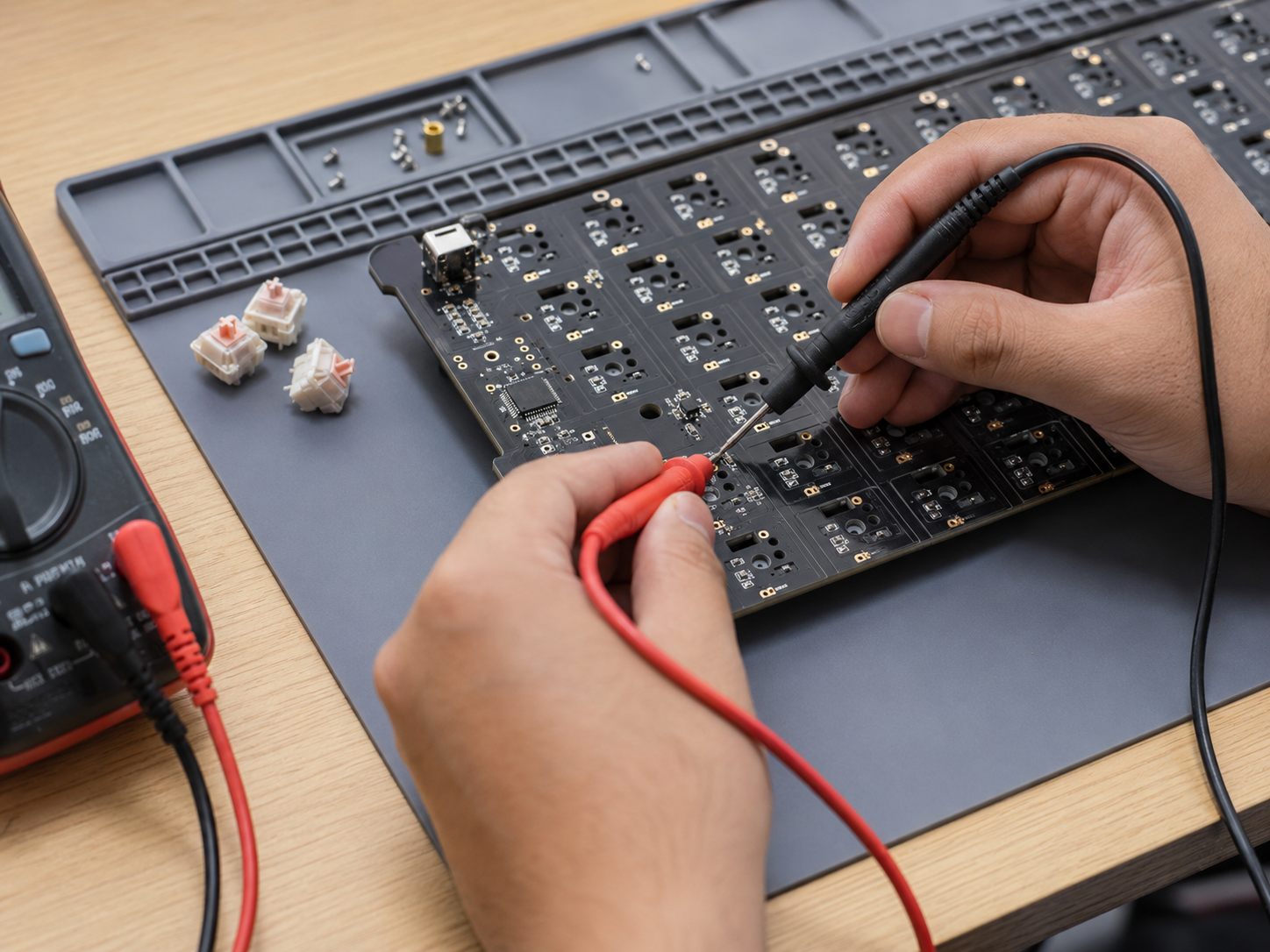
How to Test Hotswap PCB?
Testing a hotswap PCB before assembly helps find socket, diode, USB, and firmware problems early. A board may look clean, but one loose socket or wrong firmware file can still cause unstable input. It is better to test the bare PCB first, then test it again after switches and the case are installed.
- Inspect the PCB surface first.
Check for scratched traces, solder bridges, shifted sockets, missing diodes, damaged pads, and poor solder joints. Do not power the PCB if there is an obvious short-circuit risk. - Check every hotswap socket.
Each socket should sit flat on the PCB. If a socket is tilted, cracked, or lifted from the pads, the switch may not make stable contact. - Connect the PCB to a computer.
Use a known good USB cable. If the board is not detected, try another cable and USB port first. Then inspect the USB connector and nearby components. - Use a switch test tool.
Open VIA, Vial, QMK Toolbox, or another compatible test tool. Confirm that the board can be recognized correctly. - Short each switch position with tweezers.
Touch the two contacts of each socket with tweezers. If the correct signal appears, the circuit at that position is working. If there is no response, check the socket, diode, solder joint, and trace. - Check row and column faults.
If only one position fails, the issue is usually local. If several positions in the same row or column fail, inspect the matrix route, diode direction, or controller area. - Install switches and test again.
After the bare PCB test, install switches and press each position several times. If one switch works only at a certain angle, check the switch legs and socket contact. - Test after final assembly.
The PCB may pass before assembly but fail after being placed in the case. Plate pressure, screw tension, or case mismatch can affect socket alignment, so final testing is necessary. - Verify firmware behavior.
Test switch mapping, layers, lighting modes, and special functions. Wrong firmware can make a good PCB seem defective.
A proper hotswap PCB test should confirm USB detection, socket response, row and column function, firmware mapping, and final assembly stability.
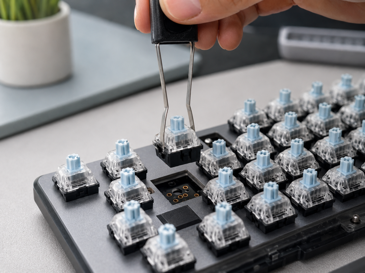
How to Remove Switch from Hotswap PCB?
Removing a switch from a hotswap PCB is simple, but the motion must be controlled. Side force can loosen the socket or bend the switch legs.
- Disconnect the cable first. Do not remove switches while the board is powered.
- Remove the top cap from the switch. This gives access to the switch housing.
- Use a proper switch puller. Grip the top and bottom latch points of the switch housing.
- Pull straight upward. Keep the force vertical so the switch legs leave the socket cleanly.
- Avoid twisting. Rocking the switch from side to side can stress the socket pads.
- Check the switch legs. Bent legs can miss the socket contacts during reinstallation.
- Inspect the socket. If the socket moves, lifts, or feels loose, the board needs repair before use.
- Install slowly. Align both switch legs with the socket openings before pressing down.
If a switch feels stuck, do not force it. Check whether the plate latch is holding the switch body too tightly. A tight plate can make removal harder than the socket itself.
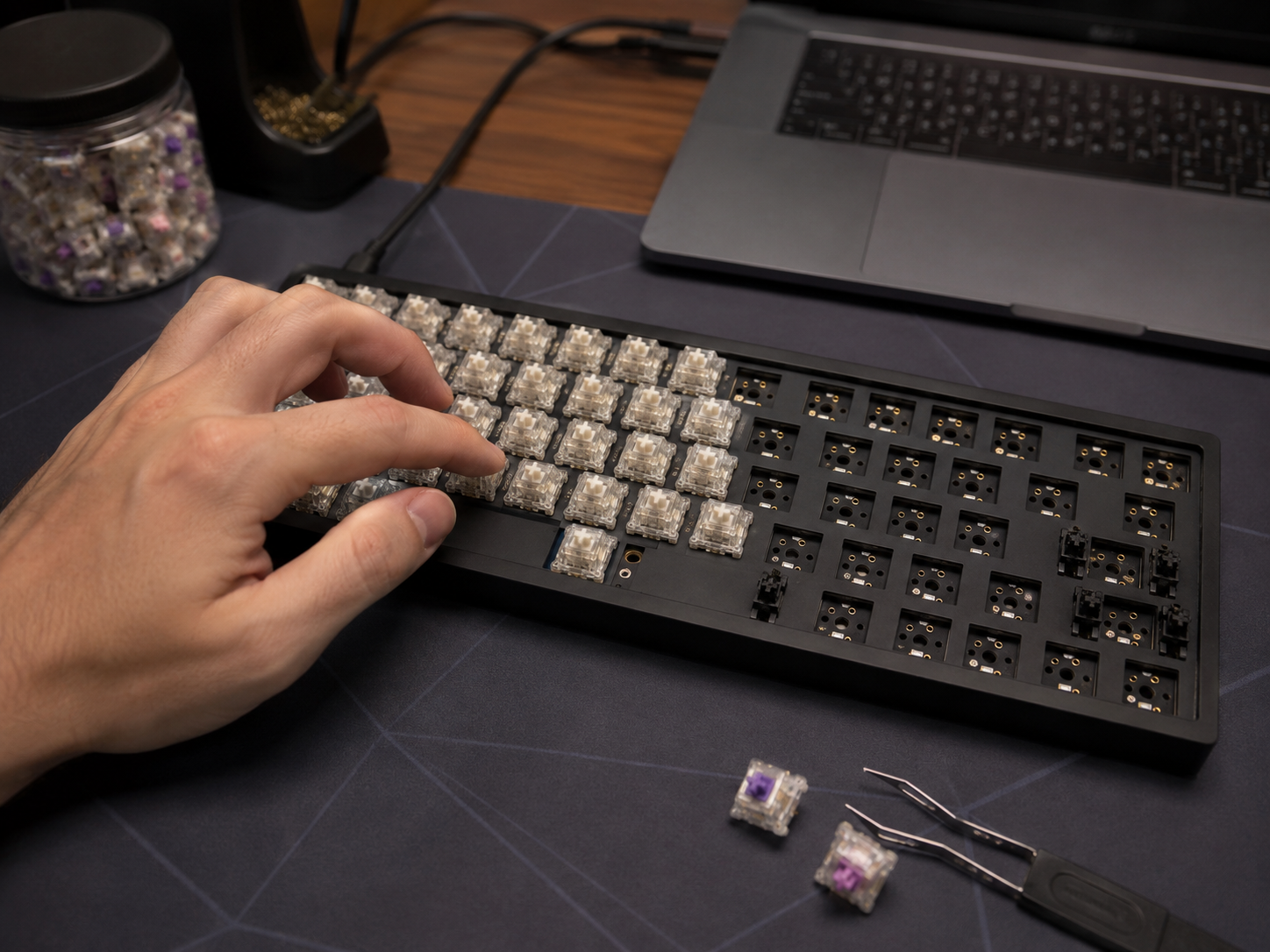
How to Make Hotswap PCB?
Making a hotswap PCB requires correct socket design, stable pad structure, accurate layout, and proper testing. It is not simply adding sockets to a normal PCB. The socket footprint, switch position, plate, case, and firmware must match from the beginning.
- Choose the layout.
Decide whether the PCB will be 60%, 65%, 75%, TKL, full size, or a custom layout. The layout affects switch count, PCB outline, mounting holes, and firmware mapping. - Confirm switch compatibility.
Most hotswap PCB designs use MX-style switches. The PCB should have the correct switch holes, socket positions, and stabilizer support for larger positions. - Use the correct hotswap socket footprint.
The socket footprint must match the socket model. Incorrect pad spacing can cause weak solder joints, poor contact, or difficult assembly. - Strengthen the socket pads.
Socket pads need enough copper support because they carry both electrical contact and mechanical stress. Weak pads can lift during switch removal. - Design the switch matrix.
Plan rows and columns clearly. Clean routing makes the PCB easier to test, repair, and produce. - Place diodes correctly.
Diodes should match the matrix design and firmware direction. Clear silkscreen markings help avoid assembly mistakes. - Design a stable USB-C area.
Use the correct connector footprint, strong anchor pads, ESD protection, and clean power routing. The USB area should be mechanically strong because it is used often. - Check plate and case alignment.
Switch legs must enter the sockets vertically. If the plate or case is misaligned, the switch may press the socket at an angle and damage the pads. - Choose a suitable surface finish.
ENIG is often used for this type of PCB because it provides a flat surface and good solderability. - Run DFM review before production.
Check pad size, solder mask opening, socket orientation, diode direction, trace spacing, mounting holes, and USB connector strength before fabrication. - Build and test a prototype.
A prototype helps confirm socket contact, switch fit, USB function, firmware mapping, and case assembly before batch production. - Prepare complete production files.
Provide Gerber files, drill files, BOM, placement file, surface finish requirement, firmware notes, and testing instructions.
A good hotswap PCB should be easy to assemble, stable during use, and durable enough for repeated switch changes. This depends on socket quality, pad strength, layout accuracy, and full testing.
How to Fix Hotswap PCB?
Fixing a hotswap PCB should start with careful checking, not immediate soldering. Many issues come from bent switch legs, loose sockets, damaged pads, diode faults, USB connection problems, or firmware mismatch. A step-by-step check can help you find the real cause before making the problem worse.
- Check the switch first.
If only one switch position does not respond, remove the switch and inspect both metal legs. Bent legs may fail to enter the socket correctly. Straighten the legs gently, reinstall the switch vertically, and test again. - Test the socket with tweezers.
After removing the switch, short the two socket contacts with tweezers. If the signal appears on the test tool, the PCB circuit is likely working, and the issue may come from the switch or poor contact. If there is still no response, continue checking the socket, diode, and circuit path. - Inspect the hotswap socket.
Look at the socket from the back side of the PCB. If it is loose, tilted, cracked, or partly lifted from the pads, the connection may be unstable. A loose socket usually needs proper rework instead of repeated switch insertion. - Check for lifted pads.
Repeated switch removal, side pressure, or rough handling can damage the copper pads under the socket. If the pad is lifted, simple resoldering may not fully restore the circuit. The damaged area may need jumper wire repair or pad reconstruction. - Inspect the diode near the failed position.
Many hotswap PCB designs use one diode for each switch position. If the diode is reversed, cracked, missing, or poorly soldered, that position may fail. Compare it with nearby positions to check its direction and solder condition. - Check row or column problems.
If several positions fail in the same row or column, the issue may come from the matrix circuit rather than a single socket. Inspect nearby traces, diodes, solder joints, and controller pins. This type of fault needs more systematic testing. - Examine the USB connector.
If the whole PCB is not detected by the computer, try another USB cable first. Then check whether the USB-C connector is loose, cracked, or poorly soldered. Also inspect the surrounding ESD protection parts and power path. - Confirm the firmware.
A firmware mismatch can cause wrong input, missing positions, lighting errors, or detection problems. Make sure the firmware file matches the exact PCB layout and controller. After flashing, test every switch position again. - Check case and plate pressure.
Sometimes the PCB works before assembly but fails after being mounted in the case. Over-tightened screws, a misaligned plate, or uneven case pressure can affect socket contact. Loosen the screws slightly and test again. - Avoid unnecessary rework.
Do not apply heat to the board before confirming the fault location. Excessive heat can damage pads, sockets, plastic parts, and nearby components. Rework should be done only after visual inspection and electrical testing point to a clear fault.
A hotswap PCB is usually repairable when the problem is found early. The safest method is to test the switch, socket, diode, matrix route, USB area, and firmware in order, instead of replacing parts randomly.
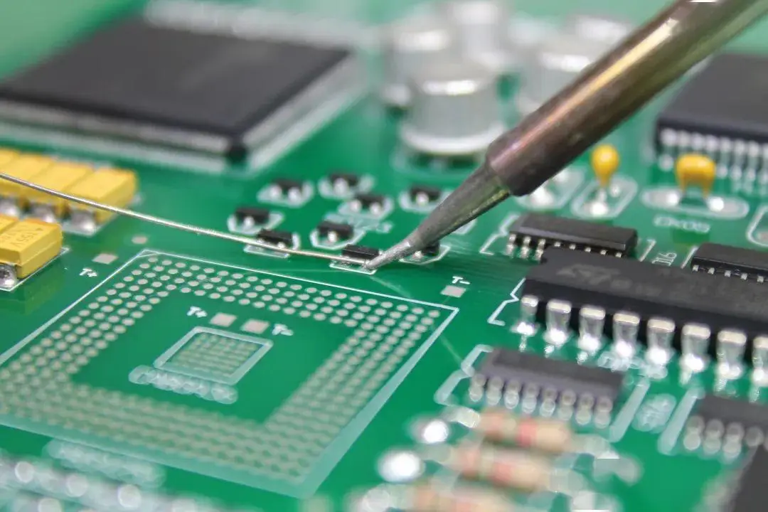
Can You Solder a Hotswap PCB?
Yes, you can solder a hotswap PCB, but you usually do not need to solder the switches. A hotswap PCB is designed with sockets, so the switch legs can plug into the socket contacts directly.
You can solder or rework the hotswap sockets if they become loose, cracked, or poorly connected. You may also repair nearby parts such as diodes, LEDs, resistors, reset buttons, or USB connectors when needed.
However, it is not recommended to solder switch legs directly into a hotswap socket area unless the PCB design clearly supports it. Direct soldering may damage the socket, lift copper pads, or make later switch removal difficult.
If repair is needed, remove old solder carefully, check whether the pad is still intact, align the socket correctly, and apply fresh solder with controlled heat. Too much heat can damage pads, sockets, and nearby components.
How to Change Firmware on Hotswap PCB?
Firmware changes are not defined by the socket type. A hotswap PCB can use VIA, Vial, QMK, a brand tool, or closed firmware depending on the controller and circuit design.
- Confirm firmware support. Check whether the PCB uses QMK, VIA, Vial, or a brand-specific tool.
- Get the correct firmware file. The file must match the exact board layout and controller.
- Save current settings. Export the current layout if the tool allows it.
- Enter bootloader mode. Use the reset button, reset pads, or a boot command based on the board design.
- Flash the firmware. Use QMK Toolbox, a web flasher, VIA-compatible tools, or the brand tool.
- Reconnect the board. Unplug and reconnect after flashing if required.
- Test every switch site. Confirm input, layers, lighting, encoder function, and macro behavior.
- Avoid mismatched firmware. Wrong firmware can cause missing input, wrong switch assignments, lighting errors, or USB detection problems.
Firmware work should be documented. Keep the firmware version, layout file, and test result together, especially when preparing a hotswap PCB for repeat production.
FAQs About Hotswap PCB
Q1: What is a wired non flex cut hotswap PCB?
A1: It is a wired hotswap PCB without flex cut slots. This design usually feels firmer because the board has less movement during input. It is suitable for users who prefer a stable feel and cleaner acoustic response.
Q2: Is a 60 hotswap PCB good for a small desk?
A2: Yes. A 60 hotswap PCB is a compact layout that saves desk space and leaves more room for mouse movement. It works well for minimal setups, but users who need arrows or an F-row may prefer 65 percent or 75 percent layouts.
Q3: Why is a 75 hotswap PCB popular?
A3: A 75 hotswap PCB is popular because it keeps the F-row, arrows, and navigation area in a compact body. It is a strong choice for writing, office work, programming, and daily input tasks.
Q4: Can a hotswap PCB use both 3-pin and 5-pin switches?
A4: It depends on the PCB hole design. A 5-pin compatible hotswap PCB can accept both 3-pin and 5-pin MX-style switches. A 3-pin-only board may require trimming the two plastic legs from a 5-pin switch.
Q5: Why does one switch site stop responding on a hotswap PCB?
A5: The common causes are a bent switch leg, loose socket contact, lifted pad, damaged diode, cracked solder joint, or firmware mismatch. Start with a tweezer test, then inspect the socket and diode before any rework.
Conclusion
A hotswap PCB gives mechanical board projects more flexibility, but stable performance depends on more than the socket itself. Pad strength, socket alignment, USB-C reliability, diode placement, firmware matching, surface finish, and final functional testing all affect the finished board.
Planning a custom hotswap PCB for a new product or batch build? EBest Circuit can support hotswap PCB fabrication(like FR4 PCB, HDI PCB and so on), socket assembly, USB-C PCB production, ENIG surface finish, DFM review, component sourcing, functional testing, and batch manufacturing. Send your Gerber files, BOM, layout notes, and test requirements to sales@bestpcbs.com. Our team will review your files and help you move from design check to reliable production with fewer hidden risks.
You may also like


Tags: 60 hotswap pcb, 75 hotswap pcb, Hotswap PCB keyboard, Hotswap PCB vs solder, wired non flex cut hotswap pcb