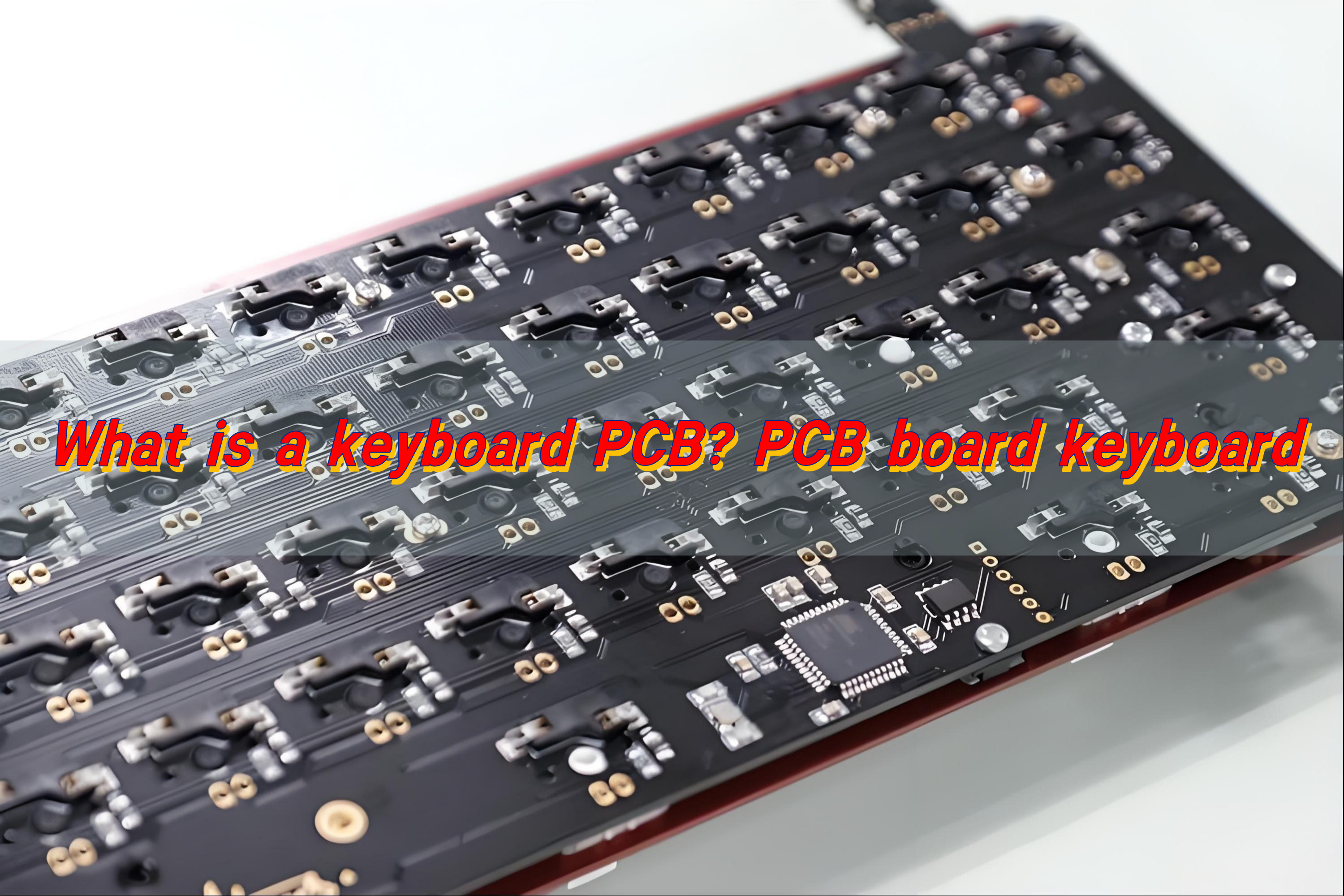
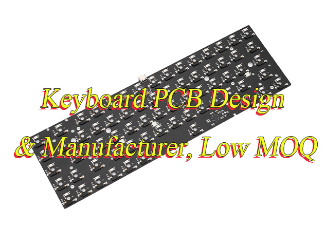
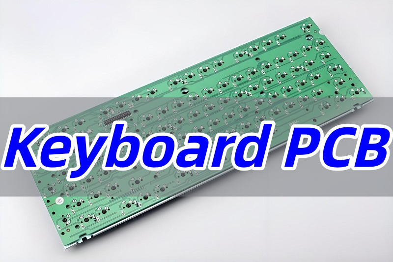
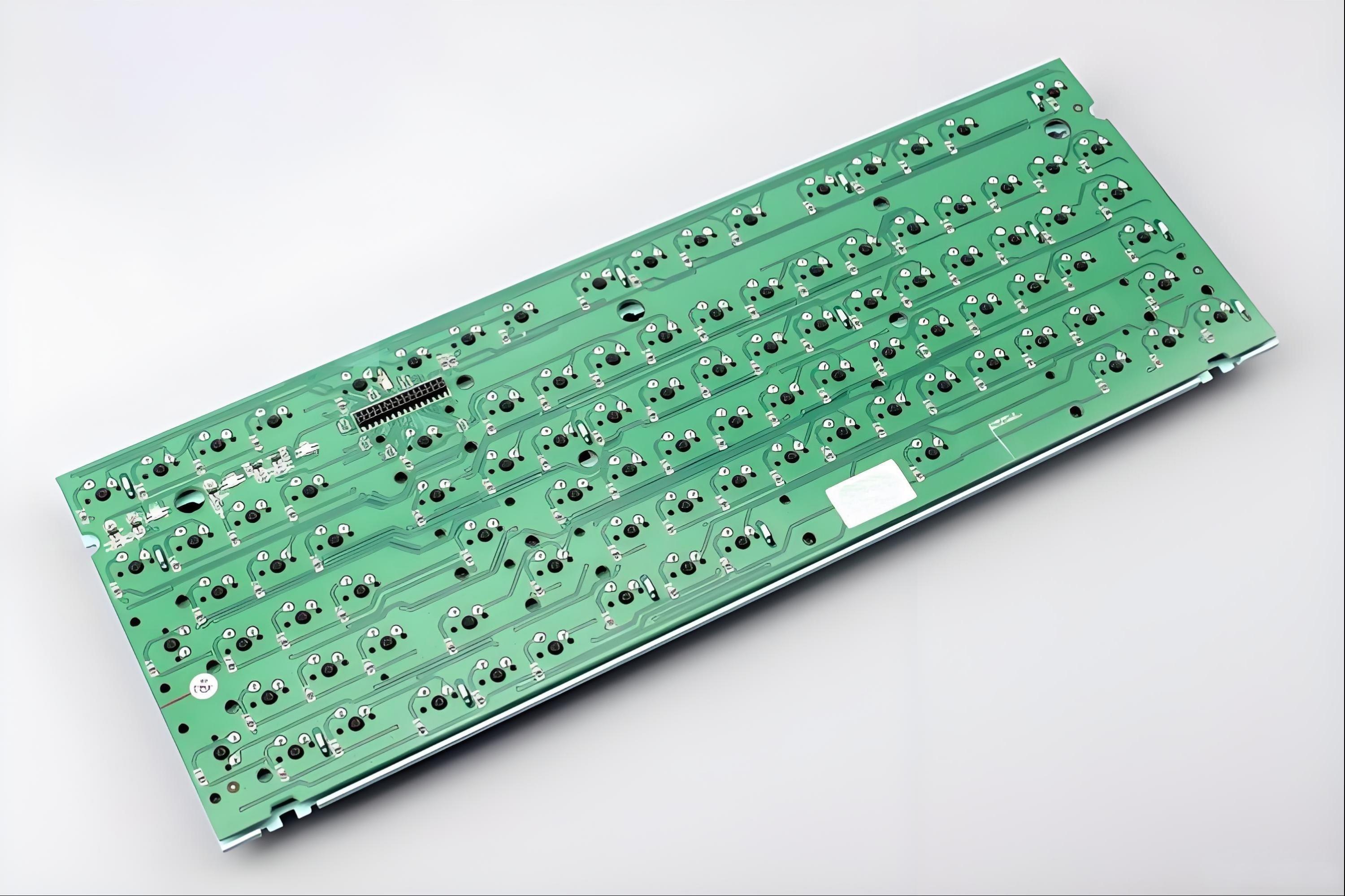
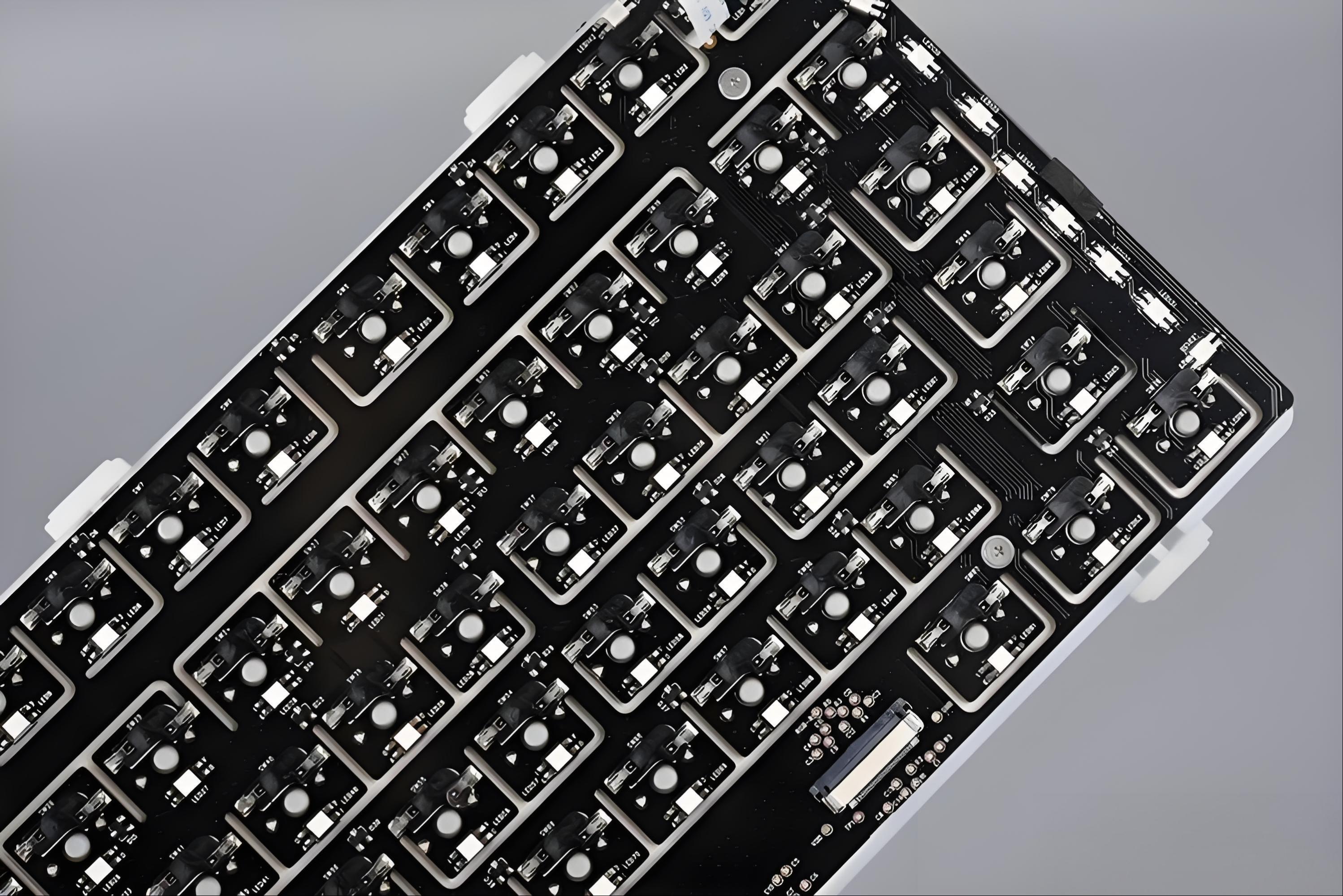
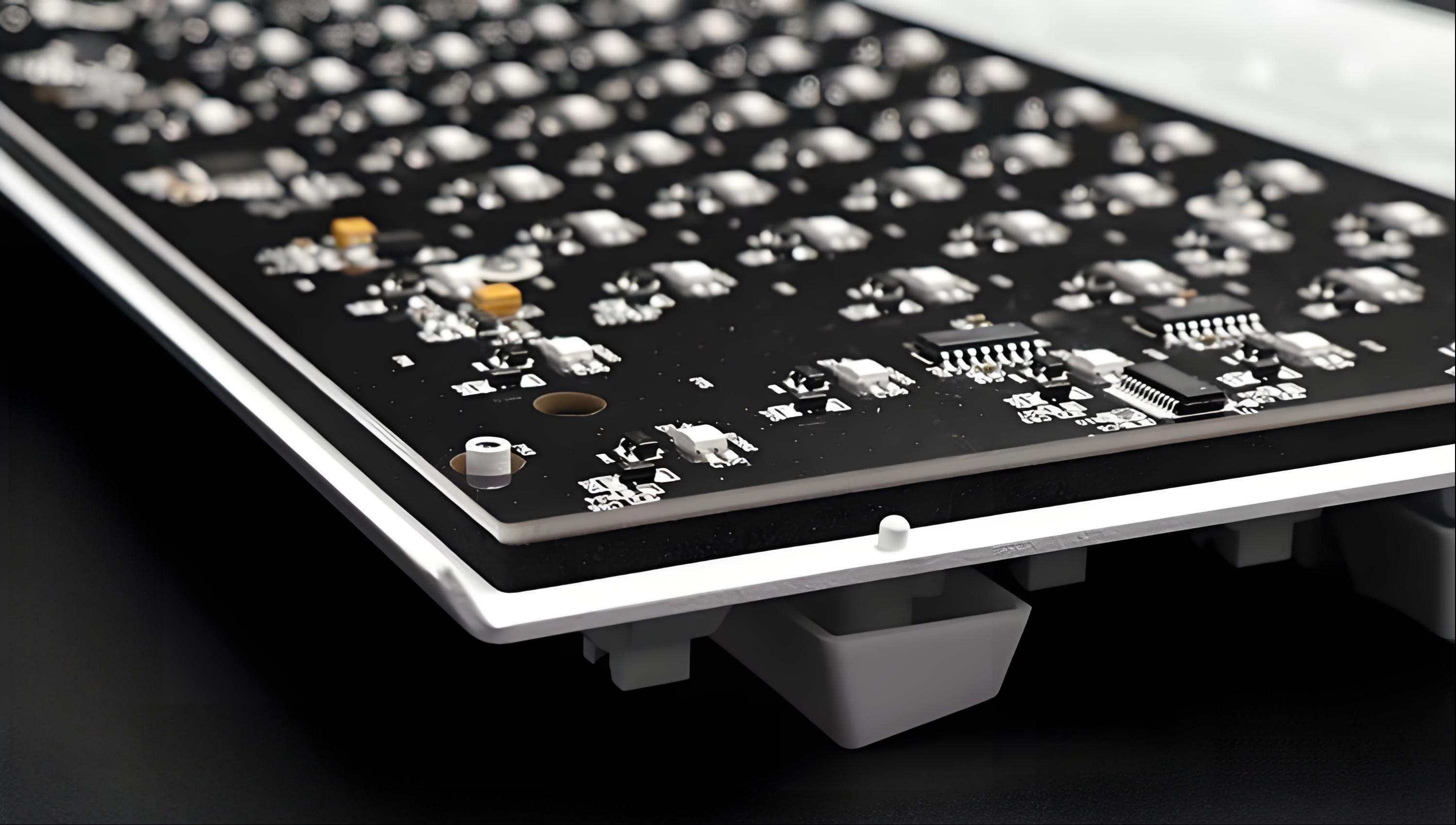
A keyboard PCB is the electrical core of a mechanical, magnetic, or custom keyboard. The keyboard PCB connects the switches or sensors to a microcontroller, processes each keypress, and sends the input to a computer or other host device.
Boards that share the same size label are not always interchangeable. Mounting holes, USB position, stabilizer support, switch orientation, case dimensions, firmware, and plate layout can all differ.
For a personal DIY build, an existing PCB may be sufficient. A commercial project needs a more disciplined review of the electrical design, mechanical fit, component supply, manufacturing files, firmware, and test process.
What Is a Keyboard PCB?
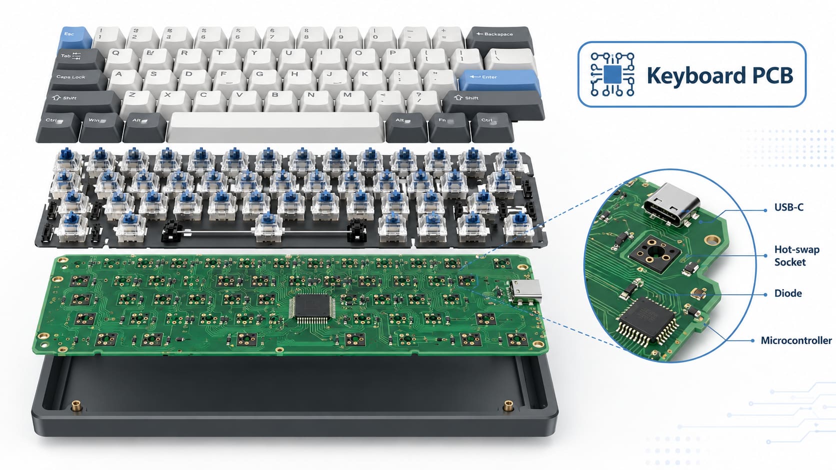
A keyboard PCB, or printed circuit board, connects the keys, controller, USB interface, LEDs, and other electronic functions.
In a standard mechanical keyboard, pressing a switch closes an electrical path. The microcontroller detects that change through a row-and-column matrix, identifies the key position, and sends the assigned keycode through USB or a wireless connection.
Depending on the product, the PCB may also include:
- Hot-swap sockets
- Per-key RGB LEDs
- Rotary encoders
- Displays
- Battery charging circuits
- Wireless modules
- Hall Effect or TMR sensors
The PCB affects more than basic key input. It also determines layout support, switch orientation, firmware compatibility, repairability, lighting position, and case fit.
How Does a Mechanical Keyboard PCB Work?
Most mechanical keyboard PCBs use a switch matrix instead of assigning one microcontroller pin to every key.
The switches are arranged into rows and columns. The controller scans these lines continuously. When a key closes a row-column connection, the firmware identifies the position and sends the corresponding keycode.
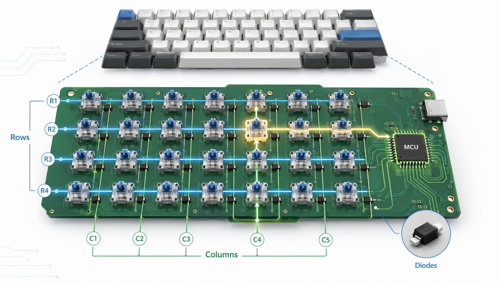
A 5-row by 15-column matrix can support up to 75 positions while using only 20 controller pins. This is far more practical than wiring each key independently.
A diode is normally placed in series with each switch. It controls current direction and reduces ghosting when several keys are pressed at the same time.
The operating sequence is straightforward:
- The controller scans the matrix.
- A switch closes a row-column connection.
- The firmware identifies the key position.
- Debouncing filters contact noise.
- The assigned keycode or macro is sent to the host.
Scan rate, debounce settings, firmware efficiency, and USB polling all influence response. A high advertised polling rate alone does not guarantee low end-to-end latency.
What Components Are Used on a Keyboard PCB?
The component set changes according to the switch technology, communication method, and product features.
| Component | Function | Key Design Check |
|---|---|---|
| Mechanical switch | Creates the key input | Confirm 3-pin, 5-pin, PCB-mount, or plate-mount support |
| Diode | Controls matrix current direction | Match orientation with the schematic and firmware |
| Microcontroller | Scans keys and runs firmware | Check GPIO count, memory, USB support, and availability |
| Hot-swap socket | Holds removable switches | Verify footprint, orientation, and solder-pad strength |
| USB connector | Carries power and data | Provide mechanical anchoring and ESD protection |
| RGB LED | Provides key or case lighting | Check package, current, and data direction |
| Reset or boot switch | Supports firmware flashing | Keep accessible after assembly |
| Encoder | Adds rotary or push input | Confirm footprint and firmware support |
| Magnetic sensor | Measures switch magnet movement | Requires accurate placement and calibration |
| Wireless module | Adds Bluetooth or RF communication | Maintain antenna clearance |
| Battery circuit | Powers wireless products | Include charging and protection functions |
Component packages should be confirmed before PCB layout is frozen. A replacement part may have a different pinout, pad size, height, or assembly process even when its electrical function appears similar.
What Are the Main Types of Keyboard PCBs?
Keyboard PCBs are commonly classified by switch installation, sensing technology, and physical structure.
| PCB Type | Main Feature | Suitable Application |
|---|---|---|
| Soldered mechanical PCB | Switches are soldered directly | Fixed layouts and cost-sensitive builds |
| Hot-swap PCB | Switches plug into sockets | Retail keyboards and frequent switch replacement |
| Hall Effect PCB | Hall sensors measure magnetic travel | Adjustable actuation and rapid-trigger keyboards |
| TMR keyboard PCB | TMR sensors detect magnetic movement | High-sensitivity magnetic input systems |
| Split keyboard PCB | Left and right keys use separate boards | Ergonomic keyboards |
| Wireless keyboard PCB | Includes radio and battery circuits | Portable products |
| Reversible PCB | One design can be used for both halves | Low-volume split keyboard projects |
These categories can overlap. A keyboard may be wireless, split, hot-swap, and RGB-enabled at the same time. Each added function increases routing density, power demand, firmware work, and test coverage.
Hot-Swap vs Soldered Keyboard PCB: Which Is Better?
Choose hot-swap when easy switch replacement matters. Choose soldered construction when lower cost, layout flexibility, or strong permanent connections are more important.
| Factor | Hot-Swap PCB | Soldered PCB |
|---|---|---|
| Switch replacement | No soldering required | Desoldering required |
| Assembly | Fast after sockets are installed | Every switch must be soldered |
| Layout flexibility | Usually limited to fixed socket positions | Easier to support several switch positions |
| Component cost | Higher | Lower |
| Common failure point | Socket or lifted pad | Solder joint |
| Best fit | Retail and serviceable keyboards | Fixed layouts and specialist builds |
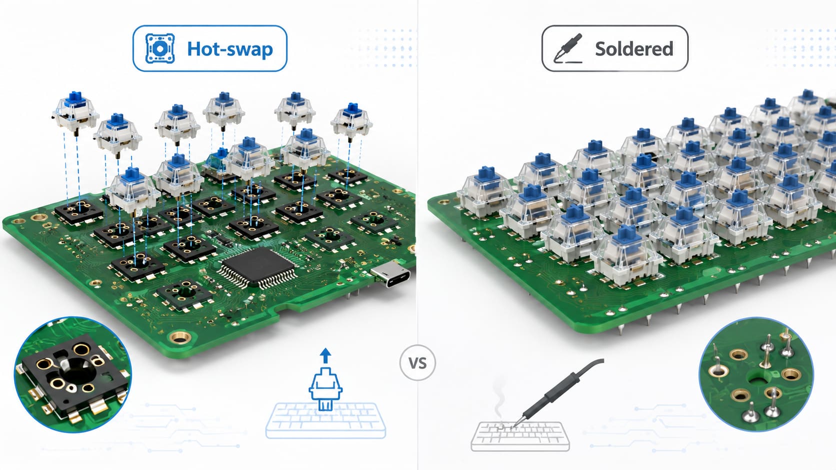
Hot-swap sockets are convenient but mechanically vulnerable. A bent switch pin can push against the socket, crack a solder joint, or lift a pad.
The plate should support the switches so insertion force is not transferred directly to the PCB. Commercial designs should be tested through repeated switch insertion and removal.
What Keyboard PCB Layout Should You Choose?
Keyboard percentages describe the general format, not a universal mechanical standard.
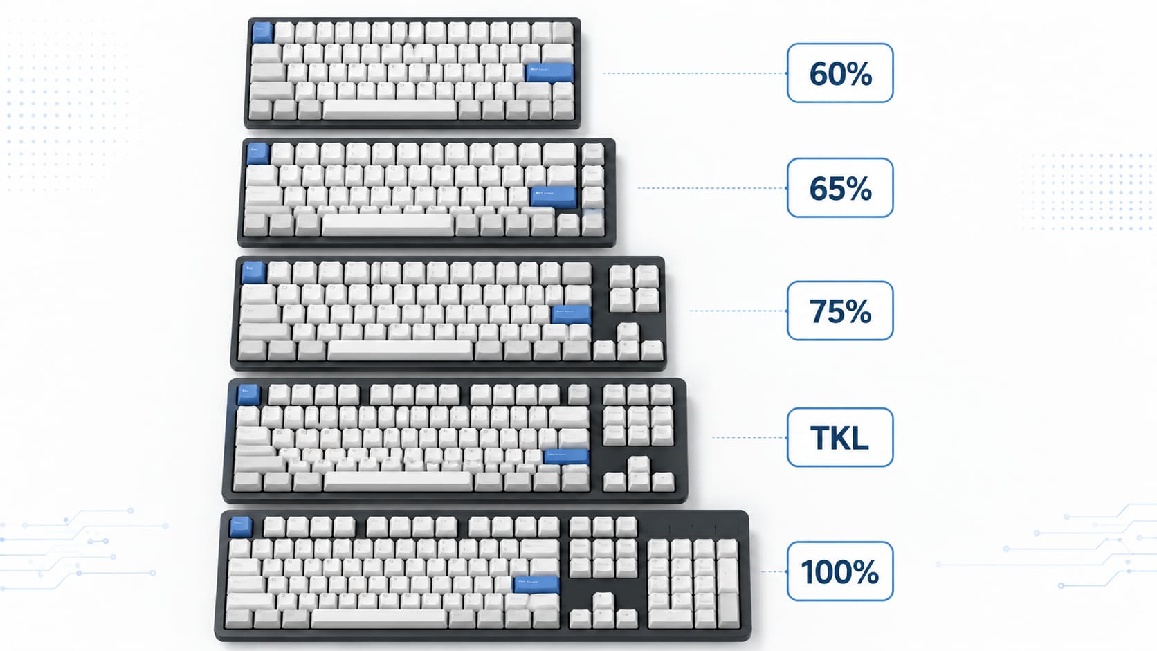
| Layout | Typical Configuration | Best Fit |
|---|---|---|
| 60% | No dedicated function row, arrows, or numpad | Compact builds |
| 65% | Adds arrow keys and limited navigation keys | Compact daily use |
| 75% | Includes function row in a compressed layout | Work and gaming |
| TKL | Full navigation area without numpad | General-purpose use |
| 96% or 1800 | Compact full-key layout with numpad | Data entry in less space |
| 100% | Full navigation cluster and numpad | Office and industrial use |
| Split | Separate left and right sections | Ergonomic keyboards |
Layout selection should be based on actual key requirements, not appearance alone. Confirm:
- Required key count
- ANSI, ISO, or JIS layout
- Dedicated function and navigation keys
- Numpad requirement
- Encoder or display position
- Stabilizer sizes
- Case width
- Firmware layer strategy
A smaller layout can recover missing functions through key layers, but that may not suit users who need frequent access to dedicated keys.
Are Keyboard PCBs Compatible with Every Case, Plate, and Switch?
No. A PCB is compatible only when its mechanical and electrical interfaces match the rest of the keyboard.
Check the following before purchasing or manufacturing:
- PCB outline: It must fit the case without touching walls, posts, batteries, or cables.
- Mounting holes: Hole positions must match the case structure.
- USB position: The connector must align with the case opening.
- Plate layout: Switch centers must match the plate cutouts.
- Stabilizers: Confirm screw-in, snap-in, PCB-mount, or plate-mount support.
- Bottom row: Spacebar and modifier sizes vary.
- Switch footprint: The PCB may support 3-pin, 5-pin, or both.
- Switch orientation: North-facing and south-facing layouts affect LED and keycap clearance.
- Daughterboard interface: Connector type and pinout must match.
- PCB thickness: Some sockets and connectors are designed around a specific board thickness.
A 60%, 65%, or 75% label is not enough to confirm fit. Mechanical drawings and mounting coordinates should be checked before ordering.
How Do You Design a Custom Keyboard PCB?
A custom keyboard PCB should be developed as an electrical, mechanical, firmware, and manufacturing system.
-
Define the product requirements
Confirm layout, switch technology, wired or wireless operation, lighting, display, encoder, battery, case size, production volume, and target cost.
-
Create the physical key layout
Set switch-center coordinates, key sizes, stabilizer positions, and optional bottom rows.
-
Choose the switch system
Decide between soldered switches, hot-swap sockets, low-profile switches, Hall Effect, or TMR sensing.
-
Build the matrix
Define row and column counts, diode direction, and controller pin assignments.
-
Select the microcontroller
Check GPIO count, USB support, memory, package, programming method, firmware support, and supply availability.
-
Complete the schematic
Include power, USB, reset, ESD, matrix, lighting, communication, and battery circuits where required.
-
Assign verified footprints
Compare every footprint with the component datasheet.
-
Import mechanical constraints
Add the PCB outline, mounting holes, case keep-outs, switch centers, and connector openings.
-
Place and route components
Prioritize USB signals, power distribution, sensor circuits, and connector access.
-
Run ERC and DRC
Resolve open nets, clearance violations, board-edge issues, and incorrect assignments.
-
Generate manufacturing files
Prepare Gerber, drill, BOM, CPL, assembly, programming, and test files according to the required service.
-
Build a complete prototype
Test the PCB inside the actual case with the plate, switches, firmware, and cables.
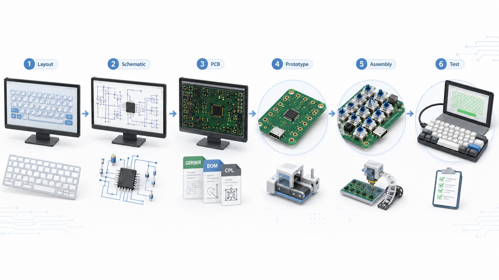
How Do You Create a Keyboard PCB Schematic?
Begin with the keyboard matrix. Assign every switch to a row and column, then place each diode in the chosen direction. The firmware matrix must use the same assignments.
The microcontroller section should include:
- Power and ground connections
- Decoupling capacitors
- Reset and boot controls
- Programming or debug access
- USB or communication pins
- Clock components where required
- Required pull-up or pull-down resistors
For USB-C, check the CC resistors, VBUS protection, ESD devices, connector shield strategy, and D+ and D− routing.
RGB circuits also need careful power planning. Confirm:
- LED supply voltage
- Maximum current
- Data-chain direction
- Bypass capacitors
- Power injection points
- Firmware brightness limits
Wireless keyboards need additional circuits for charging, battery protection, voltage regulation, power switching, and sleep control. Copper, batteries, and metal plates must stay clear of the antenna area.
Hall Effect and TMR designs require sensor power, filtering, signal acquisition, calibration support, and suitable controller inputs.
Which Tools Can Be Used for Keyboard PCB Design?
Different tools solve different parts of the design process.
| Tool | Main Use | Limitation |
|---|---|---|
| Keyboard Layout Editor | Defines key positions and sizes | Does not create a complete electrical design |
| Keyboard PCB generator | Creates initial placement or board files | Output still requires engineering review |
| Ergogen | Generates ergonomic and split layouts | Requires configuration and verification |
| KiCad | Schematic, PCB layout, DRC, and manufacturing output | Does not validate product compatibility by itself |
| QMK Configurator | Creates supported firmware configurations | Limited to compatible hardware |
| Mechanical CAD | Designs the case and plate | Does not handle electrical connectivity |
| Version control | Tracks PCB, firmware, and document changes | Requires consistent file management |
A common workflow starts with a layout editor, moves into KiCad for electrical design, and finishes with QMK or another firmware platform.
Generated libraries should be checked carefully. USB-C connectors, hot-swap sockets, low-profile switches, magnetic sensors, and encoders are common sources of footprint errors.
How Is a Hall Effect or TMR Keyboard PCB Different?
Hall Effect and TMR keyboards sense magnetic field changes instead of relying on metal contacts inside a mechanical switch.
A magnet moves with the switch stem. A sensor below the switch measures the magnetic change, allowing the controller to estimate travel position.
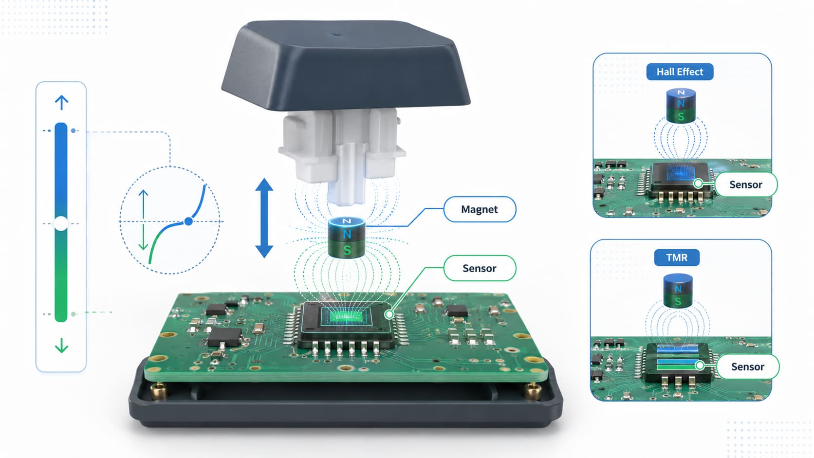
This supports features such as:
- Adjustable actuation
- Rapid trigger
- Multiple actions at different travel points
- Analog input
- Per-key calibration
Hall Effect and TMR are related but not identical.
| Factor | Hall Effect | TMR |
|---|---|---|
| Sensing method | Voltage response to magnetic field | Resistance change through magnetic tunnel junctions |
| Sensitivity | Suitable for most keyboard applications | Often higher |
| Power use | Device-dependent | Can be lower in suitable designs |
| Cost | Generally more established | May be higher |
| Design need | Alignment, filtering, and calibration | Alignment, calibration, and signal control |
| Switch compatibility | Requires matched magnet geometry | Requires matched magnet geometry |
A magnetic switch cannot be approved by external dimensions alone. Magnet polarity, strength, travel, sensor location, plate height, and wobble all affect performance.
A standard hot-swap mechanical PCB cannot normally be converted into a Hall Effect keyboard by replacing the switches. The board needs sensors, signal processing, compatible firmware, and a calibration process.
Production testing should measure sensor values at several travel positions. A basic pass-or-fail key test will not reveal inconsistent actuation points or poor sensor linearity.
What Should Be Considered When Designing a Split Keyboard PCB?
A split keyboard uses separate left and right sections that must exchange data and manage power safely.
Common architectures include:
- One controller with an I/O expander
- One controller on each half
- A wired master-secondary design
- Two wireless halves
The halves may connect through TRRS, USB-C, board-to-board cable, or wireless communication. A USB-C connector may carry a custom serial interface without operating as standard USB.
Important design checks include:
- Communication protocol
- Connector pinout
- Power direction
- ESD protection
- Reverse-voltage protection
- Hot-plug behavior
- Ground reference
- Firmware hand detection
- Battery arrangement
- Programming access
TRRS connectors need extra attention because the contacts can short briefly during insertion. The circuit should tolerate this, or the product documentation should prohibit powered hot-plugging.
A reversible PCB can reduce inventory for small projects, but it often complicates silkscreen, socket orientation, and assembly. Separate left and right boards are usually clearer for larger production runs.
What PCB Specifications Are Suitable for a Keyboard?
Most wired mechanical keyboards can use standard FR-4 materials and conventional PCB processes.
| Specification | Typical Starting Point | When to Upgrade |
|---|---|---|
| Layer count | 2-layer | Dense RGB, wireless, magnetic sensing, or limited routing space |
| Finished thickness | 1.6 mm | Low-profile, flex, or enclosure constraints |
| Copper weight | 1 oz | Higher current or special mechanical needs |
| Material | FR-4 | Higher reliability or dimensional stability requirements |
| Surface finish | Lead-free HASL or ENIG | Fine-pitch parts or flatter pad requirements |
| Via type | Through via | Blind or buried vias are rarely needed |
| Impedance control | Usually unnecessary for matrix signals | USB, radio, or defined high-speed interfaces |
| Electrical test | 100% bare-board test | Always followed by assembled functional testing |
A 2-layer PCB is sufficient for many wired keyboards. A 4-layer board may be worthwhile when the design includes wireless communication, dense per-key RGB, several power rails, or sensitive magnetic-sensor signals.
Flex cuts can soften the typing feel, but they reduce mechanical support. Avoid placing hot-swap pads, USB connectors, or narrow copper paths close to high-strain areas.
Decorative solder mask, exposed copper, and edge finishes should be listed separately during quotation so their real cost impact is clear.
What Files Are Required to Manufacture a Custom Keyboard PCB?
Bare PCB fabrication and PCBA assembly require different file packages.
| File or Information | Bare PCB | PCBA |
|---|---|---|
| Gerber files | Required | Required |
| NC drill files | Required | Required |
| PCB specification | Required | Required |
| Fabrication drawing | Recommended | Recommended |
| BOM | Not required | Required |
| CPL or pick-and-place file | Not required | Required |
| Assembly drawing | Not required | Recommended |
| Firmware file | Not required | Required if programming is requested |
| Programming instructions | Not required | Required if programming is requested |
| Test procedure | Not required | Required for functional testing |
| Mechanical drawing | Recommended | Recommended |
The BOM should include:
- Manufacturer part number
- Description
- Package
- Quantity
- Reference designators
- Approved alternatives
Descriptions such as “USB connector” or “RGB LED” are not specific enough for purchasing.
The CPL file must use the same origin and reference designators as the BOM and Gerber data. Rotation should be checked with an assembly drawing, especially for diodes, LEDs, sockets, connectors, sensors, and microcontrollers.
For quotation, also provide:
- Prototype and production quantities
- Required delivery date
- Bare PCB or full PCBA scope
- Customer-supplied components
- Programming requirements
- Test coverage
- Packaging requirements
A complete quotation package reduces assumptions and makes supplier comparisons more meaningful.
How Should a Keyboard PCB Be Tested Before Assembly?
Testing should move from bare-board inspection to full product validation.
-
Visual inspection
Check the outline, solder mask, silkscreen, USB position, switch footprints, and mounting holes.
-
Bare-board electrical test
Confirm open and short circuits through the PCB manufacturer’s electrical test process.
-
Resistance check
Measure resistance between power and ground before applying power.
-
Current-limited power-up
Verify rail voltages and check for abnormal heating.
-
Firmware flashing
Confirm bootloader access, USB enumeration, reset, and programming.
-
Matrix test
Test every key position and several multi-key combinations.
-
Hot-swap socket test
Inspect socket alignment and confirm stable contact with real switches.
-
Peripheral test
Verify RGB, encoders, displays, indicators, and optional interfaces.
-
Wireless test
Check pairing, charging, sleep current, wake behavior, and antenna performance.
-
Magnetic sensor calibration
Measure actuation, release, rapid-trigger response, and key-to-key variation.
-
Mechanical fit test
Assemble the board with the case, plate, stabilizers, battery, daughterboard, and cables.
-
Final functional test
Verify every key and feature using a defined test procedure.
A loose PCB test cannot reveal plate misalignment, blocked antennas, cable compression, or case interference. Final approval should be based on a fully assembled keyboard.
How Best Technology Supports Custom Keyboard PCB Projects
EBest Circuit, operated by Best Technology, supports keyboard PCB prototypes and assembled PCBA production.
Engineering review may include:
- Gerber and drill-file consistency
- Board outline and mounting-hole checks
- Trace, spacing, and annular-ring review
- Hot-swap socket footprint verification
- USB-C connector manufacturability
- Component orientation
- BOM availability
- Panelization
- Firmware programming instructions
- Functional-test requirements
Assembly services can include SMT placement, through-hole soldering, hot-swap socket assembly, RGB LED installation, MCU programming, AOI, X-ray inspection where appropriate, and customer-defined functional testing.
Customers should still provide the final case, plate, firmware, and compatibility requirements. Our PCB manufacturing capabilities support manufacturability review, but product-level fit and operating behavior must be validated against the actual keyboard design.
FAQs
1. What does PCB mean in a keyboard?
PCB means printed circuit board. It connects the switches or sensors to the controller and carries power, data, lighting, and control signals.
2. Can I design my own keyboard PCB with KiCad?
Yes. KiCad can be used for schematic design, footprint assignment, PCB routing, design-rule checks, and manufacturing output. You still need verified component libraries, a mechanical layout, and compatible firmware.
3. Are all 60%, 65%, and 75% keyboard PCBs interchangeable?
No. Boards with the same size label may use different outlines, mounting holes, USB positions, stabilizers, bottom rows, and plate structures.
4. Can Hall Effect switches be installed on a standard mechanical keyboard PCB?
Usually not. Hall Effect switches require magnetic sensors, compatible placement, signal-processing circuits, calibration, and dedicated firmware.
5. What files should I send for a custom keyboard PCB quotation?
For a bare PCB, send Gerber files, drill files, PCB specifications, quantity, and panel requirements. For PCBA, also provide the BOM, CPL file, assembly drawing, programming instructions, and test procedure.
A reliable keyboard project depends on matching the PCB with the switch system, case, plate, firmware, and production method. Standard mechanical designs are relatively straightforward. Wireless, split, hot-swap, Hall Effect, and TMR keyboards need more detailed compatibility and test planning.
For keyboard PCB fabrication, PCBA assembly, prototype review, or quotation support, contact EBest Circuit at sales@bestpcbs.com.