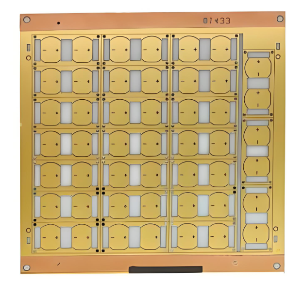
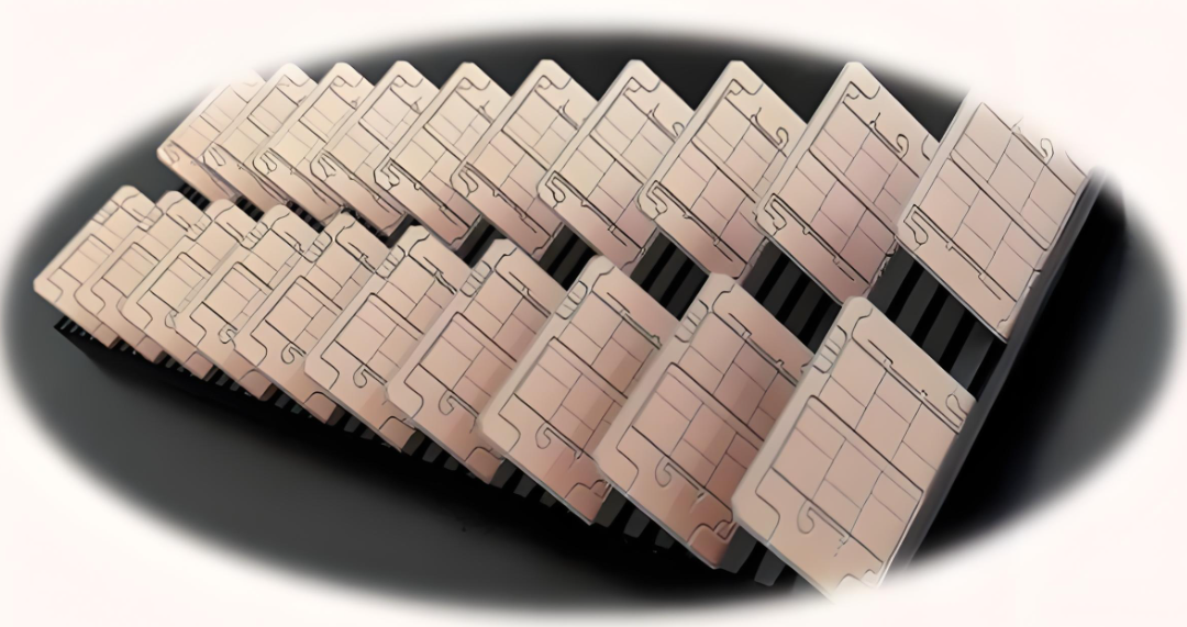
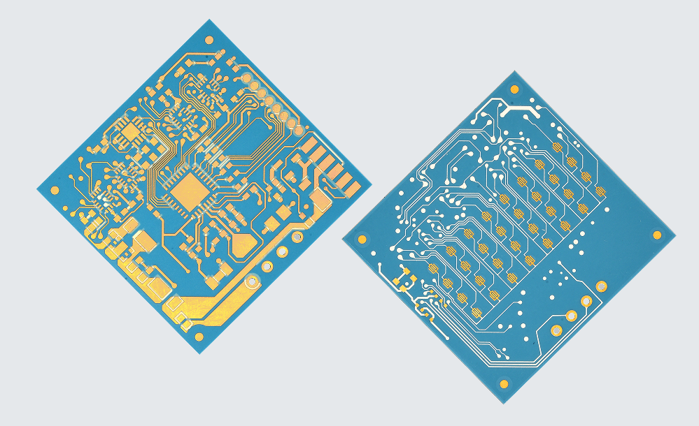
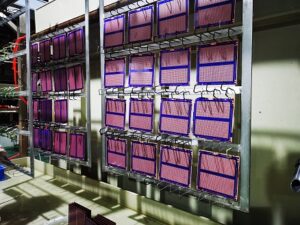
PCB manufacturing PCB manufacturing
Home > Blog

AMB Ceramic PCB

April 1st, 2026

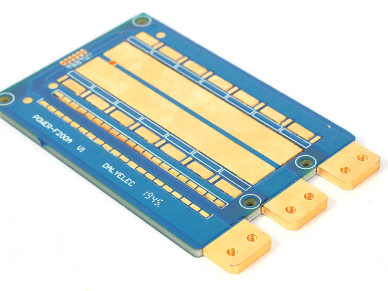
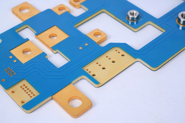
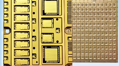
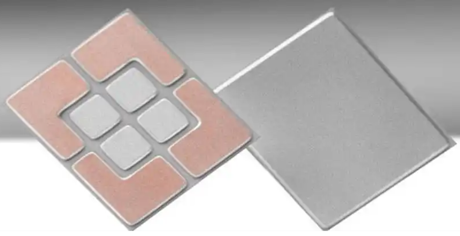
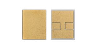
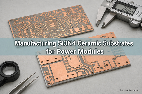
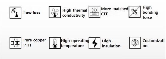
AMB Ceramic PCB is a high-performance ceramic substrate designed for power electronics that demand strong copper-to-ceramic bonding, efficient heat dissipation, and long-term reliability. At Best Technology, we provide custom AMB ceramic PCB solutions using Al2O3, AlN, and Si3N4 ceramic materials for customers in automotive, industrial, energy, rail transit, and high-power semiconductor industries.

If your project requires a substrate that can handle high current, thermal cycling, and harsh operating conditions, AMB PCB is a dependable choice.

Why Choose Best Technology for AMB Ceramic PCB?

At Best Technology (EBest Circuit), we provide advanced ceramic PCB solutions tailored for high-performance applications.

Our Strengths

  • 20+ years of PCB and PCBA experience
  • Support for Al2O3, AlN, and Si3N4 substrates
  • Copper thickness up to 800 µm
  • Strong expertise in power modules and thermal design
  • Full turnkey service from PCB to assembly
  • Certified with ISO 9001, ISO 13485, and IATF 16949

We work closely with engineers to optimize designs for manufacturability, reliability, and cost efficiency.

AMB Ceramic PCB

What Is AMB Ceramic PCB?

AMB stands for Active Metal Brazing. It is a ceramic substrate technology that bonds copper foil to ceramic by using active brazing materials containing metal elements such as titanium, silver, zirconium, or copper.

Unlike standard bonding methods, AMB creates a strong chemical bond between metal and ceramic at high temperature. This gives the finished substrate:

  • Higher bonding strength
  • Better resistance to thermal stress
  • Excellent heat transfer performance
  • Higher reliability in demanding environments

AMB ceramic PCB is widely used in power modules, IGBT modules, SiC packaging, EV systems, traction inverters, and renewable energy equipment.

Why Choose AMB Ceramic PCB?

For many power electronics projects, the substrate must do more than just carry traces. It must also help control heat, maintain insulation, and survive repeated thermal cycling. AMB ceramic PCB is chosen because it offers:

  • Stronger Bonding Performance

The active metal brazing process creates a reliable bond between copper and ceramic, making the substrate more suitable for high-power module packaging.

  • Better Reliability Under Thermal Stress

AMB substrates are designed for applications with frequent temperature changes and high operating loads. In advanced module structures, they can support very high thermal shock resistance.

  • Excellent Heat Dissipation

With the right ceramic material, AMB PCB can provide strong thermal performance for power semiconductors, converters, and high-current designs.

  • Good Match for Advanced Power Devices

AMB substrates are widely used with SiC chips, silver sintering processes, and thick copper designs, where both heat and reliability matter.

AMB Ceramic PCB vs DBC Ceramic PCB

Both AMB and DBC are used in ceramic substrate manufacturing, but they are not the same.

ItemDBC Ceramic PCBAMB Ceramic PCB
Bonding methodDirect bonding of copper to ceramicActive metal brazing
Process structureSimplerMore complex
Bonding strengthGoodHigher in many demanding applications
Thermal cycling reliabilityGoodExcellent
Suitable for harsh environmentsYesBetter suited for severe conditions
Typical high-reliability useStandard power modulesEV, traction, SiC, high-reliability power modules

In short, DBC is a strong option for many standard power applications, while AMB is often preferred when stronger bonding and better long-term reliability are required.

Ceramic Materials Available for AMB PCB

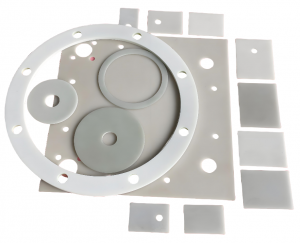
We provide AMB ceramic substrates based on different ceramic materials to match different power levels, cost targets, and reliability requirements.

1. Alumina AMB Ceramic PCB

Alumina is the most mature and cost-effective option.

Advantages:

  • Lower material cost
  • Stable supply
  • Mature manufacturing route
  • Good electrical insulation

Best for:

  • Cost-sensitive projects
  • Medium-power applications
  • Products with moderate thermal requirements

2. Aluminum Nitride AMB Ceramic PCB

AlN offers very high thermal conductivity, making it ideal for fast heat transfer.

Advantages:

  • High thermal conductivity
  • Excellent heat spreading
  • Suitable for high-power devices

Best for:

  • High-current applications
  • Power conversion systems
  • Compact designs with high heat density

3. Silicon Nitride AMB Ceramic PCB

Si3N4 is the preferred material for projects that require both mechanical reliability and thermal performance.

Advantages:

  • High bending strength
  • Strong thermal shock resistance
  • Thermal expansion closer to silicon
  • Excellent reliability in demanding environments

Best for:

  • Automotive power modules
  • Traction systems
  • Wind power converters
  • High-reliability SiC and IGBT packaging

Material Property Comparison

ItemUnitAl2O3AlNSi3N4
Densityg/cm³3.73.33.22
Thermal conductivityW/(m·K)>20>170>80
Coefficient of thermal expansionppm/°C6.94.72.5
Bending strengthMPa>350>350>700
Dielectric constant@1MHz9.89.08.0
Breakdown strengthkV/mm>15>20>20

Alumina AMB Ceramic PCB

Alumina ceramic PCB is the most mature and cost-effective option among AMB substrate materials.

Because alumina is widely available and easier to process, it is often used where budget control matters. The manufacturing base for alumina is also more established, which helps keep cost lower.

Advantages of Alumina AMB Substrates

  • Mature production process
  • Lower material cost
  • Stable electrical insulation
  • Good availability for volume production

Limitations of Alumina

The main limitation is its relatively low thermal conductivity. Compared with AlN and Si3N4, alumina transfers heat less efficiently. For that reason, it is more suitable for:

  • Low to medium power applications
  • Products with lower thermal load
  • Systems with moderate reliability requirements

Aluminum Nitride AMB Ceramic PCB

Aluminum nitride ceramic PCB is known for its very high thermal conductivity. This makes it a strong option for electronic products that need fast heat removal. With thermal conductivity above 170 W/(m·K), AlN performs much better than alumina in heat dissipation. It is often selected for:

  • High-power electronic devices
  • High-current modules
  • Power conversion systems
  • Applications with limited space for heat spreading

Benefits of AlN AMB Substrates

  • Excellent thermal conductivity
  • Strong electrical insulation
  • Good performance in high-power designs
  • Better thermal management than alumina

Design Consideration

Although AlN performs very well thermally, its mechanical toughness is not as strong as silicon nitride. In repeated high and low temperature cycling, this can limit its service life in some harsh environments.

So while AlN is a very capable choice, it is usually best for applications where heat transfer is the top priority, but extreme mechanical shock resistance is not the main concern.

Aluminum Nitride AMB Ceramic PCB

Silicon Nitride AMB Ceramic PCB

Silicon nitride ceramic PCB is often considered the premium choice for AMB applications that require both thermal performance and mechanical reliability.

Silicon nitride has a thermal conductivity above 90 W/(m·K) and a coefficient of thermal expansion very close to silicon. This helps reduce stress between the substrate and semiconductor chip during temperature changes.

It also offers very high bending strength, often above 700 MPa, which is much higher than alumina and AlN.

Why Si3N4 Stands Out

  • High mechanical strength
  • Good thermal conductivity
  • Excellent thermal shock resistance
  • Strong resistance to corrosion and oxidation
  • Better long-term reliability in harsh environments

High thermal conductivity silicon nitride ceramics usually contain a large proportion of the stable β-Si3N4 phase, which contributes to stronger and more reliable performance.

Typical Applications of Si3N4 AMB PCB

  • Automotive power modules
  • Wind turbine converters
  • Traction systems
  • High-voltage DC transmission
  • Power modules with partial discharge resistance requirements

In many advanced power systems, Si3N4 AMB substrates are selected when reliability matters just as much as heat dissipation.

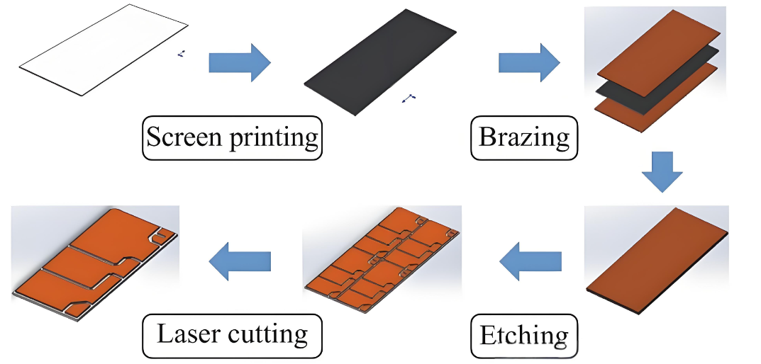
Main Manufacturing Process of AMB Ceramic PCB

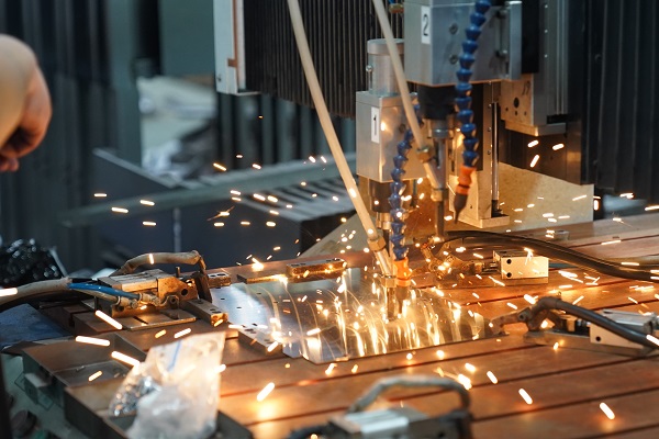
The manufacturing process of AMB ceramic PCB is more complex than standard PCB production because it combines ceramic processing, metal brazing, and precision patterning.

A typical AMB PCB production flow includes the following steps:

Main Manufacturing Process of AMB Ceramic PCB

1. Ceramic substrate preparation

The ceramic sheet is cleaned and prepared for bonding.

2. Active metal brazing paste or filler application

A brazing material containing active metal elements is applied evenly to the ceramic surface.

3. Copper foil alignment

Copper foil is placed on the ceramic substrate.

4. High-temperature brazing

The assembly is heated under controlled conditions so the active metal reacts with the ceramic and forms a strong bond.

5. Cooling and bond stabilization

The bonded structure is cooled carefully to maintain flatness and bond quality.

6. Circuit pattern imaging

The copper layer is patterned according to the circuit design.

7. Etching

Copper is etched, and in AMB structures the extra solder layer may also need to be removed.

8. Surface finishing and inspection

The finished substrate goes through surface treatment, dimensional inspection, and reliability checks.

Because AMB products include an additional brazing layer, the production route is more demanding than DBC. However, this extra process is also what enables AMB to achieve stronger bonding and better reliability in many power module applications.

Main Features of AMB PCB

  • High bonding strength between copper and ceramic
  • Excellent thermal dissipation for high-power devices
  • Strong thermal cycling reliability
  • Good compatibility with SiC and other advanced semiconductors
  • Stable electrical insulation under demanding conditions
  • High mechanical durability, especially with silicon nitride
  • Support for thick copper layers, in some cases up to 800 μm
  • Suitable for high-voltage and high-current applications

Common Applications of AMB Ceramic PCB

  • High-power semiconductor modules
  • High-frequency switching devices
  • Wind power systems
  • Solar energy equipment
  • Automotive electronics
  • Locomotives and rail transportation
  • Aerospace electronics
  • IGBT modules
  • 5G communication electronics
  • Medical devices
  • High-power LED lighting
  • Industrial control equipment
  • Defense and security systems

These applications often require a substrate that can operate under heat, vibration, current stress, and repeated thermal cycling without early failure.

Need a Reliable AMB Ceramic PCB Supplier?

If you are looking for an AMB ceramic PCB manufacturer for automotive, IGBT, SiC, renewable energy, or industrial power applications, Best Technology is ready to support your project.

Send us your design files or technical requirements, and our engineering team will review them and provide a suitable solution.

Email: sales@bestpcbs.com

You may also like

LTCC Ceramic PCB

April 1st, 2026

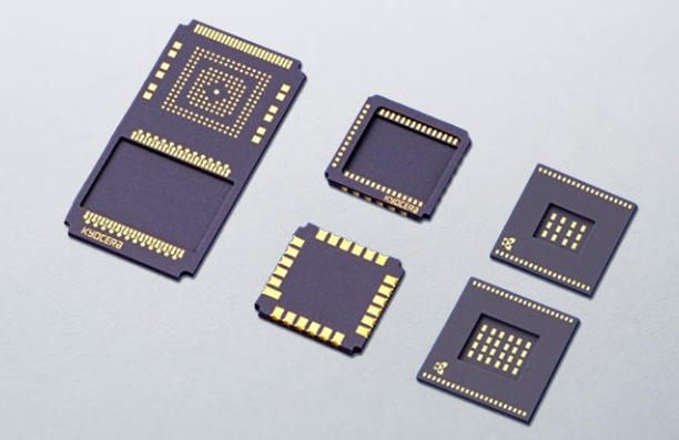
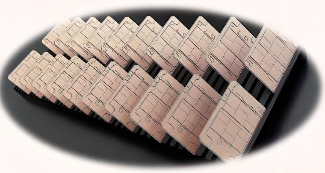
LTCC ceramic PCB is a multilayer ceramic substrate designed for compact, high-frequency, and high-reliability electronic applications. Best Technology provides custom LTCC ceramic solutions for RF modules, antennas, automotive electronics, communication devices, radar systems, and other advanced products.

Whether you need a compact multilayer ceramic substrate, embedded passive integration, or a stable platform for microwave and RF performance, our engineering team can support your project from design review to manufacturing.

What Is LTCC Ceramic PCB?

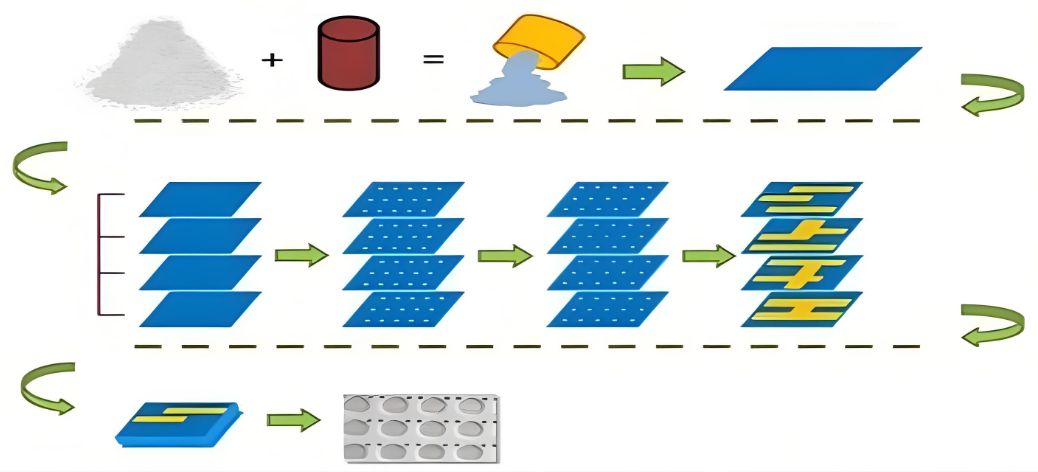
LTCC stands for Low Temperature Co-Fired Ceramic. It is made by printing conductive patterns on ceramic green sheets, stacking them layer by layer, filling vias, and co-firing the full structure at a relatively low temperature compared with traditional ceramic firing methods.

This process creates a dense and integrated ceramic substrate with excellent dimensional stability, good high-frequency performance, and strong suitability for miniaturized electronic modules.

Compared with conventional PCB materials, LTCC offers a more advanced packaging platform for applications that require smaller size, better electrical consistency, multilayer routing in limited space, embedded passive components, stable RF behavior, and reliable performance under temperature variation.

LTCC Ceramic PCB

LTCC Ceramic PCB

Why Choose LTCC Ceramic PCB?

LTCC is widely used when standard PCB materials are no longer enough for the design target. It helps engineers combine electrical performance, compact layout, and functional integration in one substrate.

Key Benefits of LTCC Ceramic PCB

  • High wiring density for multilayer compact designs
  • Embedded passive components to save board space
  • Good RF and microwave performance for signal-sensitive products
  • Low thermal expansion for better dimensional stability
  • Fine line capability for miniaturized circuits
  • Strong integration potential for compact modules
  • Reliable multilayer structure after co-firing
  • Better thermal behavior than many traditional PCB platforms

For products where size, signal quality, and long-term reliability matter, LTCC is often a strong engineering choice.

LTCC Ceramic PCB Features

Our LTCC ceramic substrates are designed for advanced electronic assemblies that need both performance and packaging efficiency.

LTCC Ceramic PCB Features

Multilayer Ceramic Structure

LTCC supports multilayer circuit construction in a compact body. This makes it suitable for products where design space is limited but routing demand is high.

Embedded Passive Integration

Passive elements such as resistors, capacitors, and inductive structures can be integrated into the substrate. This reduces surface crowding and leaves more space for active components.

Good High-Frequency Performance

LTCC is well suited for RF and microwave circuits because it supports short signal paths and effective grounding structures. This is especially valuable in antenna modules, filters, duplexers, and RF front-end designs.

Stable Performance Across Temperature Changes

Ceramic materials offer good thermal and dimensional stability. This helps maintain consistent electrical performance in demanding working environments.

Compact and Lightweight Design Support

By moving more functions into the substrate itself, LTCC helps reduce overall module size and supports lightweight electronic packaging.

LTCC Ceramic PCB Manufacturing Process

LTCC production is a controlled multilayer ceramic process. Each step directly affects the reliability and final performance of the substrate.

LTCC Ceramic PCB Manufacturing Process

1. Ceramic Slurry Preparation Ceramic powder, glass materials, and organic binders are mixed into a stable slurry.

2. Tape Casting The slurry is cast into thin ceramic green tapes with controlled thickness.

3. Via Punching Via holes are formed in the green sheets to create vertical electrical connections between layers.

4. Via Filling The vias are filled with conductive material to ensure interlayer conductivity after firing.

5. Circuit Printing Conductive pastes and functional materials are printed onto the ceramic sheets.

6. Layer Stacking and Alignment Each printed sheet is stacked in the required sequence with precise alignment.

7. Lamination The stacked structure is laminated under pressure to build a stable green body.

8. Co-Firing The laminated ceramic body is fired at around 850°C to 900°C, forming a dense integrated ceramic substrate.

9. Inspection and Testing Finished LTCC parts go through electrical and process inspection to verify quality and function.

Typical Applications of LTCC Ceramic PCB

LTCC is widely used in industries that demand compact structure, stable electrical performance, and reliable multilayer ceramic technology.

  • RF front-end modules
  • Antennas
  • Filters and duplexers
  • Automotive electronics
  • Radar systems
  • Aerospace electronics
  • Power base stations
  • Communication equipment
  • Microwave devices
  • Industrial electronic modules
  • High-density sensor packages
  • Compact wireless devices

As devices move toward higher frequency and smaller form factors, LTCC continues to be a preferred option for many advanced electronic designs.

LTCC Ceramic PCB for RF and Microwave Applications

LTCC is especially valuable in RF and microwave products because of its structural and electrical advantages.

For high-frequency circuits, shorter signal paths and strong grounding are essential. LTCC makes both easier to achieve in a compact footprint. It also supports integrated module design, which helps reduce assembly complexity and improve overall package efficiency.

This is why LTCC is often used in RF filters, antenna modules, duplexers, amplifier modules, integrated front-end modules, and high-frequency communication products.

For engineers working on compact RF systems, LTCC provides a practical balance of electrical performance and package miniaturization.

LTCC Ceramic PCB vs Traditional PCB

ItemLTCC Ceramic PCBTraditional PCB
Base MaterialCeramicOrganic laminate
StructureMultilayer co-fired ceramicLayered laminate board
Embedded PassivesAvailableLimited
High-Frequency SuitabilityExcellentDepends on material
Thermal StabilityHighModerate
Size Reduction PotentialStrongMore limited
Integration LevelHighLower
Dimensional StabilityStrongLower than ceramic

LTCC is not a replacement for every board type, but it is a better fit when the design requires high integration, compact size, and stable RF performance.

Custom LTCC Ceramic PCB Services

At Best Technology, we support custom LTCC ceramic substrate projects for a wide range of industrial and electronic applications.

  • Custom LTCC structure design
  • Engineering review before production
  • Via and multilayer layout support
  • Embedded passive integration discussion
  • Prototype and volume production support
  • Electrical performance-focused process control
  • Application-oriented technical communication

If your project requires a small ceramic module with reliable electrical performance, our team can help evaluate the right LTCC solution for your design.

Why Work With EBest Circuit (Best Technology)?

Choosing the right LTCC supplier is not only about price. It is also about process control, engineering support, and manufacturing consistency.

  • 20+ years of PCB and PCBA manufacturing experience
  • Support for ceramic PCB, MCPCB, FR4 PCB, and special PCB projects
  • Engineering-based communication for custom applications
  • Fast response for technical review and quotation
  • Support from prototype to mass production
  • One-stop service for PCB fabrication and assembly needs
  • Experience serving customers in industrial, automotive, and high-performance electronics fields

We understand that advanced ceramic substrates require more than standard production capability. They require close engineering coordination, controlled manufacturing steps, and clear communication throughout the project.

FAQ

What is LTCC ceramic PCB?

LTCC ceramic PCB is a low temperature co-fired ceramic substrate made by stacking printed ceramic green sheets and firing them into one multilayer ceramic structure.

What is the firing temperature of LTCC?

LTCC is typically co-fired at around 850°C to 900°C.

Why is LTCC used in RF applications?

LTCC supports compact multilayer designs, short signal paths, and strong grounding performance, which makes it suitable for RF and microwave modules.

Can LTCC include embedded passive components?

Yes. LTCC technology can integrate passive components inside the ceramic substrate, helping save surface space.

What industries use LTCC ceramic substrates?

LTCC is widely used in communication, automotive, aerospace, radar, industrial electronics, and high-frequency electronic products.

Is LTCC better than FR4?

It depends on the application. For standard electronics, FR4 may be enough. For compact RF modules, ceramic stability, and high integration needs, LTCC is often the better option.

Request a Quote for LTCC Ceramic PCB

Looking for a reliable LTCC ceramic PCB manufacturer for your next RF, microwave, or compact electronic project?

Best Technology provides custom ceramic PCB support based on your design and application needs. Send us your Gerber files, drawings, or technical requirements, and our team will review your project and provide a suitable solution.

Email: sales@bestpcbs.com

You may also like

Multi-Layer SinkPAD Board

March 31st, 2026

What Is a Multi-Layer SinkPAD Board?

A multi-layer SinkPAD board is a metal core PCB with more than two copper trace layers and a direct thermal path structure. The metal core is usually copper, and the thermal pad of the LED or power device is placed directly on the copper pedestal or copper core area. This allows heat to transfer quickly away from the component while the electrical circuits remain isolated through the dielectric layer.

Compared with a 1 layer SinkPAD board or a 2 layer SinkPAD board, the multi-layer version offers more routing space for complex circuits. The additional trace layers can be built on a single side or distributed on both sides of the board, depending on the product design.

Because of this structure, multi-layer SinkPAD boards combine two important functions in one compact platform: high-density circuit routing and efficient heat dissipation.

Multi-Layer SinkPAD Board

How Does a Multi-Layer SinkPAD Board Work?

The working principle of a multi-layer SinkPAD board is based on thermoelectric separation. The electrical current travels through the copper circuit layers, while the heat generated by the LED or semiconductor is transferred directly into the copper base through the thermal pad.

Since copper has very high thermal conductivity, around 400 W/m.K, heat can spread rapidly from the source to the metal base, and then into a heatsink, mounting surface, or surrounding air. This direct thermal path reduces thermal resistance and helps maintain lower operating temperatures.

At the same time, the extra routing layers allow engineers to build more sophisticated circuits in the same board area. This is useful when a product requires denser interconnections, control circuits, or more compact mechanical dimensions.

What Is the Difference Between Standard MCPCB and Multi-Layer SinkPAD Board?

A standard metal core PCB usually includes a dielectric layer between the heat source and the metal base. This provides insulation, but it also adds thermal resistance. In contrast, a multi-layer SinkPAD board uses a direct thermal path design, where the thermal pad of the LED or power device touches the copper core directly.

This difference offers several performance advantages:

  • Lower thermal resistance
  • Faster heat transfer
  • Better thermal stability for high-power devices
  • Higher routing density than basic SinkPAD boards
  • More flexibility for compact and complex circuit design

For designs that require both thermal efficiency and advanced routing capability, a multi-layer SinkPAD board is often a stronger choice than a conventional MCPCB.

Common Structures of Multi-Layer SinkPAD Board

4 Layer SinkPAD Board on the Same Side

One common structure is the 4 layer SinkPAD board with four trace layers built on the same side of the copper base. This design allows engineers to place more traces in the same board size and create more complex layouts than with a 1 layer or 2 layer SinkPAD board.

This structure is useful when the design needs strong thermal performance but also requires increased circuit density on one side.

Common Structures of Multi-Layer SinkPAD Board

Double-Sided 4 Layer SinkPAD Board

Another option is the double-sided 4 layer SinkPAD board, where two trace layers are placed on the top side and two trace layers are placed on the bottom side. This structure increases usable routing area and supports more advanced product architectures.

However, this type of board is more difficult to design and manufacture. Since components may be mounted on both sides, engineers must carefully consider how heat will be transferred to the heatsink.

Common Structures of Multi-Layer SinkPAD Board

Design Considerations for Double-Sided Multi-Layer SinkPAD Board

A double-sided multi-layer SinkPAD board does not use plated through holes in the same way as traditional multi-layer metal core PCBs. This is due to process limitations in SinkPAD manufacturing. That also means the routing strategy, layer transition plan, and thermal structure need to be considered very carefully during design.

When engineers choose this structure, they usually need to evaluate:

  • Where the heatsink will be located
  • How heat will leave the copper base efficiently
  • Whether components on both sides will affect thermal transfer
  • How to maintain electrical routing without plated through holes
  • Whether the added layout complexity is justified by the application

Because of these design challenges, multi-layer SinkPAD boards are generally used only when simpler SinkPAD structures cannot meet the routing needs of the product.

Multi-Layer SinkPAD Board Applications

Multi-layer SinkPAD boards are mainly used in products that combine high heat generation with more complex circuit requirements.

Typical applications include:

  • High power LED modules up to 200W
  • High-power semiconductor devices
  • Power transistor circuits
  • Thyristor and diode modules
  • High-power resistor applications
  • Compact thermal management systems
  • Advanced lighting products with dense layout design

These boards are especially useful when product designers need to control heat effectively without giving up routing flexibility.

Multi-Layer SinkPAD Board Capability

ItemCapability
Base MaterialCopper
Copper Base Thickness1.2mm, 1.4mm, 1.5mm, 1.6mm
Thermal Conductivity400 W/m.K
Board Thickness1.6mm to 2.0mm
Copper Thickness0.5 oz, 1 oz, 2 oz, 3 oz
Outline ProcessingRouting, Punching, V-Cut
Solder Mask ColorWhite, Black, Blue, Green, Red
Silkscreen ColorBlack, White, Yellow
Surface FinishImmersion Gold, ENEPIG, Immersion Tin, OSP
Max Panel Size600 x 500mm
PackingVacuum packing, plastic bag
Sample Lead Time3 to 4 weeks
Mass Production Lead Time4 to 6 weeks

Why Choose a Multi-Layer SinkPAD Board?

A multi-layer SinkPAD board is a strong option when your product needs more than basic thermal management. It gives engineers more routing freedom while still preserving the direct thermal path needed for high-power components.

Compared with simpler SinkPAD structures, it supports more advanced circuit layouts. Compared with ordinary metal core PCB designs, it provides a more efficient thermal path. This makes it a practical solution for applications where both electrical complexity and thermal performance are important.

If your design requires compact size, high heat dissipation, and more circuit layers in the same board area, a multi-layer SinkPAD board can deliver clear advantages.

You may also like

Thick Film Ceramic PCB

March 27th, 2026

What Is a Thick Film Ceramic PCB?

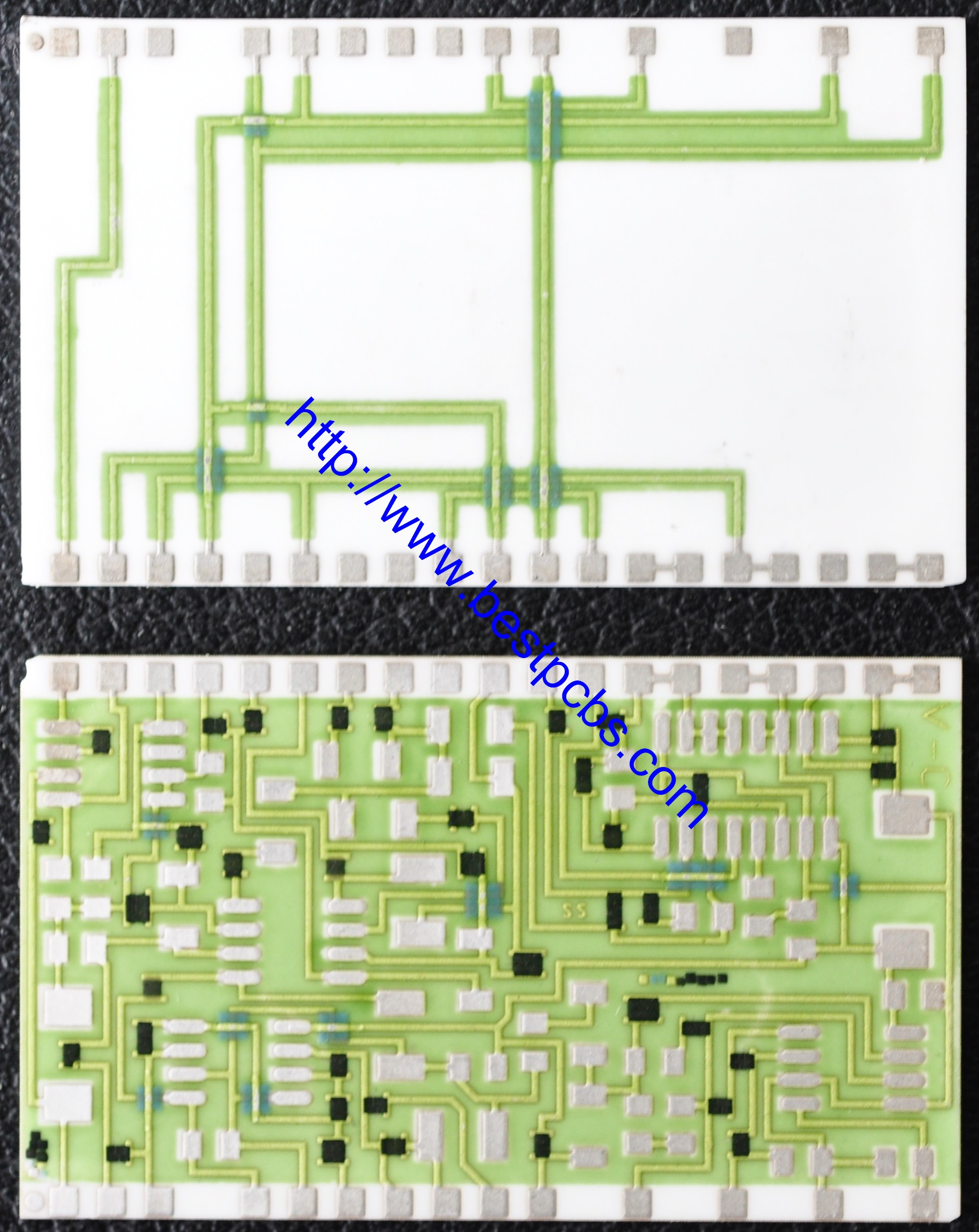
A thick film ceramic PCB is made by screen-printing functional pastes onto a ceramic base and then sintering the printed layers at high temperature. After firing, the material forms durable conductive paths or functional structures on the ceramic surface. In simple terms, a thick film ceramic circuit board combines the stability of a ceramic base with printed electrical features that can support conductors, resistors, and other functional layers.

The term “thick film” refers to the thickness of the printed conductive or resistive layer. In most cases, the conductor thickness starts at around 10 μm and often falls in the 10 to 13 μm range, with some designs reaching 20 μm. This is thicker than the metallization used in thin-film ceramic technology, but still thinner than the copper structure commonly found in DCB ceramic boards or standard FR4 boards.

A thick film ceramic substrate can do more than carry conductor traces. It can also support:

  • Conductors
  • Printed resistors
  • Dielectric layers
  • Cross-over conductors
  • Semiconductor-related functional structures

Because of this flexibility, thick film ceramic PCB is widely used in hybrid modules, sensor circuits, and compact control electronics.

What Is a Thick Film Ceramic PCB?

Thick Film vs Thin Film Ceramic PCB

The comparison between thick film vs thin film ceramic PCB is one of the most common questions in ceramic electronics. Although both technologies use ceramic materials as the base, their process routes, cost structures, and application focus are quite different.

ItemThick Film Ceramic PCBThin Film Ceramic PCB
Main ProcessScreen printing + firingVacuum deposition or sputtering
Typical Conductor Thickness10–20 μmMuch thinner
Cost PositionMore economical for many industrial usesUsually higher
Printed Resistor IntegrationEasyLess common
Fine-Line CapabilityModerateHigher
Typical UseHybrid circuits, sensors, power-related modulesPrecision circuits and ultra-fine patterns

In practical use, thick film ceramic PCB is often selected when the design needs better functional integration, a stable ceramic base, and a more workable cost. Thin film ceramic PCB is more suitable when very fine line resolution or higher pattern precision is the priority.

What Materials Are Used in an Alumina Ceramic Thick Film PCB?

An alumina ceramic thick film PCB is the most common version of this technology. The substrate is usually made from 96% or 98% alumina, because alumina offers a strong balance of electrical insulation, thermal resistance, and manufacturing practicality. For applications that require higher thermal conductivity, AlN is also a common choice. In some specialized cases, beryllium oxide may be used as well.

Common Substrate Materials

MaterialTypical FeatureNotes
96% AluminaStandard industrial choiceGood balance of cost, insulation, and manufacturability
98% AluminaHigher purityBetter stability for more demanding designs
AlNHigh thermal conductivityOften used in high-power modules and applications with strict heat dissipation needs
BeOExcellent thermal conductivityUsed in specialized applications with stricter handling and safety requirements

Common Substrate Thickness Options

  • 0.25 mm
  • 0.38 mm
  • 0.50 mm
  • 0.635 mm
  • 0.76 mm
  • 1.0 mm
  • 1.6 mm or 2.0 mm as custom options

Common Conductor Materials

Conductor MaterialTypical Use
Silver-PalladiumCommon and more cost-effective
Gold-PalladiumPremium applications and bonding-friendly designs
Mo/Mn + NiCertain special environments, including ozone-related use

The choice of thick film ceramic substrate material affects both cost and performance. For example, gold-palladium is far more expensive than silver-palladium, so it is generally used only when the application truly needs its bonding or performance advantages.

What Are the Main Technical Parameters in Thick Film PCB Manufacturing?

When evaluating thick film PCB manufacturing capability, engineers usually focus on conductor thickness, minimum line width, resistor integration, and possible layer count. These factors directly affect whether the board can match the intended circuit design.

ParameterTypical Capability
Substrate Material96% / 98% Alumina, AlN, BeO
Conductor Thickness≥10 μm, up to 20 μm
Standard Trace/Space0.30 / 0.30 mm
Finer Production Capability0.20 / 0.20 mm with higher cost
Prototype Fine Line0.15 / 0.20 mm in limited cases
Final Trace Layout Tolerance±10%
Typical Layers1L and 2L
Maximum LayersUp to 10L
PTHAvailable for selected multilayer or double-sided designs
Solder MaskOptional
Solder Mask ColorSemi-transparent
Solder Mask Heat ResistanceAbove 500°C

These parameters show why thick film PCB manufacturing is well suited to many industrial, automotive, lighting, and sensor-related designs. It is not aimed at ultra-fine microelectronic geometry, but it offers very good process stability for a broad range of practical applications.

Can a Thick Film Printed Resistor Ceramic Board Integrate Different Resistor Values?

Yes. One of the strongest advantages of a thick film printed resistor ceramic board is that resistor elements can be integrated directly onto the ceramic surface. This means one substrate can carry conductors and resistors together, reducing the need for extra discrete components in some designs.

A thick film printed resistor ceramic board can include:

  • A single resistor value across the entire design
  • Different resistor values in different circuit areas
  • Combined conductor and resistor functions on one substrate

That is why thick film ceramic PCB is often used in resistor cards, hybrid circuits, analog control modules, and sensor products. At the same time, resistor complexity affects cost. In general, the more resistor values placed on one board, the more difficult the process becomes, and the higher the price is likely to be.

Can a Thick Film Printed Resistor Ceramic Board Integrate Different Resistor Values?

Can Thick Film Ceramic PCB Support Wire Bonding?

Yes, thick film ceramic PCB can support wire bonding, but the requirement should be defined early. Both gold-palladium and selected silver-palladium conductor systems can support gold wire bonding, although not every standard conductor paste is equally suitable for that purpose.

If wire bonding is required, the supplier should know this during quotation and engineering review. That early confirmation helps with:

  • Correct conductor system selection
  • Better process compatibility
  • Improved bonding reliability in production

For bonding-related projects, early material matching is always more effective than changing the design later.

What Board Structures Are Available for a Thick Film Hybrid Circuit Board?

A thick film hybrid circuit board is most commonly produced as a 1-layer or 2-layer design, but multilayer structures are also possible for more complex projects. Because a ceramic thick film circuit can integrate conductors and resistor functions on the same substrate, it is often chosen for compact modules that need both electrical function and dimensional stability.

Common Build Styles

  • Single-sided thick film hybrid circuit board
  • Double-sided thick film ceramic PCB
  • Multilayer ceramic thick film circuit structures
  • PTH-supported designs for selected projects
  • Optional solder mask upon request

Shape and Delivery Notes

  • Rectangular boards are the most common format
  • Boards can be shipped as single pieces
  • Boards can also be delivered in panel form

For standard production, rectangular shapes are usually the easiest to process, inspect, and ship. In most cases, they also provide the best balance between manufacturing efficiency and handling convenience.

What Are the Most Common Thick Film Ceramic PCB Applications?

Thick film ceramic PCB applications are broad, especially in products that need heat resistance, electrical stability, and compact function integration. Because the ceramic base can remain stable under demanding conditions, this technology is widely used across industrial and automotive sectors.

Typical Applications

  • High-power LED
  • Street light
  • High-brightness lighting
  • Automotive light systems
  • Hybrid integrated circuits for automotive
  • Fuel sender resistor card
  • Injection systems
  • Anti-lock braking systems
  • High-power semiconductor modules
  • Electric power transmitter modules
  • Semiconductor process equipment
  • Solar cell applications
  • Sensors
  • Telecommunication devices
  • Chip and wafer-related electronic applications

What Affects the Cost of Thick Film Ceramic PCB?

The cost of thick film ceramic PCB depends on material selection, conductor system, resistor design, and processing difficulty. Even when two projects look similar on the surface, their price can change noticeably if the conductor material, resistor count, or line definition is different.

Main Cost Factors

  • Gold-palladium is much more expensive than silver-palladium
  • More resistor values on the same board increase cost
  • Finer trace and spacing increase process difficulty
  • More layers add complexity
  • Special substrate thickness adds cost
  • Bonding-compatible conductor systems may require special materials
  • Small prototype runs with fine features often cost more per piece

For many engineers, thick film ceramic PCB offers a useful performance upgrade over standard boards without reaching the cost level of DCB in many practical use cases.

What Should Buyers Confirm Before Ordering?

A clear design review before production helps avoid rework, shorten communication time, and improve quotation accuracy. This is especially important for ceramic projects, where material and conductor choices directly affect the process route.

Buyer Checklist

  • Substrate material
  • Ceramic purity
  • Substrate thickness
  • Conductor material
  • Conductor thickness requirement
  • Minimum trace and spacing
  • Number of resistor values
  • Whether wire bonding is required
  • Whether PTH is needed
  • Layer count
  • Solder mask requirement
  • Single-piece or panel delivery

If you are interested in thick film ceramic PCB, please contact us today for more information about Thick Film Ceramic circuit board.

You may also like

2 Layer SinkPAD Board

March 24th, 2026

A 2 Layer SinkPAD board is a copper-based PCB structure designed for applications that need both strong thermal performance and more routing space on a compact layout. It features two circuit layers built on the same side of the board, combined with a dielectric insulation layer and a copper core or raised copper pedestal.

Unlike conventional metal core PCBs, the thermal pad of the LED in a 2 Layer SinkPAD board is placed directly on the copper core. This creates a direct thermal path, allowing heat to move away from the LED much faster. Because of this structure, the board is widely used in thermoelectric separation designs where electrical routing and thermal transfer need to be handled independently.

What Is a 2 Layer SinkPAD Board?

A 2 Layer SinkPAD board is a single-sided direct thermal path PCB with two copper trace layers arranged on the same side. Although it contains two routing layers, it is still considered a single-sided SinkPAD PCB because both circuit layers are located on the top side of the board.

The main advantage of this construction is that it combines electrical isolation with direct heat conduction. The circuit traces remain electrically insulated through the dielectric layer, while the LED thermal pad contacts the copper base directly.
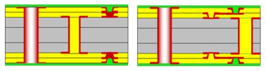
Compared with a 1 Layer SinkPAD board, the 2-layer version supports more complex circuit routing on the same board size. That makes it a practical choice for compact, high-power lighting designs where both thermal control and circuit density matter.

2 Layer SinkPAD Board

2 Layer SinkPAD Board

How Does a 2 Layer SinkPAD Board Work?

The board works by separating the electrical path from the thermal path. Electrical signals move through the copper trace layers, while heat generated by the LED or power device is transferred directly into the copper core.

Since copper has very high thermal conductivity, around 400 W/m.K, heat can spread quickly from the hot spot to the base metal. From there, it can be transferred to a heatsink, mounting surface, or surrounding air. The direct contact design improves thermal efficiency far beyond what is possible with standard MCPCB structures. As a result, the LED junction temperature can be controlled more effectively.

Why Choose a 2 Layer SinkPAD Board Instead of a Standard MCPCB?

A standard metal core PCB usually includes a dielectric layer between the heat source and the metal base. That structure provides insulation, but it also adds thermal resistance. In a 2 Layer SinkPAD board, the thermal pad touches the copper pedestal directly, so heat does not need to pass through the dielectric in the same way.

This creates several practical benefits:

  • Lower thermal resistance
  • Better heat dissipation for high-power LEDs
  • More stable light output
  • Longer service life of the lamp
  • Higher routing density on the same board area
  • Better support for compact and advanced circuit design

For engineers working on high-power lighting modules, automotive lighting, or dense LED arrays, this structure offers a more efficient thermal solution without sacrificing design flexibility.

https://www.youtube.com/watch?v=KFQNdAvZGEA

Advantages of Using 2 layers SinkPAD Board

  • The metal core is Copper with high density, strong thermal carrying capacity and higher thermal conductivity. So the volume can be smaller under the same power.
  • It adopts the thermoelectric separation structure, the Lumens depreciation of the LED is minimized, and the life of the lamp is prolonged.
  • Suitable for matching single high-power lamp, such as Cree XPL, XML, XHP; Osram LED, etc., also COB package LED
  • High power semiconductors (transistors, thyristors, diodes) as well as resistors.
  • A variety of Surface Finishing are available according to different demands. (ENIG, OSP, Immersion Tin, ENEPIG, HAL) with excellent reliability of the surface treatment layer.
  • Different structures can be made according to different design needs of LED. (Such as copper bump, copper concave block)
  • Put more circuits on the same side, design more complicated circuit board.

Typical Applications of 2 Layer SinkPAD Board

A 2 Layer SinkPAD board is commonly used in products that require both strong thermal conductivity and compact circuit design.

Typical applications include:

  • High power LED modules up to 200W
  • COB LED lighting
  • Single high-power LEDs such as Cree XPL, XML, XHP, and Osram LEDs
  • Automotive lighting systems
  • Industrial lighting equipment
  • Power semiconductor modules
  • High-power resistor circuits
  • Thermoelectric separation applications

Because of its copper direct thermal path structure, this board is especially useful in lighting products where heat buildup directly affects brightness consistency and service life.

2 Layer SinkPAD Board Stack-Up

The typical stack-up of a 2 Layer SinkPAD board includes:

  • Two copper circuit trace layers on the same side
  • Dielectric insulation layer
  • Copper core or copper pedestal
  • Direct thermal contact area under the LED thermal pad
2 Layer SinkPAD Board Stack-Up

This stack-up is designed to achieve both electrical isolation and rapid heat transfer. It is one of the main reasons this board performs much better than ordinary aluminum PCB or traditional MCPCB in high thermal load applications.

Our 2 Layer SinkPAD Board Capability

ItemCapability
Base MaterialCopper
Copper Base Thickness0.8mm, 1.0mm, 1.2mm, 1.4mm, 1.5mm
Thermal Conductivity400 W/m.K
Board Thickness1.0mm to 2.0mm
Copper Thickness0.5 oz, 1 oz, 2 oz, special 3 to 10 oz
Outline ProcessingRouting, Punching, V-Cut
Solder Mask ColorWhite, Black, Blue, Green, Red
Silkscreen ColorBlack, White, Yellow
Surface FinishImmersion Gold, ENEPIG, Immersion Tin, OSP
Max Panel Size600 x 500mm
PackingVacuum packing, plastic bag
Sample Lead Time1.5 to 2 weeks
Mass Production Lead Time2 to 3 weeks

Why Is 2 Layer SinkPAD Board a Good Choice for High-Power LED Design?

In high-power LED products, heat is often the main factor that limits performance. Excessive temperature can reduce brightness, accelerate lumen depreciation, and shorten product lifespan. A 2 Layer SinkPAD board helps solve this issue by allowing heat to move directly into the copper base without unnecessary thermal barriers.

At the same time, the two-layer trace design gives more room for routing, which is useful when the LED module includes more complex circuitry. It is especially suitable for high-power LED modules, COB lighting, and power semiconductor applications where thermal performance directly affects reliability and lifespan. For projects that need both strong heat dissipation and more circuit freedom, a 2 Layer SinkPAD board is a highly effective choice.

FAQs about 2 Layer SinkPad MCPCB

1. What is a 2 Layer SinkPAD Board?

A 2 Layer SinkPAD Board is a high-power Metal Core PCB (MCPCB) that features two copper circuit layers on one side of a metal base. Unlike standard 2-layer MCPCBs where a dielectric layer separates all components from the metal core, the SinkPAD design “sinks” the thermal pad of a component through the dielectric, creating a Direct Thermal Path (DTP) to the copper or aluminum base.

2. How does a 2 Layer SinkPAD differ from a Single Layer SinkPAD?

While a single-layer SinkPAD only allows for simple circuit routing, a 2 Layer SinkPAD provides an additional copper layer for complex circuit design. This allows for more sophisticated power management, signal routing, or the placement of control components on the same board as high-power LEDs or transistors, all while maintaining the ultra-low thermal resistance of a direct-to-metal connection.
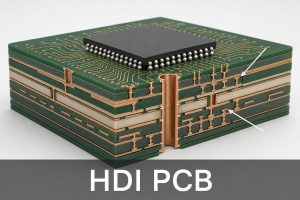
3. What are the thermal conductivity benefits of a 2 Layer SinkPAD?

Because the thermal pad of the component bypasses the 1–8 W/m·K dielectric layer and sits directly on the metal core, the effective thermal conductivity can reach 400 W/m·K (using a copper base). This is significantly higher than a standard 2-layer MCPCB, which is limited by the thermal resistance of the thin prepreg or dielectric layer required for circuit isolation.
4. Can I use Plated Through Vias (PTH) on a 2 Layer SinkPAD Board?

Yes, 2 Layer SinkPAD boards support inter-layer vias to connect the two copper circuit layers. However, these vias are typically used for electrical signals or low-power traces. The primary heat dissipation is still handled by the pedestal (the “SinkPAD”) that connects the high-power component’s thermal pad directly to the metal substrate, rather than relying on thermal vias.

5. When should I choose a 2 Layer SinkPAD over a standard FR4 with thermal vias?

You should choose a 2 Layer SinkPAD when your components generate heat that exceeds the capacity of FR4 (typically >3W per LED). While FR4 with thermal vias is cheaper, it cannot match the thermoelectric separation efficiency of a SinkPAD. If your application involves high-density power electronics where space is limited and active cooling is not an option, the 2-layer SinkPAD is the superior choice for reliability.

6. How does a 2 Layer SinkPAD differ from a Double-Sided SinkPAD PCB?

The primary difference lies in the circuit density versus mounting capability.

  • 2 Layer SinkPAD: Features two copper circuit layers (Top & Bottom) on one side of the metal base. It is designed for complex circuitry that requires more routing space or inter-layer connections (vias) while still maintaining a Direct Thermal Path (DTP) for high-power components on the top side.
  • Double-Sided SinkPAD: Features circuit layers and component mounting pads on both sides of the metal core (Top and Bottom). This allows you to mount high-power components, like LEDs or transistors, on both surfaces of the board, with each side utilizing the central metal core for heat dissipation.

You may also like

Double Sided SinkPAD Board

March 24th, 2026

What Double Sided SinkPAD Board is?

The Double sided SinkPAD board consists of at least two layers of trace circuit, and there’re at least one circuit layer on both top and bottom side of board, a dielectric (non-conducting) layer, a metal core/pedestal which normally is copper.

As there’re circuit layer on both sides, so engineer can put more (about 2 times, ideally) components on the same size circuit to realize more function, more complicated design, comparing to 1 Layer SinkPAD board or 2 layers SinkPAD board.

Double Sided SinkPAD Board

There’s no PTH (plated through hole) on double sided SinkPAD board, because the limitation of manufacturing process, which different from double sided Metal Core PCB which has a lot of PTH, and thermal PAD of LED will be put directly on copper core, also belonging to Direct Thermal Path (DTP) board too, but engineer needs to consider where the heat sink will be if he want more fast heat transferring, as there’re always components on both sides, and that make double sides SinkPAD board designing becoming more difficult & complex comparing to 1L SinkPAD board, or 2L SinkPAD board.

Stack up of Double Sided SinkPAD Board

Double Sided SinkPAD Board

Advantages of Utilizing Double Sided SinkPAD Board:

  • Put more components on the both top and bottom, design more complicated circuit board.
  • It adopts the thermoelectric separation structure, the Lumens depreciation of the LED is minimized, and the life of the lamp is prolonged.
  • Suitable for matching single high-power lamp, such as Cree XPL, XML, XHP; Osram LED, etc., also COB package LED
  • High power semiconductors (transistors, thyristors, diodes) as well as resistors.
  • A variety of Surface Finishing are available according to different demands. (ENIG, OSP, Immersion Tin, ENEPIG, HAL) with excellent reliability of the surface treatment layer.

Application of Double Sided SinkPAD Board

  • High Power LED (up to 200W).
  • High semiconductors (transistors, thyristors, diodes) as well as resistors.

2 Layer SinkaPAD Board Capability

  • Base material: Copper: 0.8mm, 1.0mm, 1.2mm, 1.4mm, 1.5mm
  • Thermal Conductivity: 400 W/m.K.
  • Board Thickness: 1.0mm~2.0 mm (0.04″~0.08″)
  • Copper thickness: 0.5 OZ, 1.0 OZ, 2.0 OZ (specially 3-10 OZ)
  • Outline: Routing, punching, V-Cut
  • Soldermask: White/Black/Blue/Green/Red Oil
  • Legend/Silkscreen Color: Black/White/Yellow
  • Surface finishing: Immersion Gold, ENEPIG, Immersion Tin, OSP
  • Max Panel size: 600*500mm(23.62″*19.68″)
  • Packing: Vacuum/Plastic bag
  • Samples L/T: 1.5~2 weeks
  • MP L/T: 2-3 weeks

Click here to see the manufacturing process of double sided SinkPAD Board and other options.

If you want to customize double sided SinkPAD board, please contact EBest Circuit (Best Technology) today send your request for double sides SinkPAD PCB.

FAQs about Double-Sided SinkPAD Boards

1. What is a Double-Sided SinkPAD Board and how does it work?

A Double-Sided SinkPAD Board is a specialized Metal Core PCB (MCPCB) that provides a Direct Thermal Path (DTP) on both sides of the board. Unlike standard MCPCBs that use a dielectric layer to separate the circuit from the metal base, SinkPAD technology removes the dielectric under the component’s thermal pad. This allows the component (like a high-power LED) to sit directly on the copper or aluminum core, drastically reducing thermal resistance.

2. How does a Double-Sided SinkPAD differ from a standard Double-Sided MCPCB?

The primary difference is the thermal conductivity. In a standard double-sided MCPCB, heat must travel through a thermally conductive dielectric layer (typically 1–8 W/m·K) to reach the metal core. In a SinkPAD board, the dielectric is bypassed entirely for the thermal pad, allowing for conductivity ratings as high as 400 W/m·K (if using a copper core). Additionally, double-sided SinkPADs allow for higher component density by utilizing both the top and bottom layers for active circuitry.

3. Why would I choose a double-sided design over a single-layer SinkPAD?

Engineers choose double-sided SinkPADs when they need to maximize functional density in compact spaces. It allows for roughly twice the component population or more complex circuit routing compared to a 1-layer board. This is ideal for high-power applications where you need to mount LEDs or transistors on one side while placing control circuitry, connectors, or additional power components on the other.

4. Are there limitations to the Plated Through Holes (PTH) in double-sided SinkPADs?

Yes. Due to the unique manufacturing process where the metal core is “sunk” or embossed to meet the trace layer, standard Plated Through Holes (PTH) are often limited or more complex to implement than in traditional FR4 boards. Connections between sides are typically handled through specialized routing or assembly techniques, so it is crucial to consult with your manufacturer during the design phase to ensure the layout is compatible with the “thermoelectric separation” structure.

5. Which base material is better for SinkPAD boards: Aluminum or Copper?

  • Copper: Best for ultra-high-power applications. It offers superior thermal conductivity (approx. 400 W/m·K) and is the most common choice for SinkPAD convexity because it is easier to etch and process for this specific technology.
  • Aluminum: More cost-effective and lighter. While it has good thermal properties, the chemical process for creating the SinkPAD convexity is more complex, often making it more expensive or difficult to produce than copper-based SinkPADs.

6. Can SinkPAD technology be used for components other than LEDs?

Absolutely. While most commonly used for high-power LEDs (Cree, Osram, etc.) to prevent lumen depreciation, SinkPAD boards are excellent for any high-power semiconductor that features an electrically neutral thermal pad. This includes power transistors, thyristors, diodes, and high-wattage resistors used in automotive, aerospace, or industrial power monitoring.

You may also like

Multi Layer Metal Core PCB

March 24th, 2026

Just like FR4 PCB, we can also make boards with more than 2 layers of traces and we named it “Multi Layers MCPCB“. The structure is similar with FR4 Multi Layers, but it much more complex to make.

You can populated more components on the boards, put signal and ground layer into seperated layers, to achieve better performance in electrical performance.

Compared with normal FR4, this sturcture need more technology and experience on laminating of more than two layers together with metal core and the cost is much higher than 2 layers MCPCB or double sided MCPCB.

Structure of Multi Layers MCPCB

Multi Layer Metal Core PCB

Capability of Multi Layers MCPCB

  • Base material: Aluminum/Copper/Iron Alloy
  • Thermal Conductivity (dielectrial layer): 0.8, 1.5, 2.0, 3.0 W/m.K.
  • Board Thickness: 0.8mm~3.0mm(0.02″~0.12″)
  • Copper thickness: 0.5 OZ, 1.0 OZ, 2.0 OZ, 3.0 OZ
  • Outline: Routing, punching, V-Cut
  • Soldermask: White/Black/Blue/Green/Red Oil
  • Legend/Silkscreen Color: Black/White
  • Surface finishing: Immersion Gold, HASL, OSP
  • Max Panel size: 600*500mm(23.62″*19.68″)
  • Packing: Vacuum/Plastic bag
  • Samples L/T: 15~18 Days
  • MP L/T: 15~20 Days

FAQs

1. What is a multi-layer MCPCB and how does it differ from standard FR4?

A multi-layer MCPCB consists of multiple copper conductive layers separated by high-thermal-conductivity dielectric layers, all bonded to a metal base (usually Aluminum or Copper). Unlike standard FR4, which relies on the epoxy glass substrate for structure, an MCPCB uses the metal base as a heat sink. While FR4 is an insulator with poor thermal management, the metal core in an MCPCB allows for heat dissipation rates that are significantly higher, making it essential for high-power electronics.

2. What are the typical thermal conductivity levels for multi-layer MCPCBs?

The thermal performance of a multi-layer MCPCB is primarily determined by the dielectric layer rather than the metal base itself. Standard dielectric materials offer conductivity between 1.0 W/mK and 3.0 W/mK. However, high-performance multi-layer stacks used in automotive or aerospace applications can reach 4.0 W/mK to 8.0 W/mK. Choosing the right dielectric is a balance between thermal efficiency and the breakdown voltage required for the circuit.

3. How many layers can be integrated into a Metal Core PCB?

Technically, “multi-layer” in the context of MCPCBs typically refers to 2-layer or 4-layer configurations. While it is possible to go higher, the complexity increases significantly because all heat must eventually pass through the dielectric layers to reach the metal base. In a 4-layer stack, the inner layers are further from the heat sink, which can lead to thermal bottlenecks if the design does not utilize thermal vias effectively.

4. Can you use plated through-holes (PTH) in a multi-layer MCPCB?

Yes, but the process is more complex than with standard PCBs. To prevent short-circuiting the signals to the metal core, the metal base must be pre-drilled and filled with an epoxy resin before the copper layers are laminated. Then, a smaller hole is drilled through the resin plug and plated. This creates an “insulated via” that allows signals to pass through the metal core safely.

5. What are the main applications for multi-layer MCPCB designs?

Multi-layer MCPCBs are the go-to solution when space is limited but power density is high. Common applications include:

  • Automotive: LED headlight systems and power converters (EV/HEV).
  • Power Supplies: High-voltage regulators and heavy-duty industrial rectifiers.
  • Aerospace: Power distribution units where weight and heat must be managed simultaneously.
  • Medical: High-intensity surgical lighting and imaging equipment.

6. What are the manufacturing challenges of multi-layer MCPCBs?

The primary challenge is coefficient of thermal expansion (CTE) mismatch. Metal bases (Aluminum/Copper) expand at different rates than the copper traces and dielectric during the lamination process. This can lead to delamination or bowing of the board. Precise control over the pressing cycle and the use of specialized “no-flow” or “low-flow” prepregs are required to ensure the structural integrity of the multi-layer stack.

You may also like

Double Sided Metal Core PCB

March 20th, 2026

A double sided metal core PCB also has same two layers of copper conductor like Double layers MCPCB, but the metal core is in the middle of two conductor, so there’re conductors (trace) on both sides of metal core, and were connected to each other by Vias. So we named it “Double sided MCPCB”, and you can populated SMD on both top and bottom.

Different with Single layer MCPCB, double sided MCPCB also requires an additional pressing step to laminate the imaged thermal conductive laminate and metal core (also known as metal base) together. But sometimes, some raw Metal Clad material vendor will supply board material which already laminated.

Compared with normal FR4, this structure need more technology and experience on laminating of two layers together with metal core.

Structure of Double Sided MCPCB

Structure of Double Sided MCPCB

Capability of Double Sided MCPCB

  • Base material: Aluminum/Copper/Iron Alloy
  • Thermal Conductivity (dielectric layer): 0.8, 1.5, 2.0, 3.0 W/m.K.
  • Board Thickness: 0.5mm~3.0mm (0.02″~0.12″)
  • Copper thickness: 0.5 OZ, 1.0 OZ, 2.0 OZ, 3.0 OZ, 4.0 OZ, 5.0 OZ
  • Outline: Routing, punching, V-Cut
  • Solder mask: White/Black/Blue/Green/Red Oil
  • Legend/Silkscreen Color: Black/White
  • Surface finishing: Immersion Gold, HASL, OSP
  • Max Panel size: 600*500mm (23.62″*19.68″)
  • Packing: Vacuum/Plastic bag
  • Samples L/T: 10~15 Days
  • MP L/T: 12~15 Days

FAQs about Double sided Metal Core PCB

1. What is a double-sided metal core PCB?

A double-sided MCPCB consists of two circuit layers (top and bottom) with a metal core—typically aluminum or copper—sandwiched in the middle. Unlike standard FR4 boards, the metal core acts as a high-efficiency heat sink. The layers are connected using insulated through-holes or thermal vias to ensure electrical signals pass through without shorting against the metal base.

2. How does a double-sided MCPCB differ from a single-sided one?

The primary difference lies in component density and routing complexity.

  • Single-Sided: Components are on one side; the metal base is on the back. It is simpler and cheaper but limited in space.
  • Double-Sided: Allows for components and traces on both sides of the metal core. This is necessary for complex designs where high power density requires cooling for components on both surfaces of the board.

3. What materials are used for the core in double-sided PCBs?

The three most common materials are:

  • Aluminum (6061 or 5052): The most cost-effective and popular choice, offering good thermal conductivity and mechanical stability.
  • Copper: Offers superior thermal conductivity (nearly double that of aluminum) but is significantly heavier and more expensive.
  • Stainless Steel: Used primarily for its mechanical strength and corrosion resistance, though its thermal performance is lower than aluminum.

4. Why are double-sided MCPCBs used instead of standard FR4?

Standard FR4 is a poor thermal conductor. In high-power applications, heat builds up and can cause component failure. Double-sided MCPCBs are used because the metal core can dissipate heat at rates of 1.0 W/mK to 9.0 W/mK (or higher), whereas FR4 typically manages only 0.25 W/mK. This allows for smaller form factors without overheating.

5. What are the main applications for double-sided metal core PCBs?

These boards are a staple in industries where heat management is critical:

  • Automotive: LED headlights, power converters, and motor control modules.
  • Lighting: High-output street lights and industrial floodlights.
  • Power Electronics: Solid-state relays, rectifiers, and high-capacity power supplies.
  • Telecommunications: Signal amplifiers and high-frequency filtering equipment.

6. What are the manufacturing challenges of double-sided MCPCBs?

The most significant challenge is the drilling and insulation process. Because the core is conductive metal, every through-hole must be pre-drilled, filled with a specialized dielectric resin, and then re-drilled to prevent the copper pins from touching the metal core. This requires high precision and specialized lamination techniques to ensure the board does not delaminate under thermal stress.

You may also like

COB MCPCB

March 20th, 2026

What is Chip On Board COB MCPCB?

COB MCPCB, known as “Chip-On-Board” Metal Core PCB, is a type of MCPCB used in thermoelectric separation application. By using COB MCPCB, the micro-chip (also known as “die”) directly touch the metal core where the heat dissipate, and electrically interconnect the trace of circuit board (wire-bonding) so that power supply can be provided.
In normal MCPCB, there’s a dielectric layer between trace copper and metal core, and the thermal conductivity is limited by that dielectric layers, so value can only be 1~3 W/m.K. But using COB MCPCB, there’s no such dielectric layer because chip (die) direct touch the metal core, so thermal conductivity value of COB MCPCB will be almost the same one of metal core material itself. The normal material of metal core is aluminum, so thermal conduviity of COB MCPCB is more than 200W/m.K.

COB MCPCB

COB MCPCB (Chip on Board)

What are the COB Wire Bonding Processes?

COB process consists of three main categories to perform when manufacturing the Chip-on-Board:

1st: die mount or die attach;

2nd: wire bonding;

3rd: the encapsulation of die wires.

By using wire bonding & epoxy packaging then directly embedded on MCPCB, this practice can extend the lifespan of LED and unified light emission.

According to process and material, COB MCPCB applications can be categorized into two types: Mirror Aluminum and silver or gold platting aluminum, or silver plating mirror aluminum PCB.
Structure of COB MCPCB

Structure of COB MCPCB

Advantage of utilizing COB MCPCB

  • Excellent heat dissipation
  • High thermal conductivity: 137W/m.K
  • Higher reliability with better heat dispatch and small number of solder joint.
  • Provide enhanced reliability and lifespan of LED
  • Easy assembly for high powers LEDs
  • High quality material and production process allows easy assembly and substantial reduce the error percentage in assembly process
  • Substantially reduced space and cost
  • With better security protection (difficult to hack using reverse engineering)
  • Shorter time to the market

Application of COB MCPCB

  • High Power LED (up to 200W)
  • LED Backlight for LED TV
  • LED Front Light for E-Book
  • Agriculture & Horticulture Lighting
  • Street & Parking Lot Lighting
  • Automotive
  • Power Supply
  • ustomer Electronics Lighting
  • Other products that require thermal solutions
Application of COB MCPCB

FAQs about COB MCPCBs

1. What is the difference between a standard MCPCB and a COB MCPCB?

A standard MCPCB (Metal Core PCB) usually has SMT (Surface Mount Technology) components soldered onto a dielectric layer. In contrast, a COB (Chip-on-Board) MCPCB allows the LED semiconductor chip to be mounted directly onto the metal core or into a recessed “well.” This removes the thermal resistance of the LED package itself, allowing for much higher power density.

2. Why is thermal conductivity so important for COB MCPCBs?

Since COB LEDs pack many light-emitting diodes into a very small area, they generate intense localized heat. If this heat isn’t dissipated, the LED’s lifespan and brightness (luminous flux) drop rapidly. COB MCPCBs use materials like Aluminum or Copper to pull heat away from the chips at rates significantly higher than standard FR4 boards.

3. What are the common base materials used in COB MCPCBs?

  • Aluminum: The most common and cost-effective choice for general lighting.
  • Copper: Offers superior thermal conductivity but is heavier and more expensive; used for extreme high-power applications.
  • Stainless Steel: Occasionally used for high-strength requirements, though it has poorer thermal properties than Aluminum.

4. What is a “Mirror Aluminum” COB MCPCB?

A Mirror Aluminum COB MCPCB features a highly reflective, polished surface. This design ensures that light emitted from the sides of the LED chips is reflected forward, increasing the overall light output efficiency (Lumen/Watt) by reducing light absorption by the board itself.

5. Can COB MCPCBs be used with high-voltage applications?

Yes, but they require a specialized dielectric layer. This layer must be thin enough to allow heat to pass through to the metal core, but thick enough to provide electrical insulation (dielectric breakdown voltage) to prevent short circuits, especially in AC-driven LED modules.

6. What are the main applications for COB MCPCB technology?

Because they offer high brightness in a compact footprint, they are the industry standard for:

  • Automotive lighting (Headlights).
  • Industrial high-bay lighting.
  • Street lights and architectural floodlights.
  • Commercial downlights and track lighting.

You may also like

Single Layer MCPCB

March 20th, 2026

A simple layer single sided MCPCB consists of a metal base (usually aluminum, or copper alloy), Dielectric (non-conducting) Layer, Copper Circuit Layer, IC components and solder mask.

The prepreg dielectric provides excellent heat transfer from the foil and components to the base plate, while maintaining excellent electrical isolation. The base aluminum/copper plate gives the single-sided substrate mechanical integrity, and distributes and transfers the heat to a heat sink, mounting surface or directly to the ambient air.

The Single-Layer MCPCB can be used with surface mount and chip & wire components, and provides much lower thermal resistance than FR4 PWB. The metal core provides lower cost than ceramic substrates, and allows much larger areas than ceramic substrates.

Single Layer MCPCB

Single Layer MCPCB Capability

  • Base material: Aluminum/Copper/Iron Alloy
  • Thermal Conductivity (dielectrial layer): 0.8, 1.0, 1.5, 2.0, 3.0 W/m.K.
  • Board Thickness: 0.5mm~3.0mm(0.02″~0.12″)
  • Copper thickness: 0.5 OZ, 1.0 OZ, 2.0 OZ, 3.0 OZ, up to 10 OZ
  • Outline: Routing, punching, V-Cut
  • Soldermask: White/Black/Blue/Green/Red Oil
  • Legend/Silkscreen Color: Black/White
  • Surface finishing: Immersion Gold, HASL, OSP
  • Max Panel size: 600*500mm(23.62″*19.68″)
  • Packing: Vacuum/Plastic bag
  • Samples L/T: 4~6 Days
  • MP L/T: 5~7 Days

Single Layer MCPCB FAQs

1. What is a single layer MCPCB?

A single layer MCPCB consists of a metal base (typically aluminum or copper), a non-conductive dielectric layer, and a copper circuit layer. Unlike standard PCBs, the metal core acts as a primary heat sink, moving thermal energy away from high-power components to the environment or an external cooling system.

2. How does a single layer MCPCB differ from a standard FR4 PCB?

The primary difference is the substrate material. While FR4 uses fiberglass and epoxy, an MCPCB uses a metal base. This allows MCPCBs to have significantly higher thermal conductivity. While a standard FR4 board typically has a conductivity of around 0.25 W/mK, a single layer MCPCB can range from 1.0 W/mK to 9.0 W/mK depending on the dielectric material used.

3. What are the typical applications for single layer MCPCBs?

Single layer MCPCBs are most commonly used in the LED lighting industry (street lights, automotive headlamps, and backlight units) because LEDs generate significant heat that can degrade performance if not dissipated. They are also widely used in power conversion, solid-state relays, and the automotive sector for motor control modules.

4. Can you have plated through-holes (PTH) on a single layer MCPCB?

Generally, no. In a standard single layer MCPCB, the metal base is conductive, so through-holes would cause a short circuit between the signal layer and the base. Components are typically Surface Mount Devices (SMD). If through-hole components are required, specialized “COB” (Chip on Board) or complex insulated hole processes are needed, which significantly increases cost.

5. What are the layers of a single layer MCPCB?

A standard stack-up includes four main layers:

  • Solder Mask: Protects the copper circuit.
  • Circuit Layer: The copper foil used for traces.
  • Dielectric Layer: The most critical part; it provides electrical insulation while facilitating heat transfer.
  • Metal Substrate: Usually 1.0mm to 3.2mm of Aluminum (5052 or 6061) or Copper.

6. Is aluminum or copper better for the metal core?

Aluminum is the most popular choice because it is cost-effective and provides excellent thermal dissipation for most applications. Copper offers even higher thermal conductivity but is much heavier and more expensive. Copper is usually reserved for extremely high-power density applications where aluminum’s performance is insufficient.

You may also like