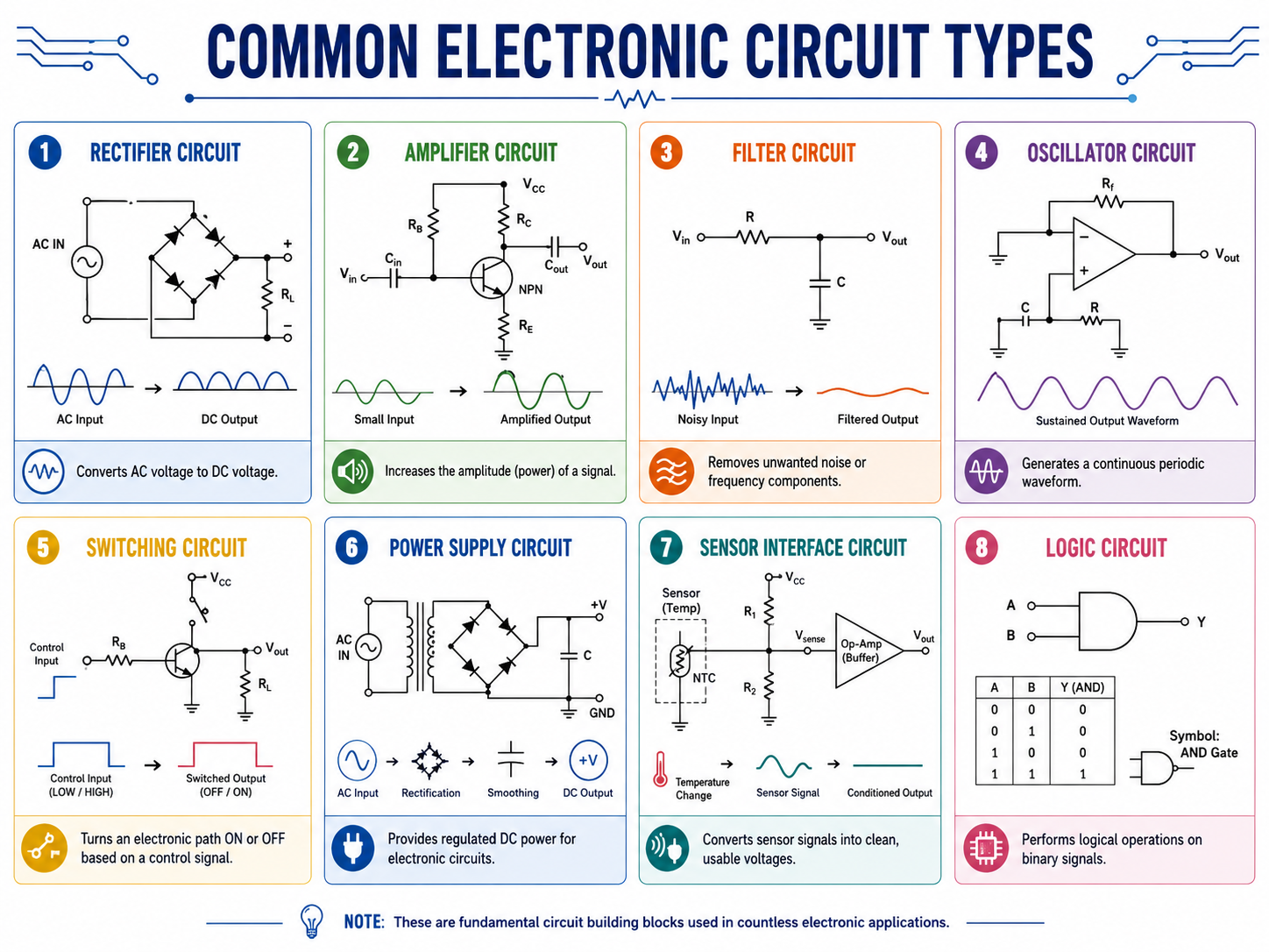
A 1k resistor color code is one of the first resistor markings many electronics beginners learn. It appears in LED circuits, Arduino projects, PCB prototypes, sensor modules, pull-up networks, pull-down networks, and many low-power electronic designs.
The value 1k means 1,000 ohms, also written as 1 kΩ. For a common 4-band resistor, the color code is:
Brown – Black – Red – Gold
For a 5-band precision resistor, the common color code is:
Brown – Black – Black – Brown – Brown
Both markings can represent a 1k ohm resistor, but the band count and tolerance are different. This guide explains how to read them clearly, how to identify a 1k resistor, how to test it, and how to understand its current and power limits.
What Is a 1k Resistor?
A 1k resistor is a passive electronic component with a resistance value of 1,000 ohms. Its job is to control current, divide voltage, set signal levels, protect components, and help circuits operate within safe electrical limits.
The letter k stands for kilo, which means one thousand. So when you see 1k resistor, it means:
1k resistor = 1,000 ohm resistor = 1 kΩ resistor
In real circuits, 1k resistors are extremely common because they offer a practical balance. They are large enough to limit current in many low-voltage circuits, yet small enough to allow useful signal flow.
You may find 1k resistors in:
- LED current-limiting circuits
- Microcontroller input and output circuits
- Pull-up and pull-down resistor networks
- Transistor base resistor designs
- Sensor interface circuits
- Audio and signal conditioning circuits
- PCB test circuits
- Prototype breadboard projects
In PCB assembly, 1k resistors are also widely used in surface-mount form. Instead of color bands, SMD resistors usually use printed numbers such as 102.
What Is a 1k Resistor Equal To?
A 1k resistor is equal to 1,000 ohms. It can also be written in several common ways depending on the circuit diagram, datasheet, BOM, or PCB silkscreen style.
| Marking | Meaning |
|---|---|
| 1k | 1,000 ohms |
| 1 kΩ | 1,000 ohms |
| 1000 Ω | 1,000 ohms |
| 1.0k | 1,000 ohms |
| 1K | 1,000 ohms |
| 102 on SMD resistor | 1,000 ohms |
| 0.001 MΩ | 1,000 ohms |
In schematics, engineers often write 1k because it is shorter and easy to read. In datasheets and formal electrical documents, you may see 1 kΩ.
For SMD resistors, the code 102 is very common. The first two digits are 10, and the third digit tells how many zeros to add. So:
102 = 10 + two zeros = 1000 ohms
That means an SMD resistor marked 102 is usually a 1k ohm resistor.
What Color Is a 1k Resistor?
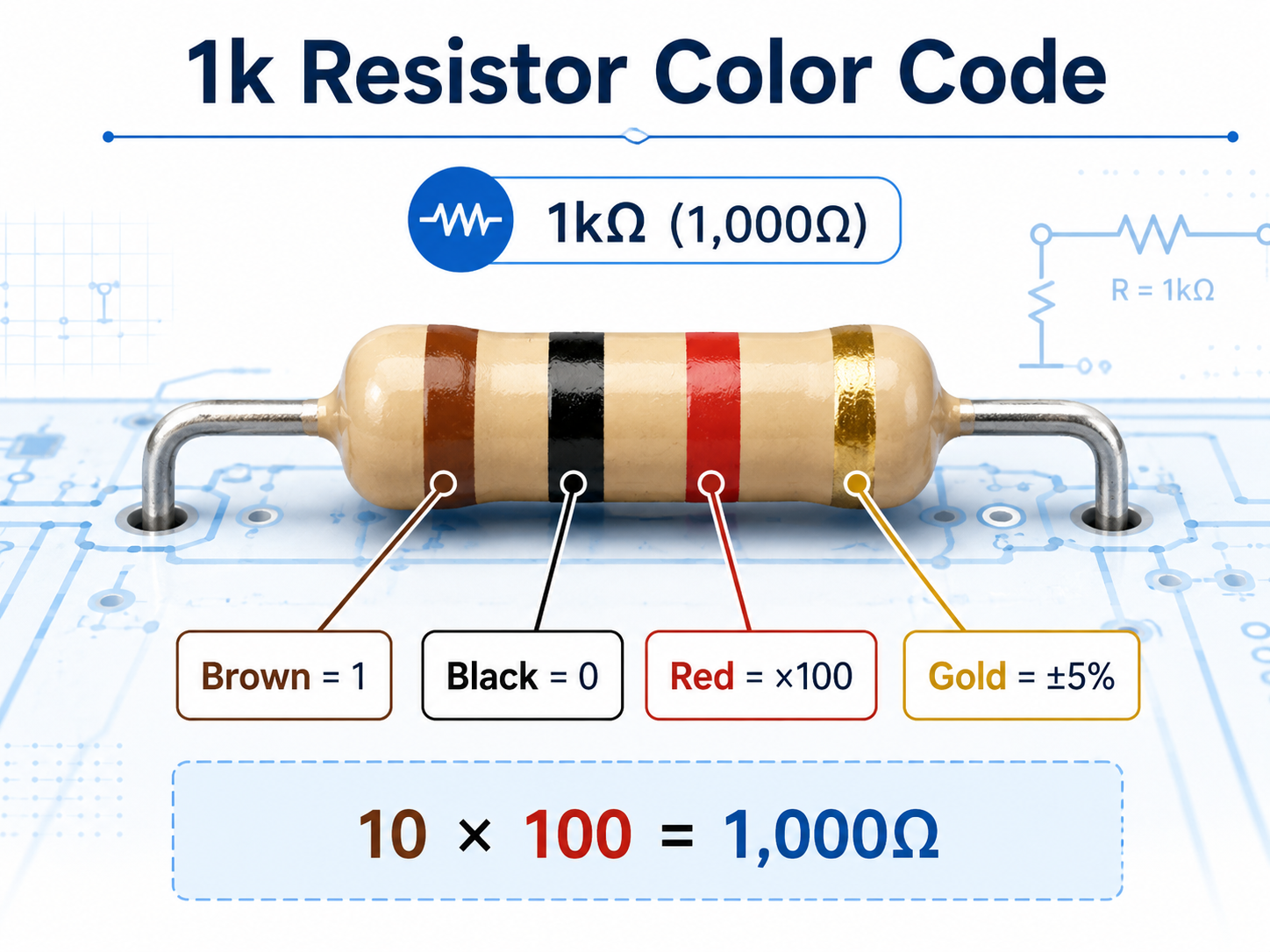
A standard 4-band 1k resistor usually has these colors:
Brown – Black – Red – Gold
Each color has a meaning:
| Band | Color | Meaning |
|---|---|---|
| 1st band | Brown | First digit: 1 |
| 2nd band | Black | Second digit: 0 |
| 3rd band | Red | Multiplier: ×100 |
| 4th band | Gold | Tolerance: ±5% |
So the value is:
10 × 100 = 1,000 ohms
The gold band means the resistor has a tolerance of ±5%. So a 1k resistor with gold tolerance can normally measure between:
950 ohms and 1,050 ohms
That is still considered acceptable for a ±5% resistor.
The body color of the resistor may vary. Many through-hole resistors have beige, tan, blue, green, or light-colored bodies. The body color itself is not the value. The colored bands provide the resistance information.
What Is the Color Code for a 1k Ohm Resistor?
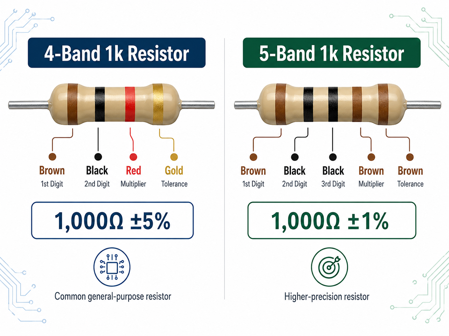
The standard resistor color code for 1k ohm depends on whether the resistor uses 4 bands or 5 bands.
For a common 4-band resistor, the color code is:
Brown – Black – Red – Gold
This is the most familiar version for general electronics work.
| Color | Number or Function |
|---|---|
| Brown | 1 |
| Black | 0 |
| Red | ×100 |
| Gold | ±5% tolerance |
Calculation:
1, 0, ×100 = 1,000 ohms
So the color code for 1k ohm resistor in 4-band format is:
Brown Black Red Gold
Some 1k resistors may use a different tolerance color. For example:
| 4-Band Color Code | Value | Tolerance |
|---|---|---|
| Brown Black Red Gold | 1kΩ | ±5% |
| Brown Black Red Brown | 1kΩ | ±1% |
| Brown Black Red Red | 1kΩ | ±2% |
| Brown Black Red Silver | 1kΩ | ±10% |
The first three bands still represent 1,000 ohms. The last band only changes the tolerance.
1k Resistor Color Code 5 Band
A 1k resistor color code 5 band version is usually used for precision resistors. A typical 5-band 1k resistor is:
Brown – Black – Black – Brown – Brown
Here is how it works:
| Band | Color | Meaning |
|---|---|---|
| 1st band | Brown | First digit: 1 |
| 2nd band | Black | Second digit: 0 |
| 3rd band | Black | Third digit: 0 |
| 4th band | Brown | Multiplier: ×10 |
| 5th band | Brown | Tolerance: ±1% |
Calculation:
100 × 10 = 1,000 ohms
So the value is again 1kΩ.
A 5-band resistor often provides better accuracy than a common 4-band resistor. For example, a 5-band 1k resistor with brown tolerance has a tolerance of ±1%. That means the acceptable measured range is usually:
990 ohms to 1,010 ohms
This tighter range is useful in circuits that need better precision, such as:
- Measurement circuits
- Voltage dividers
- Sensor conditioning circuits
- Analog signal circuits
- Calibration networks
- Industrial control electronics
- Medical electronics circuits
- Communication equipment
Not every 5-band resistor is automatically ±1%, but many precision resistors use the fifth band to show tighter tolerance.
What Does a 1000 Ohm Resistor Look Like?
A 1000 ohm resistor can look different depending on its package type.
For a traditional through-hole resistor, it is usually a small cylindrical component with two metal leads. It has several colored bands around the body. A common 1k through-hole resistor has the colors:
Brown – Black – Red – Gold
The resistor body may be beige, blue, green, or another coating color. The value is not determined by the body color. It is determined by the bands.
For an SMD resistor, the appearance is different. It is a small rectangular part mounted directly on the PCB surface. Instead of colored rings, it often has a number printed on top.
A 1k SMD resistor may be marked as:
| SMD Code | Meaning |
|---|---|
| 102 | 1,000 ohms |
| 1001 | 1,000 ohms in 4-digit code |
| 1K0 | 1,000 ohms |
| 01C | EIA-96 code, may indicate 1k depending on tolerance series |
The code 102 is the most common marking for a 1k SMD resistor in many general-purpose circuits.
In PCB assembly, SMD resistors are more common than through-hole resistors because they support automated SMT production, compact layouts, and high-density circuit design.
How to Identify a 1k Resistor?
You can identify a 1k resistor in several practical ways. The best method depends on whether the resistor is through-hole or surface-mount.
1. Check the color bands
For a 4-band resistor, look for:
Brown – Black – Red – Gold
For a 5-band resistor, look for:
Brown – Black – Black – Brown – Brown
Always read from the end where the tolerance band is farther away or separated slightly from the other bands. The tolerance band is often gold, silver, brown, or red.
2. Read the SMD code
For surface-mount resistors, check the printed marking. A 1k SMD resistor is commonly marked:
102
This means 10 followed by two zeros, giving 1000 ohms.
3. Use a multimeter
Set your multimeter to resistance mode. Touch one probe to each end of the resistor. A good 1k resistor should measure close to 1,000 ohms.
A ±5% resistor may show a value around 950–1050 ohms. A ±1% resistor may show around 990–1010 ohms.
4. Check the circuit schematic or BOM
In a PCB project, the resistor value is usually listed in the schematic, BOM, or assembly drawing. It may appear as:
- R1 = 1k
- R15 = 1 kΩ
- 1K, 5%, 0603
- 1kΩ, ±1%, 0805
- 1000R
5. Look at the PCB designator
PCB silkscreen often marks resistors as R1, R2, R3, and so on. The silkscreen does not usually show the value, but it helps you match the component to the BOM.
What Are the Different Types of 1k Resistors?
A 1k resistor can come in many forms. The value is the same, but package, material, accuracy, power rating, and mounting style may be different.
| Type | Description | Common Use |
|---|---|---|
| Carbon film 1k resistor | Economical through-hole resistor | Basic circuits, hobby projects |
| Metal film 1k resistor | Better tolerance and lower noise | Audio, analog, measurement circuits |
| Thick film SMD 1k resistor | Common surface-mount resistor | General PCB assembly |
| Thin film SMD 1k resistor | Higher precision and stability | Precision electronics |
| Wirewound 1k resistor | Higher power capability | Power circuits, industrial equipment |
| Fusible 1k resistor | Designed to open safely under overload | Protection circuits |
| High-voltage 1k resistor | Built for higher voltage stress | Power supply circuits |
| Resistor network | Multiple resistors in one package | Pull-up arrays, compact PCB layouts |
For modern PCB assembly, SMD thick film resistors are widely used because they are cost-effective, compact, and suitable for automated placement.
Common SMD package sizes include:
| Package | Approximate Size | Typical Use |
|---|---|---|
| 0402 | Very small | Compact electronics |
| 0603 | Small and common | Consumer and industrial PCBs |
| 0805 | Easy to handle | Prototypes, general PCBs |
| 1206 | Larger size | Higher power or easier assembly |
| 1210 and above | Larger footprint | Higher power designs |
The resistor package affects power rating and heat handling. A 1k resistor in 0402 size cannot handle the same power as a 1k resistor in 1206 size.
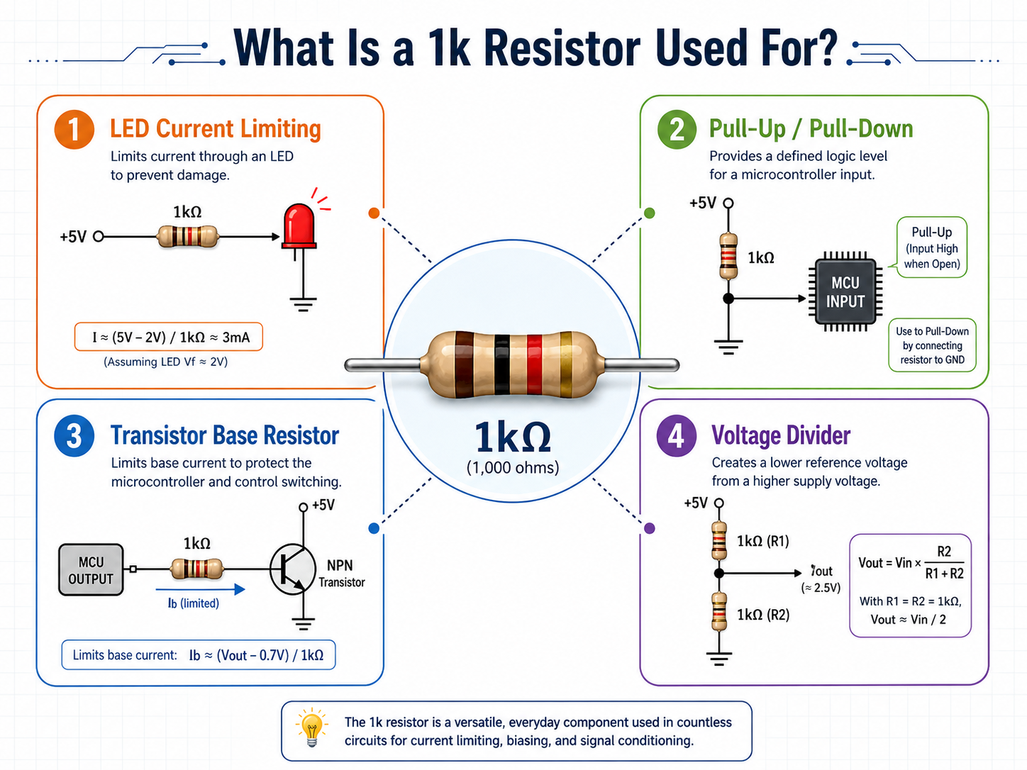
What Is a 1k Ohm Resistor Used For?
A 1k ohm resistor is used in many electronic circuits because it provides a practical current-limiting value for low-voltage designs. It is especially popular in breadboard projects, PCB prototypes, embedded systems, and industrial control boards.
1. LED current limiting
A 1k resistor can limit current through an LED. For example, with a 5V supply and a standard LED, a 1k resistor may allow a small, safe current suitable for indicator lights.
It may not produce maximum brightness, but it is useful when low current consumption is preferred.
2. Pull-up and pull-down circuits
A 1k resistor can help define a digital signal as HIGH or LOW. Pull-up and pull-down resistors prevent floating inputs, which helps microcontrollers read signals more reliably.
In many digital circuits, 1k is considered a stronger pull-up or pull-down value than 10k.
3. Transistor base resistor
A 1k resistor is often used between a microcontroller output and a transistor base. It helps control base current and allows the transistor to switch loads such as LEDs, relays, or small signal circuits.
4. Voltage divider circuits
Two resistors can divide voltage. A 1k resistor may be used with another resistor to create a specific voltage level for analog inputs, reference points, or signal scaling.
5. Signal protection
A 1k resistor can provide simple current limiting for signal lines. It is often placed in series with microcontroller pins, test points, or communication lines to reduce stress during small faults or transitions.
6. PCB testing and debugging
Engineers often use 1k resistors in test circuits because the value is easy to calculate and safe in many low-power conditions.
7. Sensor interface circuits
Some sensors use resistors for biasing, filtering, or signal conditioning. A 1k resistor may be part of a simple RC filter, divider, or output protection path.
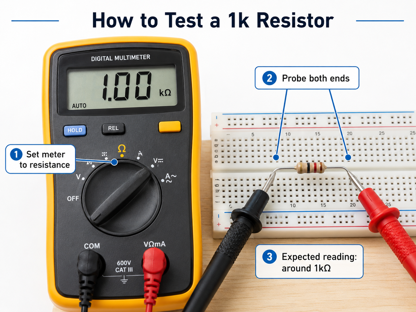
How to Test a 1k Ohm Resistor?
Testing a 1k resistor is simple with a digital multimeter.
Step 1: Turn off circuit power
Before measuring resistance, make sure the circuit is not powered. Resistance mode should not be used on a live circuit.
Step 2: Set the multimeter to resistance mode
Choose the Ω setting. If your meter has manual range selection, choose a range above 1kΩ, such as 2kΩ or 20kΩ.
Step 3: Touch the probes to both ends
Place one probe on each resistor lead or terminal. Polarity does not matter because resistors are non-polar components.
Step 4: Read the value
A normal 1k resistor should read close to 1000Ω.
| Resistor Tolerance | Acceptable Reading Range |
|---|---|
| ±1% | 990Ω to 1010Ω |
| ±2% | 980Ω to 1020Ω |
| ±5% | 950Ω to 1050Ω |
| ±10% | 900Ω to 1100Ω |
Step 5: Consider in-circuit measurement
If the resistor is still soldered on a PCB, other nearby components may affect the reading. For the most accurate result, lift one resistor leg or remove the resistor from the circuit.
For SMD resistors, removal may require hot air, tweezers, or a soldering iron. In professional PCBA repair, technicians often compare the measured value with the schematic and surrounding circuit path.
How Much Current Can a 1k Resistor Handle?
The current a 1k resistor can handle depends mainly on its power rating. The resistance value alone is not enough. You need to know whether the resistor is rated for 1/16W, 1/10W, 1/8W, 1/4W, 1/2W, 1W, or higher.
Two useful formulas are:
Power formula:
P = I²R
Current formula:
I = √(P / R)
For a 1k resistor, the maximum current changes with power rating.
| Power Rating | Approximate Max Current Through 1k Resistor |
|---|---|
| 0.063W / 1⁄16W | 7.9 mA |
| 0.10W / 1⁄10W | 10 mA |
| 0.125W / 1⁄8W | 11.2 mA |
| 0.25W / 1⁄4W | 15.8 mA |
| 0.50W / 1⁄2W | 22.4 mA |
| 1.00W | 31.6 mA |
These are theoretical values at full rated power. In real PCB design, engineers usually leave a safety margin. A resistor running at its full rating may become warm and may have reduced long-term reliability.
Voltage also matters. Using Ohm’s law:
V = I × R
For a 1k resistor:
| Voltage Across Resistor | Current | Power |
|---|---|---|
| 3.3V | 3.3 mA | 0.0109W |
| 5V | 5 mA | 0.025W |
| 12V | 12 mA | 0.144W |
| 24V | 24 mA | 0.576W |
This shows why a 1k resistor works comfortably at 3.3V or 5V in many signal circuits, but may require a higher power rating at 24V.
For example, if a 1k resistor has 24V across it, the power is:
P = V² / R = 24² / 1000 = 0.576W
A small 1/4W resistor would not be suitable for that condition. A higher-rated resistor would be better.
FAQs
1. Is 1k resistor the same as 1000 ohm resistor?
Yes. A 1k resistor is the same as a 1000 ohm resistor. The letter k means kilo, or one thousand. So 1kΩ = 1000Ω.
You may see the same value written as:
- 1k
- 1 kΩ
- 1000Ω
- 1000R
- 1.0K
They all refer to the same resistance value.
2. What is the 4-band color code for a 1k resistor?
The 4-band color code for a 1k resistor is usually:
Brown – Black – Red – Gold
Brown is 1, black is 0, red is the multiplier ×100, and gold means ±5% tolerance.
So:
10 × 100 = 1000Ω
If the tolerance is different, the last band may change. For example, brown as the last band means ±1%, while red means ±2%.
3. What is the 5-band color code for a 1k resistor?
The common 5-band color code for a 1k resistor is:
Brown – Black – Black – Brown – Brown
This means:
- Brown = 1
- Black = 0
- Black = 0
- Brown = ×10
- Brown = ±1% tolerance
So:
100 × 10 = 1000Ω
This type is often used for precision resistors.
4. Can I use a 1k resistor for LED circuits?
Yes, a 1k resistor can be used for many LED circuits, especially as an indicator LED resistor in 3.3V or 5V circuits.
For example, if you use a 5V supply and a red LED with about 2V forward voltage, the resistor has about 3V across it.
Current is:
I = 3V / 1000Ω = 3 mA
This is safe for many small indicator LEDs. The LED may not be extremely bright, but it is usually bright enough for status indication.
For higher brightness, engineers may choose a lower value such as 330Ω or 470Ω, depending on LED rating, supply voltage, and desired current.
5. How do I know if my 1k resistor is damaged?
You can check a 1k resistor with a multimeter. A healthy resistor should measure close to its rated value.
For example:
- ±5% 1k resistor: about 950Ω to 1050Ω
- ±1% 1k resistor: about 990Ω to 1010Ω
A resistor may be damaged if it reads open circuit, far above its rated value, or visually shows burn marks, cracks, discoloration, or damaged leads.
For PCB-mounted resistors, nearby components may affect the reading. If the measured value looks unusual, compare it with the schematic or remove one side of the resistor for a more accurate test.
6. Does resistor tolerance affect 1k resistor value?
Yes. Tolerance tells how much the real value may vary from the marked value.
A 1k resistor with ±5% tolerance can measure between 950Ω and 1050Ω. A 1k resistor with ±1% tolerance can measure between 990Ω and 1010Ω.
For simple LED circuits or general digital circuits, ±5% is often acceptable. For precision measurement, voltage reference, sensor, or analog circuits, ±1% or better may be preferred.