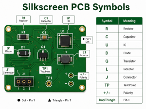
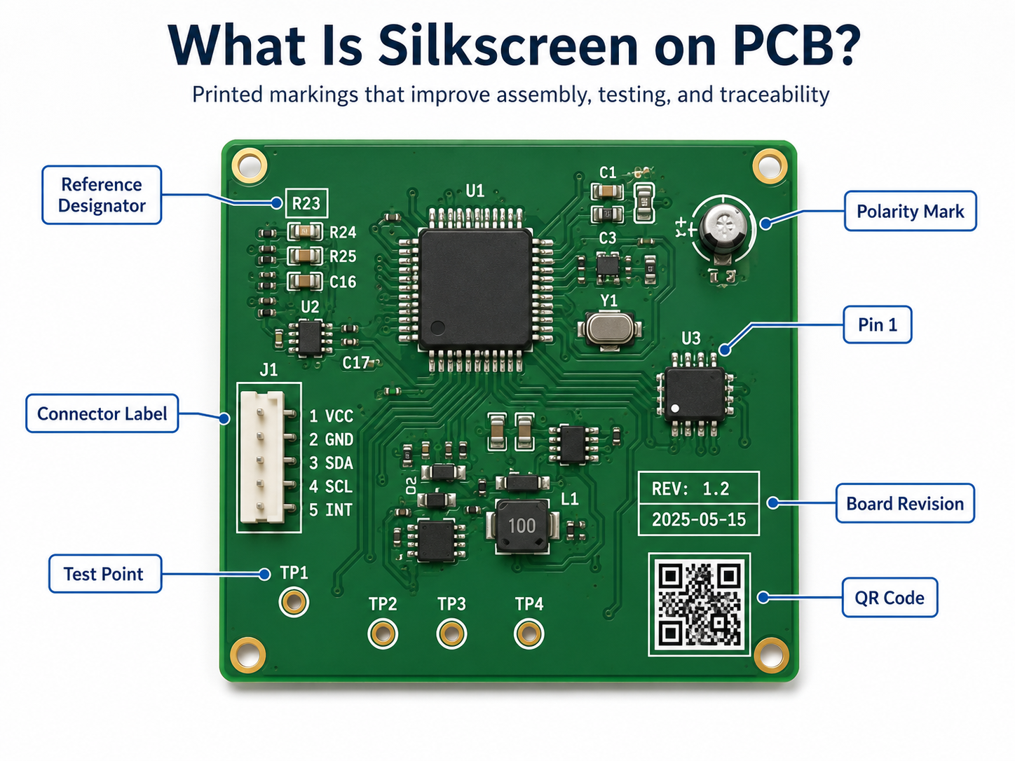
What Is Silkscreen on PCB?
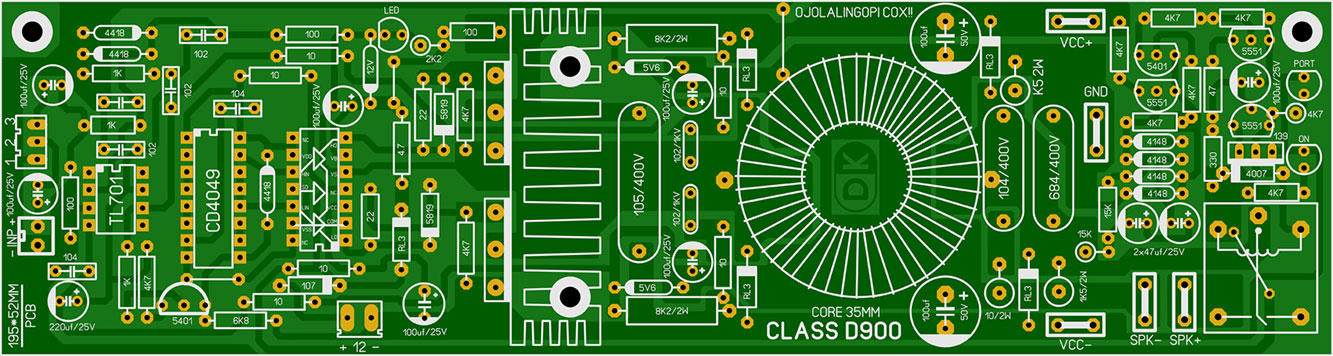
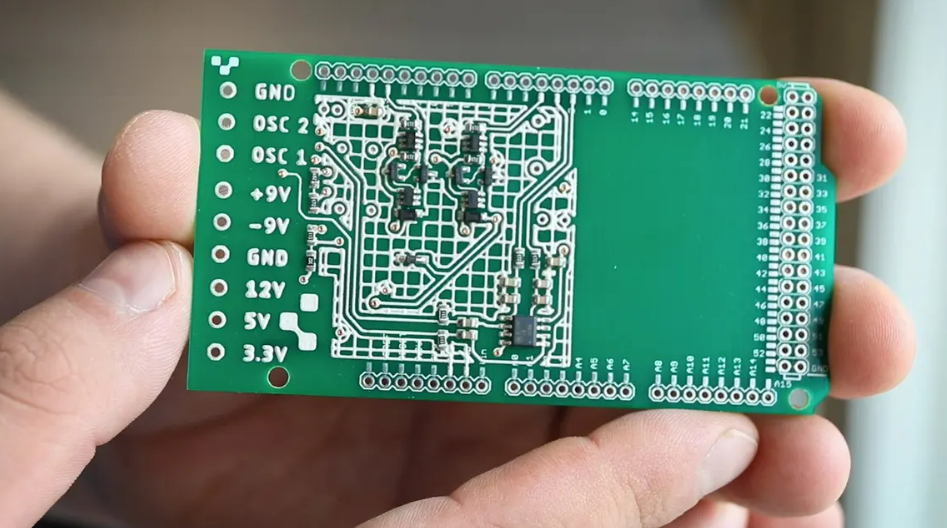
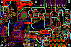
Silkscreen on PCB is the printed layer of text, symbols, logos, reference designators, polarity marks, test points, warning signs, and revision information placed on the surface of a printed circuit board. It does not conduct electricity. Its main job is to help people read, assemble, test, repair, and trace the board more easily.
On most circuit boards, the silkscreen is the white text you see on top of a green solder mask. However, it can also be black, yellow, gray, or another color depending on the PCB surface color and manufacturing process.
What Is the Main Purpose of PCB Silkscreen?
The main purpose of PCB silkscreen is to make the board easier to identify, assemble, inspect, test, and maintain. It gives visible information to people working with the board during production and after the product enters the field.
A good silkscreen design usually includes component names, polarity marks, Pin 1 indicators, connector labels, test point numbers, warning text, board revision, and company logo. These small details can make a large difference during real production.
Common uses include:
- Identifying resistors, capacitors, ICs, diodes, connectors, and switches
- Showing polarity for LEDs, diodes, electrolytic capacitors, and batteries
- Marking Pin 1 on ICs, headers, flat cables, and connectors
- Labeling test points for ICT, flying probe, or functional testing
- Adding board name, part number, revision, date code, or QR code
- Warning users about high voltage, hot surfaces, ESD-sensitive zones, or orientation requirements
- Supporting repair and field maintenance
What Information Should Be Included on a PCB Silkscreen?
A useful PCB silkscreen should include only the information that helps assembly, testing, inspection, traceability, and maintenance. The goal is not to print everything possible. The goal is to print the right information in the right place.
For simple boards, it is common to include every reference designator, such as R1, C1, U1, D1, and J1. For high-density boards, space may be limited, so designers should prioritize information that prevents mistakes.
The most important silkscreen items usually include:
| Silkscreen Item | Example |
|---|---|
| Reference designator | R12, C8, U3, J1 |
| Polarity mark | +, -, cathode line |
| Pin 1 mark | Dot, triangle, “1” |
| Connector label | USB, VIN, OUT, CANH |
| Test point label | TP1, GND, 3V3, RESET |
| Board revision | REV A, V1.2 |
| Manufacturing code | Date code, lot number |
| QR code or serial number | Product ID, batch ID |
| Warning mark | HIGH VOLTAGE, HOT |
| Logo or brand name | EBest, customer logo |
For many products, the highest-priority marks are polarity, Pin 1, connector direction, test points, and board revision. These markings are closely tied to assembly accuracy and maintenance efficiency.
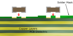
What Is the Difference Between Silkscreen and Solder Mask?
Silkscreen and solder mask are different PCB layers. Solder mask is a protective coating that covers copper and helps control soldering. Silkscreen is a printed marking layer used for text, symbols, logos, and identification.
The solder mask is usually the colored background, such as green, black, blue, red, or white. The silkscreen is the printed legend on top of that surface.
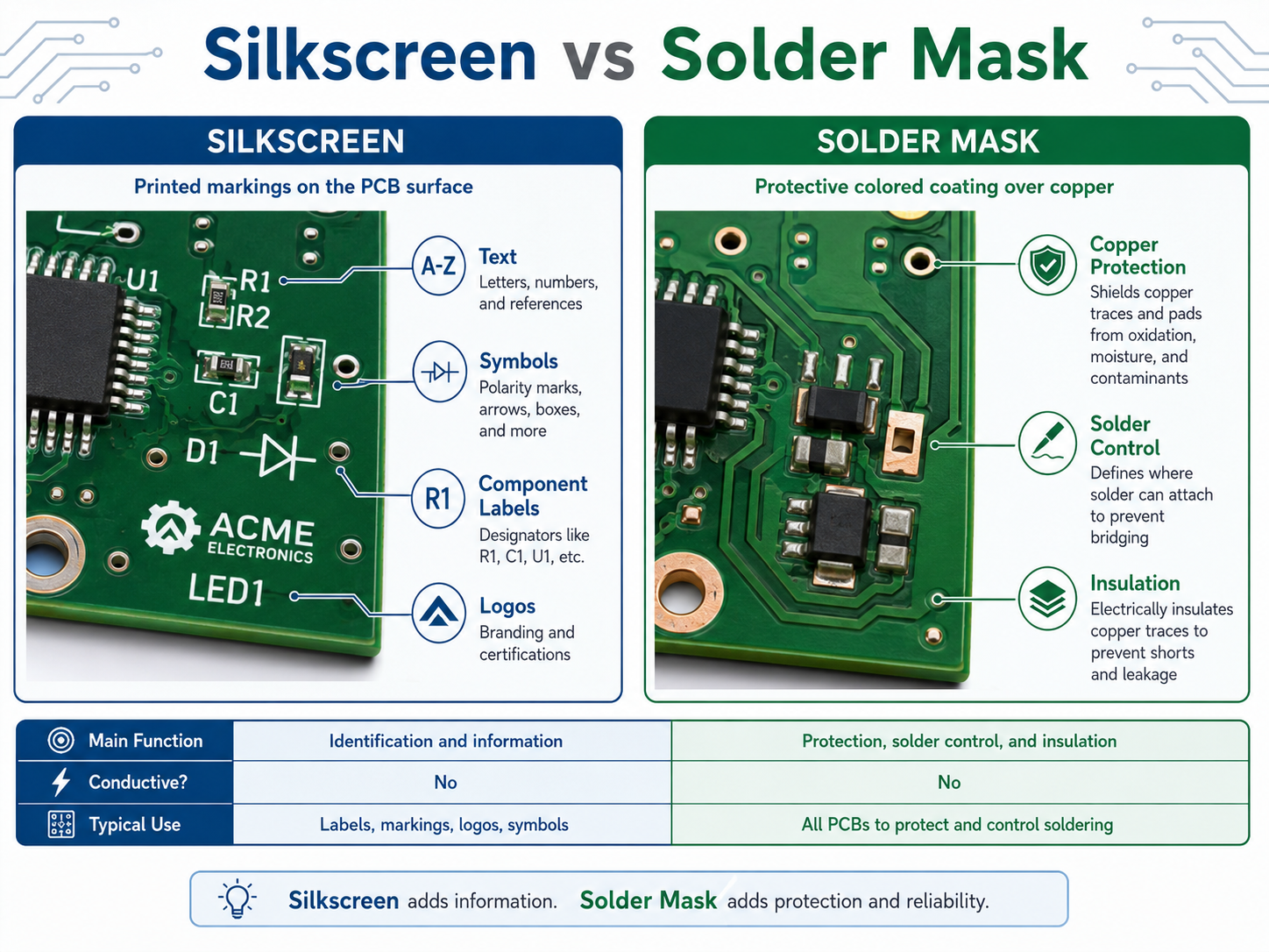
For high-reliability electronics, such as medical devices, industrial controls, aerospace modules, automotive boards, and communication equipment, both layers should be reviewed carefully during DFM checking.
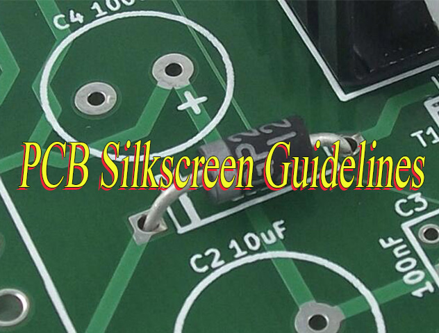
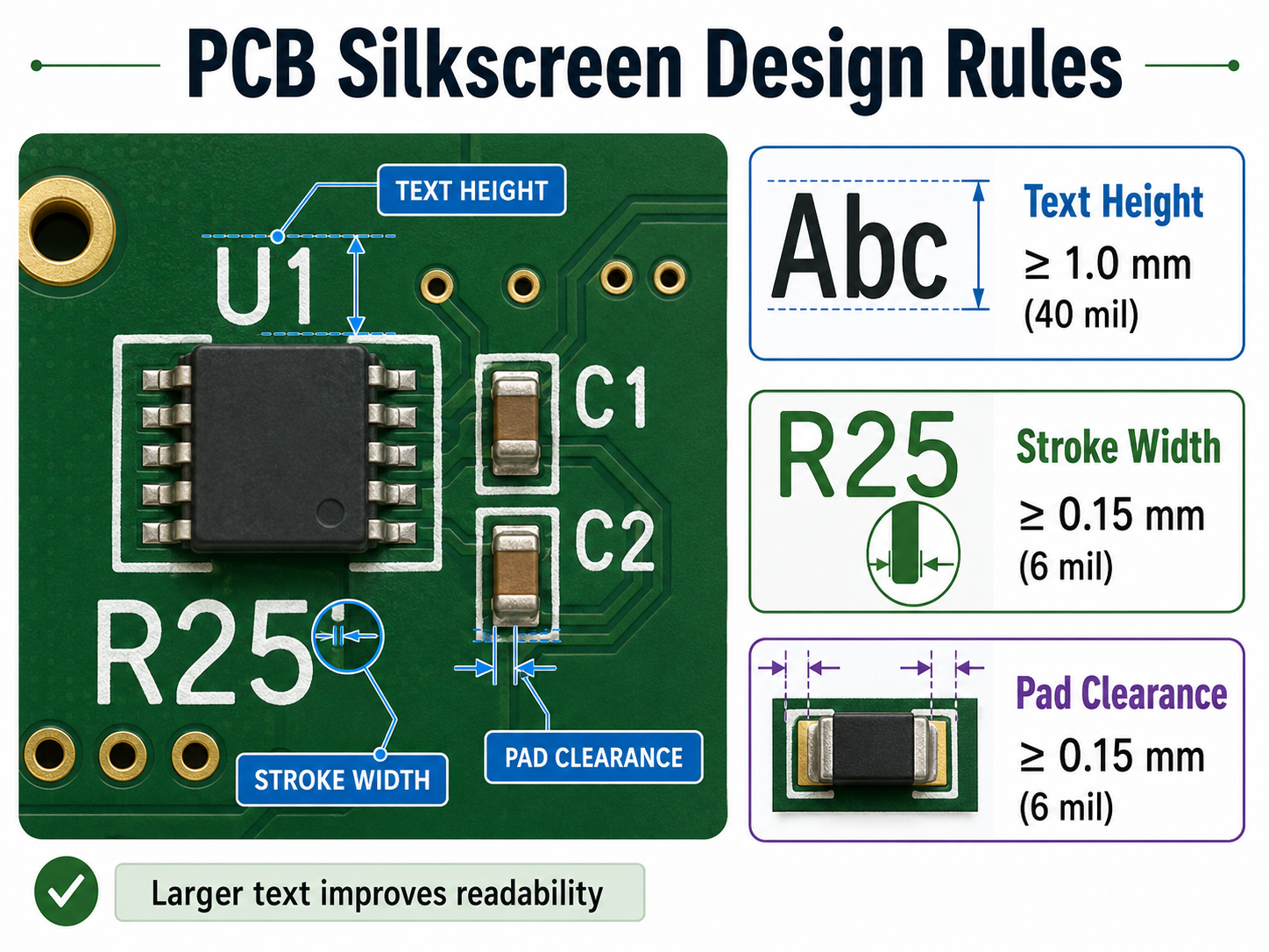
What Are the Standard PCB Silkscreen Design Rules?
Standard PCB silkscreen design rules focus on readability, manufacturability, and clearance. The markings should be large enough to read, thick enough to print, and far enough from pads, exposed copper, and component bodies.
A common mistake is designing silkscreen text that looks clear in CAD software but becomes too small after fabrication. Another common issue is placing text too close to solder pads. During CAM processing, the PCB factory may clip or remove part of the silkscreen to avoid pad contamination.
The following table gives practical reference values for standard PCB projects.
| Design Item | Recommended Value | Better Practice |
|---|---|---|
| Text height | ≥1.0 mm / 40 mil | 1.27 mm / 50 mil |
| Stroke width | ≥0.15 mm / 6 mil | 0.18–0.20 mm / 7–8 mil |
| Clearance to solder pad | ≥0.15 mm / 6 mil | ≥0.20 mm / 8 mil |
| Clearance to exposed copper | ≥0.15 mm / 6 mil | ≥0.20 mm / 8 mil |
| Hollow text height | ≥1.5 mm / 60 mil | ≥2.0 mm / 80 mil |
| Hollow text stroke | ≥0.20 mm / 8 mil | ≥0.25 mm / 10 mil |
| QR code size | Depends on data amount | Confirm with manufacturer |
| Bottom text | Mirrored in layout | Verify in Gerber viewer |
These values are practical for many standard FR4 boards. However, each PCB manufacturer may have different process capability. Fine-pitch HDI boards, ceramic PCBs, metal core PCBs, and high-frequency boards may need a separate review.
What Is the Minimum Text Size for Silkscreen on PCB?
For a reliable and readable PCB silkscreen, a text height of at least 1.0 mm and a stroke width of at least 0.15 mm are commonly recommended. If the board has enough space, larger text is better for manual inspection, testing, and repair.
Here is a useful conversion table for PCB silkscreen design:
| Metric Size | Approx. Imperial Size | Common Use |
|---|---|---|
| 0.15 mm | 5.9 mil | Minimum practical stroke width |
| 0.18 mm | 7.1 mil | More stable stroke width |
| 0.20 mm | 7.9 mil | Better for normal production |
| 0.80 mm | 31.5 mil | Small text, limited readability |
| 1.00 mm | 39.4 mil | Standard readable text height |
| 1.27 mm | 50.0 mil | Better manual readability |
| 1.50 mm | 59.1 mil | Good for labels and warnings |
| 2.00 mm | 78.7 mil | Good for connectors or safety text |
Can Silkscreen Be Printed Over Pads, Vias, or Copper?
Silkscreen should not be printed over solder pads, exposed copper, gold fingers, test pads, or solderable via areas. If the marking overlaps these areas, the factory may remove it during CAM processing. In some cases, poor placement can also affect appearance or assembly readability.
Silkscreen ink is usually non-conductive, but that does not mean it should be placed anywhere. Pads and exposed copper need clean surfaces for soldering, testing, or electrical contact. When silk markings are too close to these areas, the result may be missing text, cut letters, or unclear symbols.
Designers should pay extra attention to these areas:
- SMT pads
- Through-hole pads
- Test points
- Exposed copper zones
- Gold fingers
- Castellated holes
- Thermal pads
- High-current terminals
- RF launch areas
- Fine-pitch IC footprints
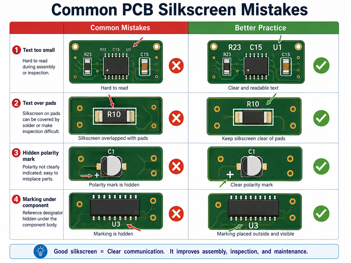
What Are Common PCB Silkscreen Mistakes?
Common PCB silkscreen mistakes include using text that is too small, placing marks under components, printing over pads, forgetting polarity marks, using unclear symbols, and failing to check bottom-side mirroring.
The most common PCB silkscreen mistake including:
What Colors Are Common for PCB Silkscreen?
White is the most common PCB silkscreen color because it gives strong contrast on green, red, blue, and black solder masks. Black silkscreen is common on white solder mask or light-colored boards. Yellow, gray, and other colors may be available depending on the manufacturer.
Color is not only an appearance choice. It affects readability. For example, white text on a green solder mask is easy to read, black text on a white solder mask also gives good contrast. Gray text on a black board may look stylish, but it may be less readable during repair or inspection.
Common color combinations include:
| Solder Mask Color | Common Silkscreen Color | Readability |
|---|---|---|
| Green | White | Excellent |
| Blue | White | Excellent |
| Red | White | Good |
| Black | White | Good |
| White | Black | Excellent |
| Yellow | Black | Good |
| Matte black | White or light gray | Good |
| Transparent / no mask | Depends on copper finish | Requires review |
If the PCB will go through conformal coating, potting, cleaning, or harsh field use, confirm whether the marking remains visible after the final process. The best silkscreen design considers the full product lifecycle, not only the bare board.
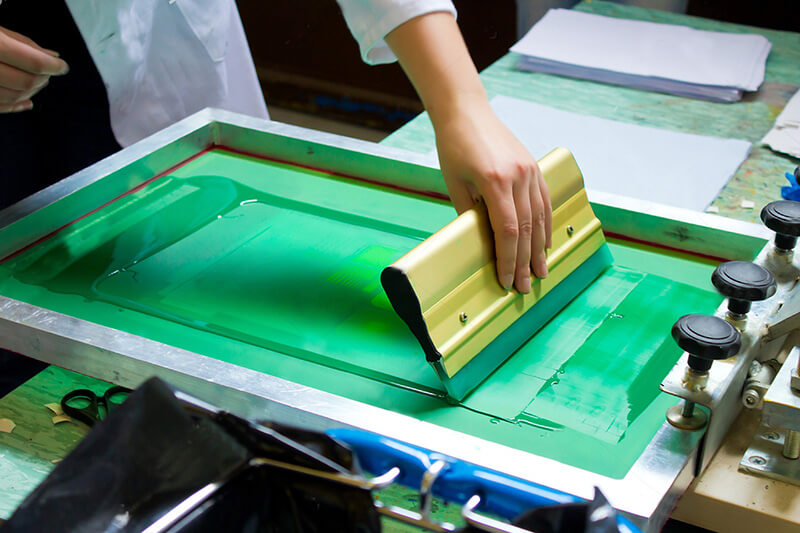
How Can a PCB Manufacturer Improve Silkscreen Quality?
A reliable PCB manufacturer improves silkscreen quality through DFM review, proper printing process selection, CAM checking, readable text control, and clear communication before production. The best result comes from both good design and disciplined manufacturing.
Silkscreen quality depends on several factors:
- Ink type
- Printing method
- Solder mask surface
- Character size
- Stroke width
- Board material
- Surface finish
- Curing process
- CAM clearance rules
- Operator and equipment control
For standard PCBs, traditional silkscreen printing is often sufficient. For dense layouts, QR codes, small text, or high-end appearance, direct legend printing, inkjet printing, or laser marking may be a better option.
EBest Circuit supports PCB fabrication, PCBA assembly, component sourcing, testing, and engineering review for prototype and production projects. For silkscreen-related issues, our team can help check text size, polarity marks, Pin 1 indicators, reference designators, QR code areas, and manufacturing readability before production starts.
How Do You Design Better Silkscreen for High-Density PCBs?
For high-density PCBs, silkscreen should be selective, not crowded. When there is not enough room, keep only the markings that prevent assembly mistakes and support testing. Other information can be moved to the assembly drawing or digital documentation.
A better priority order is:
- Pin 1 marks for ICs and connectors
- Polarity marks for LEDs, diodes, capacitors, and battery connectors
- Test point labels for production and repair
- Connector function labels
- Board revision and traceability marks
- Selected reference designators for important components
- Logo and non-essential graphics
For very small boards, use simple but clear symbols. A small dot for Pin 1, a cathode bar for diode orientation, or a “+” mark for positive polarity can be more valuable than long text.
How Should You Work With a Manufacturer on PCB Silkscreen?
To get a clean silkscreen result, provide complete manufacturing files and ask the PCB manufacturer to review the marking layer before fabrication. This is especially important for dense boards, double-sided assembly, QR code marking, medical electronics, industrial products, and high-reliability applications.
Send these files when possible:
- Gerber files
- Drill file
- PCB stackup
- Assembly drawing
- BOM
- Pick-and-place file
- Special marking requirements
- QR code or serial number rule
- Preferred silkscreen color
- Any customer logo file
- Required board revision format
Before production, confirm these points:
- Is the text size manufacturable?
- Is the stroke width stable?
- Is the silkscreen clear from pads and exposed copper?
- Are Pin 1 and polarity marks visible after assembly?
- Will the QR code scan after printing?
- Is the board revision correct?
- Is bottom-side text mirrored correctly?
- Will coating, cleaning, or final assembly hide any marks?
For customers who need PCB fabrication and assembly together, EBest Circuit can review silkscreen together with component placement, BOM, test access, and assembly process. This helps prevent small marking issues from becoming production delays.
FAQs About Silkscreen on PCB
1. Is silkscreen on PCB necessary?
Yes, it is highly useful. A PCB can work electrically without silkscreen, but clear markings make assembly, testing, inspection, repair, and traceability much easier. For production boards, it is strongly recommended.
2. Does PCB silkscreen affect circuit performance?
In normal designs, it does not affect electrical performance because the ink is non-conductive. Still, it should be kept away from solder pads, exposed copper, RF-sensitive areas, high-voltage clearances, and test contact areas.
3. What is the best font size for PCB silkscreen?
A practical choice is at least 1.0 mm text height with 0.15 mm stroke width. If the board has enough space, 1.27 mm text height and 0.18–0.20 mm stroke width offer better readability.
4. Can I print a logo on PCB silkscreen?
Yes. Logos are commonly printed on PCB silkscreen. The logo should meet minimum line width and spacing rules. It should also avoid pads, exposed copper, QR codes, and important technical markings.
5. Can silkscreen include QR codes or serial numbers?
Yes. QR codes, serial numbers, lot codes, and product IDs can be added to support traceability. For small or high-density codes, laser marking or high-resolution printing may be more reliable than standard silkscreen.
6. Why did some silkscreen text disappear after PCB production?
The most common reason is that the text overlapped pads, vias, exposed copper, or restricted areas. During CAM processing, the factory may remove part of the marking to protect solderability and manufacturing quality.
7. What is the difference between PCB silkscreen and PCB legend?
They usually refer to the same idea. “Silkscreen” often describes the printed marking process, while “legend” refers to the text and symbols shown on the PCB surface.
8. Which silkscreen color is best for PCB?
White is the most common choice because it works well on green, blue, red, and black solder masks. Black is better for white solder mask. The best color is the one that gives strong contrast and stable readability.
Conclusion
Silkscreen on PCB may look like a small detail, but it has a practical role in the full product lifecycle. It helps assemblers place components correctly, helps testers find signals quickly, helps repair teams locate parts, and helps manufacturers support traceability.
EBest Circuit provides PCB fabrication, PCBA assembly, component sourcing, DFM review, and testing support for prototype and mass production projects. If your PCB needs clear silkscreen, reliable assembly, and traceable production, send your Gerber and BOM files to our team for review.
Contact EBest Circuit: sales@bestpcbs.com