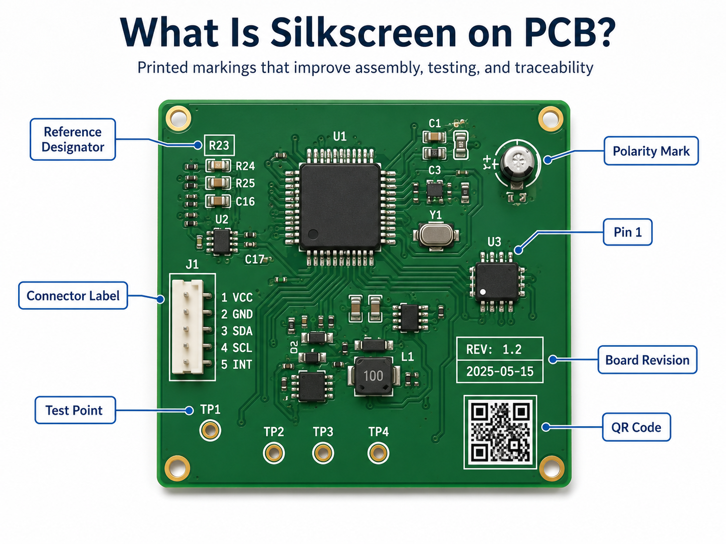
What Is Silkscreen on PCB?
Silkscreen on PCB is the printed marking layer used to show component names, polarity marks, Pin 1 indicators, test points, logos, warning labels, QR codes, and board revision information. It helps engineers, assemblers, inspectors, and repair technicians understand the PCB faster.
This layer is also called the PCB legend layer or component marking layer. It does not carry current, but it plays a practical role in assembly accuracy, testing efficiency, repair work, and product traceability.
Why Is Silkscreen Important on a PCB?
PCB silkscreen is important because it turns a bare circuit board into a readable engineering document. Without silkscreen, the board may still work electrically, but assembly, inspection, testing, and repair become slower.
Clear markings help identify resistors, capacitors, ICs, connectors, test points, power input, signal direction, and safety warnings. In production, a clean silkscreen can reduce orientation mistakes, shorten debugging time, and improve communication between PCB design, fabrication, and assembly teams.
What Is Silkscreen PCB Material?
Silkscreen PCB material usually refers to the ink or marking medium used to print text, symbols, and graphics on the PCB surface. The most common material is non-conductive epoxy ink or UV-curable ink. These materials are selected because they can bond to solder mask, resist normal handling, and remain readable after PCB fabrication.
In standard PCB manufacturing, silkscreen material must be compatible with solder mask color, curing temperature, surface finish, cleaning process, and assembly environment. For more demanding products, such as industrial electronics, automotive modules, medical PCBs, or outdoor devices, the marking material should also offer better resistance to abrasion, chemicals, humidity, and temperature changes.
What Are the Common Types of Silkscreen PCB Material?
Different silkscreen PCB material options are used depending on cost, readability, board density, and traceability requirements. Standard epoxy ink is common for most FR4 PCBs. UV-curable ink is used when faster curing and sharper printing are needed. Laser marking is often selected for QR codes, serial numbers, and durable traceability marks.
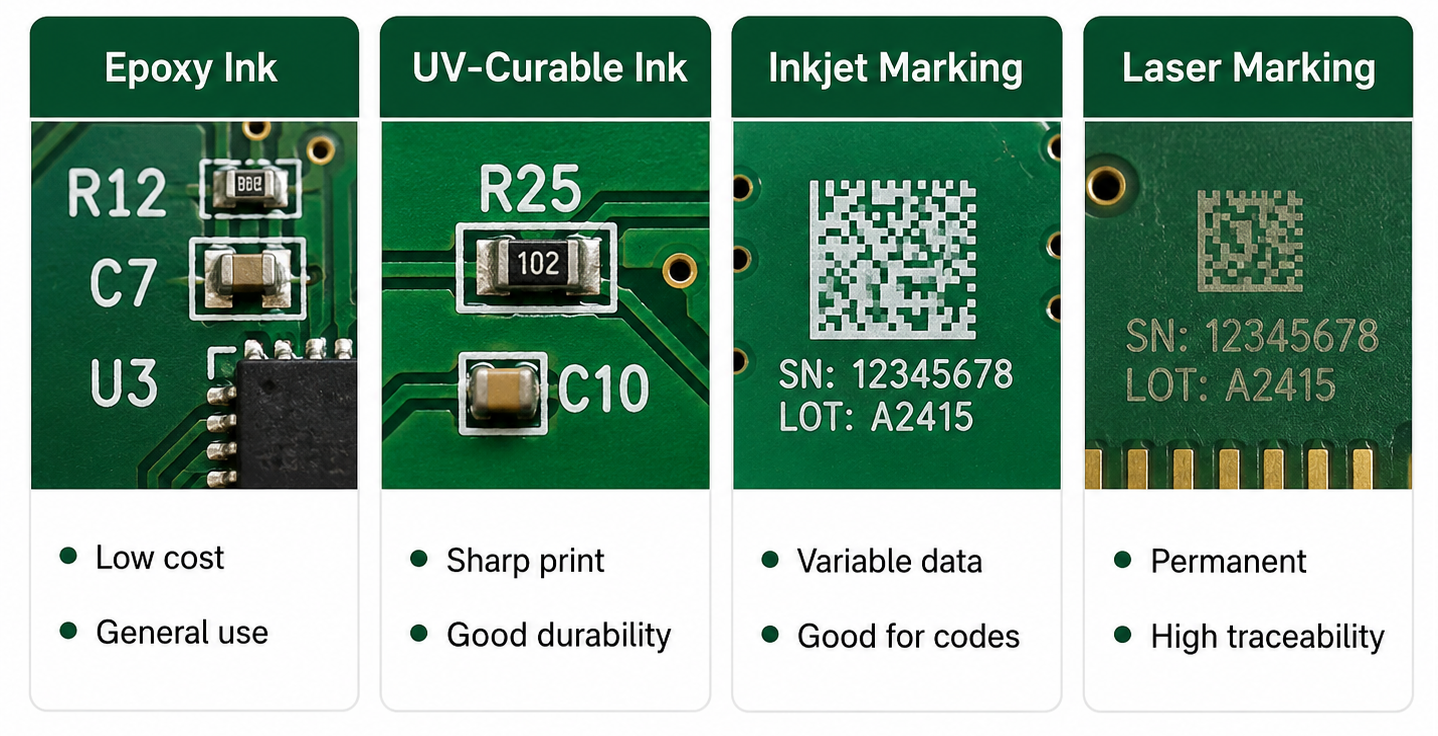
For general PCB projects, standard white epoxy or UV ink is enough. For small text, QR codes, high-density boards, or products requiring long-term traceability, higher-resolution printing or laser marking may be a better choice.
How Does Silkscreen PCB Material Affect Readability and Durability?
Silkscreen PCB material affects how sharp, visible, and durable the printed markings are. A good material should keep letters clear after curing, cleaning, soldering, handling, and final assembly.
If the ink spreads too much, small characters may look blurry. If the ink adhesion is weak, markings may fade or scratch off. If the color contrast is poor, technicians may struggle to read the board during inspection or repair.
For example, white silkscreen on green solder mask is easy to read. Black silkscreen on white solder mask also gives strong contrast. But low-contrast combinations, such as gray text on black solder mask, may look stylish while reducing practical readability.
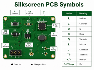
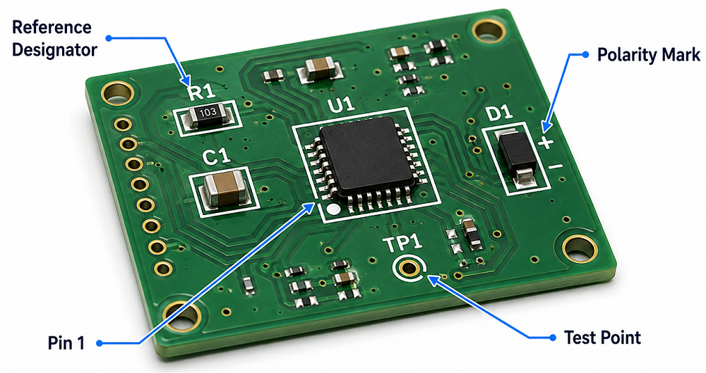
What Are Silkscreen PCB Symbols?
Silkscreen PCB symbols are printed marks used to identify components, polarity, Pin 1 direction, test points, connectors, warning areas, and functional zones on a circuit board. These symbols help users understand the board without opening the schematic every time.
Common silkscreen PCB symbols include “+” and “-” for polarity, dots or triangles for Pin 1, diode bars for cathode direction, TP labels for test points, and reference designators such as R, C, U, D, J, L, Q, and F.
What Do Common Silkscreen PCB Symbols Mean?
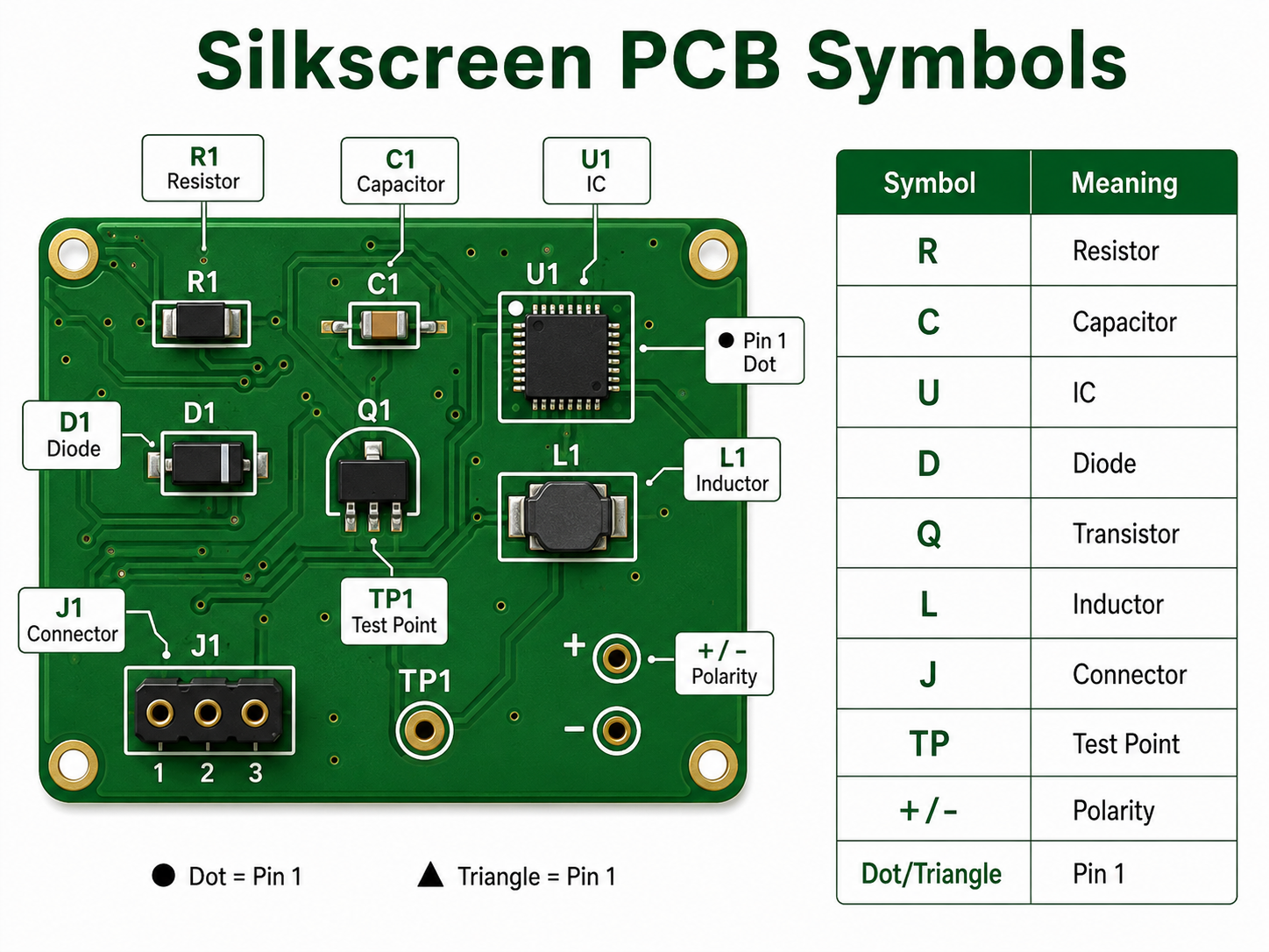
| Silkscreen PCB Symbol | Meaning | Example |
|---|---|---|
| R | Resistor | R1, R25 |
| C | Capacitor | C3, C18 |
| U / IC | Integrated circuit | U1, IC2 |
| D | Diode or LED | D5, LED1 |
| Q | Transistor or MOSFET | Q2, Q10 |
| L | Inductor | L1, L4 |
| J / CN | Connector | J1, CN3 |
| F | Fuse | F1 |
| TP | Test point | TP1, TP_GND |
| SW | Switch | SW1 |
| + / – | Polarity | Capacitor, battery, LED |
| Dot / triangle / “1” | Pin 1 indicator | IC or connector orientation |
| GND | Ground | Ground test point |
| VIN / VOUT | Power input/output | Power connector marking |
| HV | High voltage warning | Power supply board |
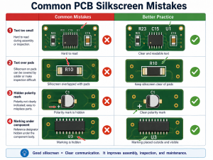
These silkscreen PCB symbols are small, but they carry important information. A missing polarity mark or unclear Pin 1 indicator can cause assembly errors, especially on LED boards, power supplies, sensor modules, and control boards.
How Do Silkscreen PCB Symbols Help Assembly?
Silkscreen PCB symbols help assembly teams place and inspect components correctly. They show where each component belongs, which direction it should face, and how connectors or test points should be used.
For SMT assembly, symbols such as Pin 1 dots, diode direction marks, and capacitor polarity marks are very useful during first article inspection. For through-hole assembly, connector names, switch labels, and power marks help manual operators avoid wrong insertion.
In PCBA production, clear symbols can support:
- Faster visual inspection
- Lower risk of component orientation errors
- Easier connector installation
- Better manual soldering guidance
- Faster functional testing
- Easier repair and troubleshooting
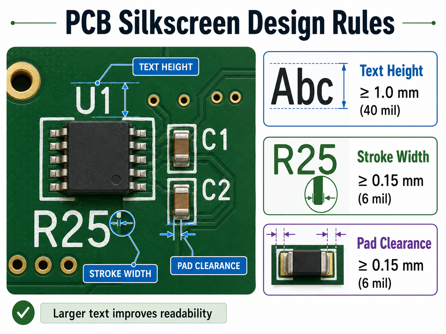
What Are the Design Rules for Silkscreen on PCB?
Silkscreen on PCB should be designed with enough character size, stroke width, and clearance from pads. The markings must remain readable after fabrication and assembly.
| Design Item | Recommended Value |
|---|---|
| Text height | ≥1.0 mm / 40 mil |
| Stroke width | ≥0.15 mm / 6 mil |
| Clearance to pads | ≥0.15 mm / 6 mil |
| Clearance to exposed copper | ≥0.15 mm / 6 mil |
| Hollow font height | ≥1.5 mm / 60 mil |
| QR code size | Confirm with supplier |
| Bottom-side text | Mirrored correctly |
If the board is very dense, do not force every component label onto the PCB. Keep important markings first: Pin 1, polarity, test points, connector names, warning labels, and revision number.
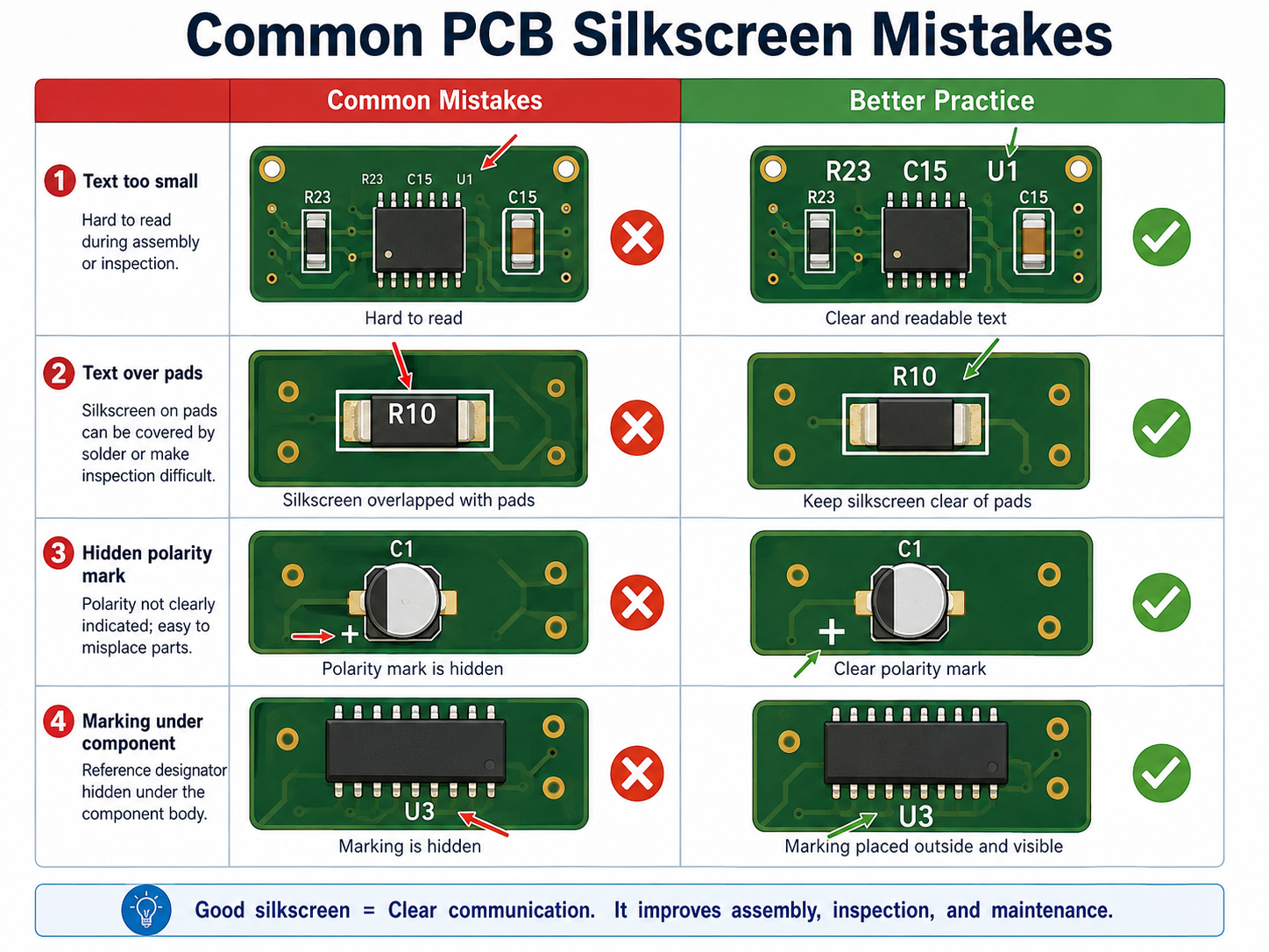
Can Silkscreen Be Printed Over Pads or Vias?
Silkscreen should not be printed over solder pads, exposed copper, gold fingers, test points, or solderable vias. If silkscreen overlaps these areas, the PCB manufacturer may remove part of the text during CAM processing.
This is why some letters disappear after fabrication. The original design may show complete text, but the manufacturing file may clip it to protect soldering quality.
A better practice is to place reference designators outside component bodies and away from pads. For small components, use shorter labels or place the full reference information in the assembly drawing.
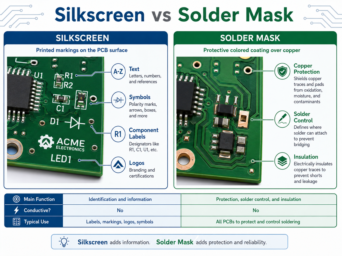
What Is the Difference Between Silkscreen PCB Material and Solder Mask Material?
Silkscreen PCB material is used for printed markings. Solder mask material is used to protect copper and prevent solder bridges. They are different layers with different functions.
| Item | Silkscreen PCB Material | Solder Mask Material |
|---|---|---|
| Main function | Prints text, symbols, and logos | Covers and protects copper |
| Electrical role | Non-conductive marking | Insulating protection |
| Common color | White, black, yellow | Green, black, blue, red, white |
| Used for | Component labels, symbols, warnings | Solder control and copper protection |
| Design concern | Readability and clearance | Insulation and solderability |
A PCB needs solder mask for manufacturing protection. Silkscreen is used for human readability. Both layers support production quality, but they should not be confused.
How Should You Choose Silkscreen PCB Material and Color?
Choose silkscreen PCB material and color based on readability, product environment, board density, and traceability needs. For most PCB projects, white silkscreen on green solder mask is the safest and most readable choice.
For white solder mask, black silkscreen is usually better. For black solder mask, white silkscreen gives better contrast. For products with QR codes, serial numbers, or long-term tracking needs, laser marking or high-resolution legend printing may be more reliable.
| PCB Solder Mask Color | Recommended Silkscreen Color | Readability |
|---|---|---|
| Green | White | Excellent |
| Blue | White | Excellent |
| Red | White | Good |
| Black | White | Good |
| White | Black | Excellent |
| Yellow | Black | Good |
For industrial, medical, automotive, and communication products, readability should be more important than visual decoration. A beautiful board is helpful, but a readable board is more useful in production and maintenance.
How Can EBest Circuit Help With PCB Silkscreen Design and Manufacturing?
EBest Circuit can help review silkscreen on PCB before fabrication and assembly. Our team checks text size, symbol clarity, polarity marks, Pin 1 indicators, pad clearance, QR code position, and board revision information during DFM review.
This is especially useful for turnkey PCB and PCBA projects. Silkscreen is not only a printing detail. It connects with BOM verification, component orientation, assembly inspection, testing, traceability, and repair documentation.
EBest Circuit supports:
- PCB fabrication
- PCBA assembly
- Component sourcing
- Free DFM review
- Silkscreen readability check
- QR code and serial number marking
- AOI, X-ray, ICT, and functional testing
- Prototype to mass production support
For projects that require clean markings, stable assembly, and traceable manufacturing, send your Gerber and BOM files to sales@bestpcbs.com.
FAQs
1. What is silkscreen on PCB?
Silkscreen on PCB is the printed marking layer that shows component names, symbols, polarity, test points, logos, QR codes, and board revision information. It helps people assemble, test, inspect, and repair the PCB more easily.
2. What material is used for PCB silkscreen?
Common silkscreen PCB material includes epoxy-based ink, UV-curable ink, LPI legend ink, inkjet marking ink, or laser marking depending on the required precision, durability, and traceability.
3. What do silkscreen PCB symbols mean?
Silkscreen PCB symbols identify components and board functions. For example, R means resistor, C means capacitor, U means IC, D means diode, TP means test point, and “+ / -” shows polarity.
4. Does silkscreen PCB material affect circuit performance?
Normally, no. Silkscreen material is non-conductive and does not carry current. However, poor placement over pads, exposed copper, or sensitive areas can create manufacturing or readability problems.
5. Can PCB silkscreen symbols be customized?
Yes. Custom symbols, logos, connector labels, warning marks, QR codes, and product IDs can be printed on the PCB as long as they meet the manufacturer’s minimum size and clearance rules.
6. What is the best silkscreen color for PCB?
White is the most common silkscreen color because it gives strong contrast on green, blue, red, and black solder mask. Black silkscreen is usually better for white solder mask.