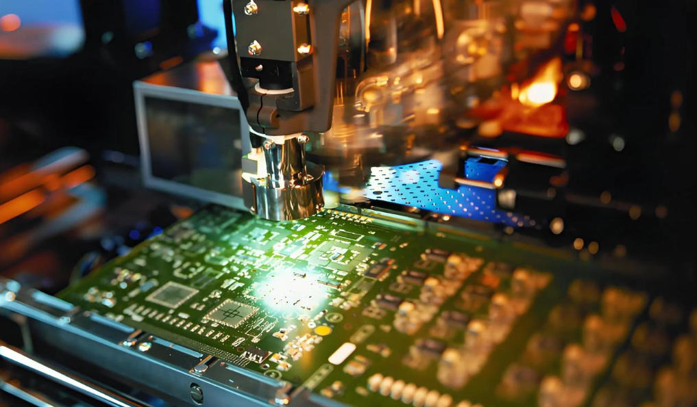
Can the right PCB layout tips turn a problematic circuit design into a reliable high-performance system? Many circuit designs fail not because of flawed schematics but improper layout choices that compromise signal integrity, power stability, and thermal management. This guide breaks down actionable PCB layout tips and techniques to avoid common pitfalls, enhance performance, and ensure compliance all tailored to address the real-world challenges faced in circuit design.
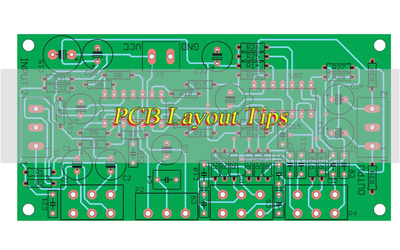
What Are the Essential PCB Layout Tips for Beginners to Avoid Common Mistakes?
Beginners often overlook basic layout principles that lead to costly reworks and performance issues. The following PCB layout tips focus on foundational, actionable practices to prevent common errors and set a strong base for any design.
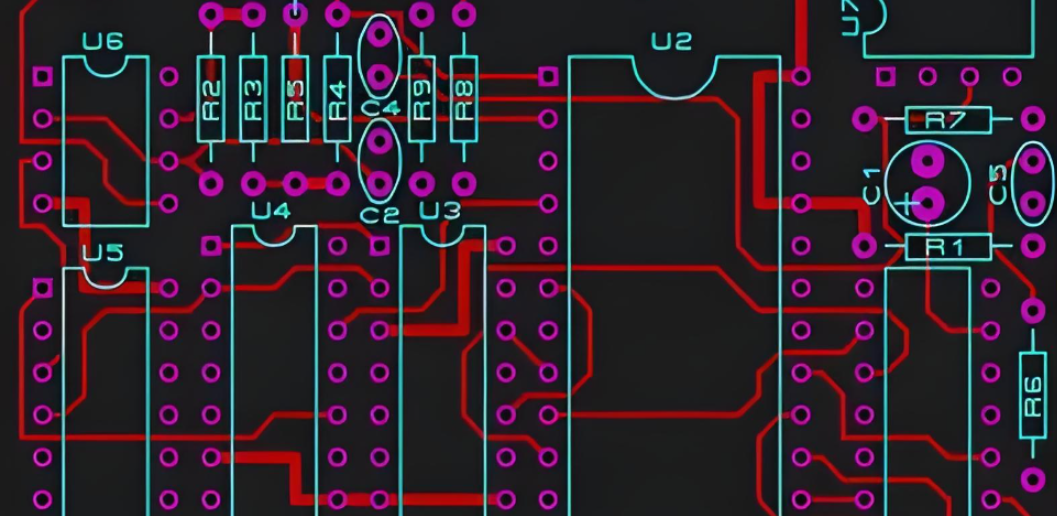
- Match Component Footprints to Datasheets: Always cross-verify component footprints with manufacturer datasheets. Use the exact footprint provided by the component manufacturer never guess or modify footprints without confirmation. For example, confusing 0603 (1.6mm x 0.8mm) and 0805 (2.0mm x 1.25mm) resistors will cause soldering bridges or poor connections. For QFN components, double-check pad size, pitch, and thermal pad dimensions, as misalignment leads to thermal and electrical failures. Always confirm footprint compatibility with your PCB design software before finalizing.
- Keep Power and Ground Traces Separate from Signal Traces: Avoid routing power or ground traces alongside sensitive signal traces (e.g., analog sensors, low-voltage signals). Power traces carry varying currents that generate noise, which disrupts signal quality. Maintain a minimum spacing of 2–3 mils between power/ground traces and signal traces. Ensure power traces are sufficiently wide use 10 mils for 1A, 20 mils for 2A, and 30 mils for 3A to handle current demands without voltage drops or overheating.
- Place Decoupling Capacitors Correctly: Decoupling capacitors filter out power supply noise and stabilize voltage for integrated circuits. Place them within 5–10 mils of the IC’s power pins, with traces no longer than 15 mils to both power and ground. Use a combination of 0.1µF (for high-frequency noise) and 1µF (for low-frequency noise) capacitors for each IC power pin. Avoid daisy-chaining decoupling capacitors each IC should have its own dedicated decoupling to ensure fast response to voltage fluctuations.
- Avoid Overcrowding Components: Overcrowding leads to poor heat dissipation, difficult soldering, and increased signal crosstalk. Leave a minimum of 10 mils between passive components (resistors, capacitors) and 20 mils between active components (ICs, transistors). For power components (MOSFETs, voltage regulators), leave 30–50 mils of spacing to promote airflow. Follow manufacturer recommendations for minimum component spacing, and use a 3D view in your design software to check for physical collisions.
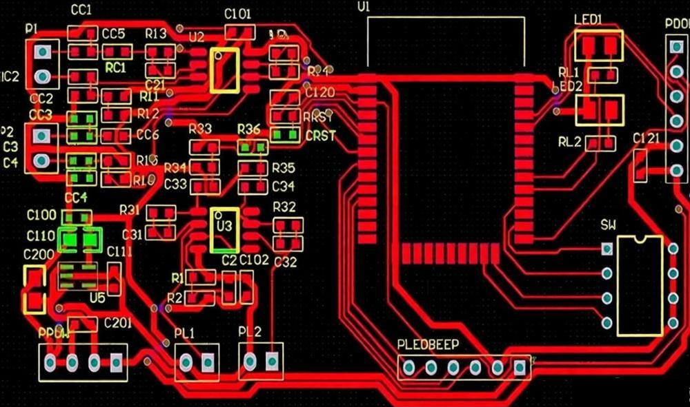
- Plan Trace Routing Before Starting: Map out trace paths before routing to avoid unnecessary bends, loops, or crossings. Use shorter, straighter traces keep critical signal traces under 1 inch where possible to reduce signal delay and attenuation. For multi-layer PCBs, assign dedicated layers for power, ground, analog signals, and digital signals in advance. Use a netlist to group related signals, and route power and ground traces first before moving to signal traces.
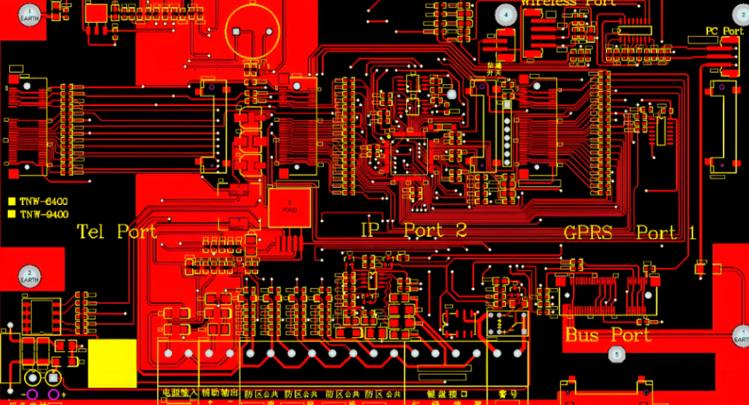
- Label Components and Nets Clearly: Add clear labels to all components (e.g., R1, C1, U1) and nets (e.g., VCC_3.3V, GND, I2C_SDA) to simplify assembly and troubleshooting. Use a consistent labeling format, and place labels in open areas of the PCB where they are easily visible. Avoid placing labels over traces or pads, as this can interfere with soldering or signal integrity.
How to Apply Practical PCB Layout Tips and Tricks to Enhance Signal Integrity?
Signal integrity ensures signals travel from source to load without distortion a critical factor for circuit performance. These PCB layout tips focus on reducing noise, crosstalk, and reflection to maintain signal quality, with actionable steps for every design.
- Control Trace Impedance: Match trace impedance to the source and load impedance (typically 50 ohms for most signals, 100 ohms for differential signals) to minimize signal reflection. Use an impedance calculator to determine trace width, spacing, and dielectric thickness based on your PCB material (e.g., FR-4 with 1oz copper). For a 50-ohm trace on FR-4 (1.6mm thick), use a 50-mil width for a single-ended trace. Maintain consistent impedance across the entire trace avoid sudden changes in width or spacing.
- Minimize Trace Length and Bends: Shorter traces reduce signal delay and attenuation. Keep high-frequency signals (above 50 MHz) under 2 inches where possible. Avoid sharp 90-degree bends, which cause impedance changes and signal reflection. Use 45-degree bends or rounded corners (with a radius equal to the trace width) instead. For traces that must be long, add a series resistor (10–100 ohms) near the source to reduce reflection.
- Separate High-Speed and Low-Speed Signals: High-speed signals (e.g., USB, HDMI, Ethernet) generate electromagnetic interference that disrupts low-speed signals (e.g., analog sensors, UART). Route high-speed traces in a dedicated area, at least 50 mils away from low-speed traces. Use ground planes to isolate high-speed traces place a ground trace on both sides of high-speed traces for additional shielding. Avoid routing high-speed traces over gaps in the ground plane.
- Use Ground Planes for Signal Return Paths: A solid ground plane provides a low-impedance return path for signals, reducing noise and crosstalk. Ensure signal traces run directly above the ground plane to minimize loop area (critical for high-frequency signals). Use a single continuous ground plane avoid splitting the ground plane, as this creates discontinuities in the return path and increases noise. For multi-layer PCBs, place the ground plane between signal layers for maximum shielding.
- Implement Differential Pair Routing: For differential signals (e.g., USB 3.0, HDMI, Ethernet), route traces in pairs with equal length, spacing, and impedance. Keep the pair parallel throughout the route maintain a spacing of 5–10 mils between the two traces. Ensure both traces have the same length (within ±1 mil) to avoid skew. Avoid crossing other traces or changing layers unnecessarily; if layer changes are required, use vias for both traces at the same location.
- Avoid Stubs on High-Speed Traces: Stubs (short, unused segments of trace) on high-speed signals cause signal reflection and degradation. Keep stubs under 5 mils in length if longer stubs are unavoidable, use a termination resistor at the end of the stub. For example, a stub longer than 10 mils on a 100 MHz signal can cause significant reflection and signal loss.
What PCB Layout Design Tips Should Engineers Follow for High-Speed Circuits?
High-speed circuits (operating above 100 MHz) require specialized layout techniques to handle signal propagation effects and noise. These PCB layout tips address the unique challenges of high-speed design to ensure reliable performance, with practical steps for implementation.
- Maintain Equal Trace Lengths for Critical Signals: For bus signals (e.g., DDR memory, PCIe), ensure all traces in the bus have the same length to prevent skew. Skew occurs when signals arrive at the load at different times, causing data errors. Use length matching tools in your design software to adjust trace lengths within a tolerance of ±5 mils. For DDR4 memory, keep clock and data traces within 10 mils of each other in length. Add serpentine traces (with minimal bends) to adjust lengths without increasing noise.
- Reduce Parasitic Inductance and Capacitance: Parasitic elements (inductance from long traces, capacitance from adjacent traces) degrade high-speed signal quality. Minimize trace length keep high-speed traces under 1.5 inches where possible. Keep traces at least 20 mils away from each other to reduce parasitic capacitance. Use shorter vias (preferably 0.3mm diameter) to reduce parasitic inductance. Avoid placing traces over gaps in the ground plane, as this increases parasitic capacitance and signal reflection.
- Isolate Clock Signals: Clock signals are high-frequency and generate significant noise. Route clock traces in a dedicated layer, surrounded by ground traces (10–15 mils spacing) or a ground plane, to isolate them from other signals. Keep clock traces as short as possible under 1 inch for clocks above 200 MHz. Avoid routing clock traces near sensitive components (e.g., analog sensors, voltage regulators) and avoid crossing clock traces with other high-speed signals.
- Use Blind and Buried Vias: Blind vias (connecting the top layer to inner layers) and buried vias (connecting inner layers) reduce trace length and minimize signal reflection in high-speed circuits. They also save space on the PCB surface, allowing for more compact designs without sacrificing performance. Use blind vias for signal traces that need to connect to inner layers, and buried vias for power and ground connections between inner layers. Ensure via size is compatible with your manufacturer’s capabilities (typically 0.2–0.4mm diameter).
- Implement Signal Termination: Add termination resistors to high-speed signal lines to match impedance and reduce reflection. Use series termination (a resistor placed near the source) for point-to-point signals choose a resistor value equal to the trace impedance (e.g., 50 ohms for 50-ohm traces). Use parallel termination (a resistor placed near the load) for bus signals connect the resistor to ground or VCC, depending on the signal type. Follow manufacturer guidelines to place termination resistors as close to the source or load as possible (within 5–10 mils).
- Use a Dedicated Power Plane for High-Speed ICs: High-speed ICs (e.g., microcontrollers, FPGAs) require clean power to maintain performance. Use a dedicated power plane for these ICs, separate from other power supplies. Add additional decoupling capacitors (0.1µF, 1µF, and 10µF) near the IC’s power pins to filter out high-frequency noise. Ensure the power plane is connected to the ground plane via multiple vias to reduce impedance.
What Are the PCB Board Layout Tips to Ensure Stable Power Distribution?
Stable power distribution is essential for consistent circuit performance, as voltage fluctuations or noise can cause component failure or incorrect operation. These PCB layout tips focus on delivering clean, stable power to all components, with actionable steps for every design.
- Use Adequately Sized Power Traces: Power traces must handle the maximum current of the circuit without voltage drop or overheating. Calculate trace width using a trace width calculator account for current, copper thickness (1oz = 35µm), PCB material, and ambient temperature. A general guideline: 10 mils for 1A, 20 mils for 2A, 30 mils for 3A, and 50 mils for 5A. For currents above 5A, use a power plane instead of traces to reduce resistance and heat.
- Implement a Power Plane in Multi-Layer PCBs: A dedicated power plane provides a low-impedance path for power distribution, reducing noise and voltage drops. The power plane should cover the entire PCB area where possible, ensuring uniform power delivery to all components. Pair the power plane with a ground plane (adjacent layer) to minimize loop area and reduce noise. For multiple power supplies (e.g., 3.3V, 5V), use separate power planes to prevent cross-contamination.
- Place Bulk Capacitors Near Power Inputs: Bulk capacitors (e.g., 10µF, 100µF, 220µF) filter low-frequency noise and stabilize the main power supply. Place them within 1 inch of the power input connector to smooth voltage fluctuations and provide instantaneous current during peak demand. Use tantalum or ceramic capacitors for bulk storage tantalum capacitors have higher capacitance density, while ceramic capacitors have faster response times. Add at least one bulk capacitor per power supply input.
- Separate Power Supplies for Different Circuit Sections: If the circuit uses multiple power supplies (e.g., 3.3V for digital, 5V for analog, 12V for power components), separate their power traces and planes to prevent cross-contamination. Use separate voltage regulators for each supply to ensure stable voltage levels. Route analog power traces away from digital power traces maintain a minimum spacing of 50 mils. Connect all power grounds to a single common ground point to avoid ground loops.
- Avoid Power Trace Loops: Power trace loops create magnetic fields that generate noise and interfere with signal integrity. Keep power traces as straight as possible and avoid forming loops. Use the power plane to provide a direct path from the supply to components avoid routing power traces in a circular path. For power traces that must turn, use 45-degree bends and keep the loop area as small as possible.
- Add Fuses or Polyfuses for Overcurrent Protection: Include fuses or polyfuses in the power path to protect components from overcurrent. Place fuses near the power input connector, before any other components. Choose a fuse rating 1.2–1.5 times the maximum current of the circuit this ensures the fuse blows only during overloads. Use polyfuses for resettable protection, which automatically recover after the overload is removed.
How Do PCB Layout Techniques Differ Between Analog and Digital Circuit Designs?
Analog and digital circuits have distinct characteristics analog circuits handle continuous signals and are sensitive to noise, while digital circuits handle discrete signals and generate more noise. These PCB layout tips highlight the key differences in layout techniques for each type, with practical steps to optimize both.
- Component Placement: For analog circuits, place sensitive components (e.g., op-amps, sensors, ADCs) away from noise sources (e.g., oscillators, digital ICs, power components) by at least 50 mils. Group analog components by function (e.g., signal conditioning, amplification) to minimize trace length and reduce noise. For digital circuits, place components to minimize signal delay group high-speed components (e.g., microcontrollers, memory) together, within 1–2 inches of each other. Avoid placing digital components near analog sensors or op-amps.
- Grounding Techniques: Analog circuits require a single-point ground to avoid ground loops, which cause noise. Connect all analog ground points (e.g., op-amp grounds, sensor grounds) to a single node before connecting to the main ground. Use a separate analog ground plane for sensitive analog circuits. Digital circuits can use a multi-point ground to reduce ground impedance connect all digital ground points directly to the ground plane. Connect the analog and digital ground planes at a single common ground point (near the power supply) to avoid ground loops.
- Trace Routing: Analog traces should be short (under 1 inch for sensitive signals), straight, and shielded to reduce noise pickup. Use shielded traces (ground trace on both sides) for analog signals that are particularly sensitive (e.g., sensor outputs). Avoid routing analog traces near digital traces or power traces maintain a minimum spacing of 30 mils. Digital traces can be longer but should still be kept as short as possible, with emphasis on impedance control for high-speed signals. Route digital traces over the ground plane to reduce noise.
- Power Distribution: Analog power supplies require clean, low-noise power. Use separate power traces for analog and digital supplies filter analog power with a low-pass filter (resistor + capacitor) to remove high-frequency noise. Add additional decoupling capacitors (0.1µF and 1µF) for analog components, placed close to their power pins. Digital power supplies can handle more noise but still require proper decoupling use 0.1µF capacitors for each digital IC power pin. Avoid sharing power traces between analog and digital components.
- Shielding: Analog circuits often require shielding to protect sensitive signals from external interference. Use ground planes, shield traces, or metal enclosures to isolate analog components. For example, place a metal shield around an op-amp or sensor to block electromagnetic interference. Digital circuits rarely need shielding unless they generate excessive EMI if needed, use a ground plane or shield traces around high-speed digital components (e.g., oscillators).
- Avoid Digital-Analog Signal Crossings: Never route analog and digital signals across each other this causes crosstalk and noise. If signals must cross, route them at 90 degrees to minimize coupling. Use a ground trace or ground plane between analog and digital traces to provide additional isolation. For mixed-signal PCBs, divide the PCB into analog and digital sections with a clear boundary.
What PCB Layout Tips for Thermal Vias Help Improve Heat Dissipation Efficiency?
Thermal vias transfer heat from hot components to inner layers or the opposite side of the PCB, improving heat dissipation and preventing component overheating. These PCB layout tips optimize thermal via design for maximum efficiency, with specific guidelines for placement and sizing.
- Place Thermal Vias Directly Under Heat-Generating Components: Position thermal vias directly beneath high-power components (e.g., MOSFETs, voltage regulators, LEDs) to transfer heat quickly. For components with a thermal pad (e.g., QFN, DPAK), cover the entire thermal pad with thermal vias space vias 10–15 mils apart in a grid pattern. Ensure vias are centered under the component to evenly distribute heat. For surface-mount components without a thermal pad, place vias as close to the component as possible (within 5–10 mils).
- Use the Correct Number of Thermal Vias: The number of thermal vias depends on the component’s power dissipation. A general guideline is 5 thermal vias per watt of power for example, a 3W component requires 15 thermal vias, a 5W component requires 25 thermal vias. For components with power dissipation above 10W, increase the number of vias and use larger vias (0.5mm diameter) to improve heat transfer. Test thermal performance with a thermal imaging tool to adjust the number of vias if needed.
- Choose the Right Via Size: Use thermal vias with a diameter of 0.3–0.5 mm and a pad diameter of 0.6–0.8 mm. Larger vias (0.4–0.5 mm) transfer heat more effectively but take up more space use them for high-power components. Smaller vias (0.3 mm) are suitable for low-power components or tight spaces. Ensure the via size is compatible with the PCB manufacturing process most manufacturers support 0.3mm vias as standard.
- Fill or Plate Thermal Vias: Fill thermal vias with solder or copper to improve heat transfer. Unfilled vias have air gaps that reduce thermal conductivity filled vias conduct heat 2–3 times better. Use solder-filled vias for cost-effective designs, or copper-filled vias for high-performance applications. Plated-through vias (PTH) provide better heat transfer than non-plated vias ensure all thermal vias are plated to maximize conductivity.
- Connect Thermal Vias to a Heat Sink or Ground Plane: Connect thermal vias to a large ground plane or dedicated heat sink layer to spread heat across the PCB. The ground plane acts as a heat dissipator, reducing the temperature of hot components. For multi-layer PCBs, connect thermal vias to all ground layers to maximize heat distribution. If using a heat sink, place thermal vias between the component and the heat sink pad to transfer heat directly to the heat sink.
- Avoid Placing Thermal Vias Under Signal Traces: Thermal vias can cause impedance changes if placed under high-speed signal traces. Keep thermal vias at least 20 mils away from high-speed signal traces to avoid disrupting signal integrity. For components with both thermal pads and nearby signal traces, offset the thermal vias to one side of the component to avoid signal interference.
Which PCB Layout Tips for Manufacturing Can Reduce Production Defects and Costs?
Manufacturable PCB layout reduces reworks, scrap rates, and production costs while ensuring consistent quality. These PCB layout tips align with manufacturing processes to minimize defects, with practical steps to optimize for assembly and fabrication.
- Follow Minimum Design Rules: Adhere to the manufacturer’s minimum design rules for trace width, spacing, via size, and pad size. Typical minimums are 4 mils for trace width and spacing, 0.3mm for via diameter, and 0.6mm for pad diameter. Using smaller dimensions than recommended leads to manufacturing defects such as short circuits, open circuits, or poor soldering. Request the manufacturer’s design rule check (DRC) file and run it in your design software before submitting the PCB for fabrication.
- Avoid Isolated Copper Islands: Isolated copper islands (unconnected copper areas) can cause soldering issues (e.g., solder balls) and increase manufacturing costs. Connect isolated copper to the ground plane or power plane using thin traces (4–6 mils) to ensure proper etching and soldering. For large isolated copper areas, add thermal reliefs (narrow traces connecting the copper to the plane) to prevent warping during soldering.
- Add Test Points: Include test points for critical signals and power rails to simplify testing and troubleshooting. Test points should be 1.27mm (0.050 inches) in diameter, with a pad size of 2.54mm (0.100 inches), to accommodate standard test probes. Place test points in accessible areas, away from component pins (minimum 10 mils spacing), and group them together for easy testing. Add at least one test point per power rail and critical signal (e.g., clock, data lines).
- Use Standard Components: Choose standard, readily available components with common footprints (e.g., 0603, 0805, SOIC, QFP). Custom components or non-standard footprints increase lead times and costs, and increase the risk of footprint errors. Use components from reputable manufacturers (e.g., Texas Instruments, Vishay, Murata) to ensure availability and consistent quality. Avoid obsolete components, as they are difficult to source and may increase production costs.
- Design for Automated Assembly: Ensure the layout is compatible with automated pick-and-place machines. Place components in a grid pattern (0.5mm or 1mm grid) to allow for accurate placement. Maintain a minimum spacing of 20 mils between components to allow for machine access. Avoid placing components too close to the PCB edge (minimum 5mm spacing) to prevent damage during handling. Use tape-and-reel components for automated assembly, as they are easier to handle than loose components.
- Add Solder Mask and Silkscreen Properly: Use solder mask to cover all traces and pads except for component pads and test points. This prevents short circuits and protects traces from damage. Ensure solder mask openings are slightly larger than the pads (0.2–0.3mm) to allow for soldering. Use silkscreen to add component labels, logos, and polarity marks ensure silkscreen is clear and legible, and avoid placing silkscreen over pads or vias.
How to Implement Effective PCB Layout Tips for Panelization in Mass Production?
Panelization groups multiple PCBs onto a single panel for efficient mass production, reducing material waste and assembly time. These PCB layout tips optimize panelization for smooth manufacturing, with specific guidelines for spacing, tooling, and depanelization.
- Maintain Proper Spacing Between PCBs: Leave 2–3 mm of spacing between individual PCBs on the panel to allow for depanelization (separating the PCBs after production). Increase spacing to 5 mm if components are placed near the PCB edge to prevent damage during cutting. Use a consistent spacing throughout the panel to ensure uniform depanelization. Avoid placing components in the spacing area, as they will be damaged during cutting.
- Add Tooling Holes: Include tooling holes in the panel (not on individual PCBs) to align the panel with manufacturing equipment. Tooling holes should be 1–2 mm in diameter, placed at the corners of the panel, and free of copper to ensure accurate alignment. Add at least two tooling holes (opposite corners) for small panels, and four tooling holes (all corners) for larger panels. Ensure tooling holes are not placed near the edge of the panel (minimum 5mm spacing).
- Use V-Scoring or Tab Routing: V-scoring (a shallow cut along the PCB edge) or tab routing (small tabs connecting PCBs) simplifies depanelization. V-scoring is ideal for PCBs with straight edges use a 30–45 degree V-score, with a depth of 1/3 the PCB thickness. Tab routing works for irregular shapes use tabs 2–3 mm wide, spaced 10–15 mm apart. Ensure tabs are strong enough to hold the PCBs during assembly but easy to break during depanelization (use a score line on the tab for easy breaking).
- Align Components Away from Panel Edges: Place components at least 5 mm away from the panel edges and depanelization lines. This prevents component damage during depanelization and ensures proper soldering. For components near the PCB edge (within 5 mm), use a larger spacing (7–10 mm) to avoid damage. Avoid placing delicate components (e.g., sensors, LEDs) near depanelization lines, as they are more prone to damage.
- Optimize Panel Size: Choose a panel size compatible with the manufacturer’s equipment (typically 18 x 24 inches or 24 x 36 inches). Avoid oversized panels, which increase material waste, and undersized panels, which reduce production efficiency. Calculate the number of PCBs per panel to maximize efficiency balance the number of PCBs with the panel size to minimize waste. For small PCBs, use a grid pattern to fit as many as possible on the panel.
- Add Panel Identification: Include panel identification (e.g., part number, revision, date) on the panel (not on individual PCBs) to simplify tracking during production. Place the identification in an open area of the panel, away from components and depanelization lines. Use a clear, legible font (minimum 12pt) to ensure the identification is easily visible.
What PCB Layout Standards Must Be Followed to Meet Industry Compliance?
Industry compliance standards ensure PCBs meet safety, performance, and reliability requirements for specific applications. These PCB layout tips help align designs with common industry standards, with practical steps to ensure compliance.
- Follow IPC Standards: IPC standards (e.g., IPC-2221, IPC-6012) provide guidelines for PCB design, materials, and manufacturing. Adhere to IPC-2221 for general PCB design follow its guidelines for trace width, spacing, component placement, and thermal management. IPC-6012 outlines quality requirements for PCB fabrication ensure your PCB meets its standards for copper thickness, solder mask, and via quality. Use IPC-compliant footprints and design rules to avoid compliance issues.
- Comply with RoHS and REACH: RoHS (Restriction of Hazardous Substances) and REACH (Registration, Evaluation, Authorization, and Restriction of Chemicals) restrict the use of hazardous materials in PCBs. Use RoHS-compliant materials lead-free solder (Sn-Cu-Ni or Sn-Ag-Cu), lead-free components, and halogen-free PCB materials. Avoid restricted substances such as lead, mercury, cadmium, and hexavalent chromium. Request RoHS compliance certificates from your component and PCB manufacturers.
- Meet Automotive Electronics Standards: For automotive PCBs, comply with ISO 26262 (functional safety) and IPC-6012/2221 (automotive grade). Use redundant components for critical circuits (e.g., safety systems) to ensure reliability. Isolate critical signals (e.g., engine control signals) from noise sources. Implement robust thermal management use thermal vias and heat sinks to handle high temperatures in automotive environments (up to 125°C). Use automotive-grade components (AEC-Q100) that are tested for harsh conditions.
- Follow Medical Device Standards: Medical PCBs must comply with ISO 13485 (quality management systems) and IEC 60601 (safety for medical electrical equipment). Ensure PCBs are sterile use materials that can withstand autoclaving or chemical sterilization. Use biocompatible materials for PCBs used in implantable devices (e.g., titanium, biocompatible polymers). Implement EMI/EMC shielding to prevent interference with other medical equipment. Document all design decisions and test results to meet compliance requirements.
- Comply with EMI/EMC Standards: EMI/EMC standards (e.g., CISPR 32, FCC Part 15) limit electromagnetic interference and ensure PCBs do not disrupt other electronic devices. Implement shielding, grounding, and filtering techniques to meet these standards. Use a solid ground plane, route signal traces over the ground plane, and isolate noise-generating components. Add EMI filters to power inputs and signal lines. Test the PCB for EMI/EMC compliance using a certified testing lab before production.
- Follow Aerospace Standards: For aerospace PCBs, comply with MIL-STD-275 (printing and marking) and IPC-6012/2221 (aerospace grade). Use high-reliability components (MIL-PRF) that are tested for extreme temperatures, vibration, and radiation. Implement redundant power supplies and signal paths to ensure reliability. Use thermal management techniques to handle extreme temperature variations (-55°C to 125°C). Document all design and testing processes to meet aerospace compliance requirements.
What PCB Layout Tips Can Help Minimize EMI/EMC Issues in Complex Circuits?
EMI (Electromagnetic Interference) and EMC (Electromagnetic Compatibility) issues cause circuits to fail compliance tests and disrupt nearby devices. These PCB layout tips reduce EMI emissions and improve EMC performance, with actionable steps for complex circuits.
- Use a Solid Ground Plane: A solid ground plane acts as a shield, reducing EMI emissions and preventing external interference. Ensure the ground plane is continuous and covers as much of the PCB as possible avoid splitting the ground plane, as this creates antenna-like structures that radiate EMI. For multi-layer PCBs, place the ground plane between signal layers for maximum shielding. Connect all ground points to the ground plane via multiple vias to reduce impedance.
- Route Signal Traces Over the Ground Plane: Signal traces running above the ground plane have a low-impedance return path, reducing EMI emissions. The ground plane absorbs electromagnetic fields generated by the signal, preventing radiation. Keep signal traces as close to the ground plane as possible use a thin dielectric layer (0.2–0.4mm) between the signal layer and ground plane to maximize coupling. Avoid routing signal traces over gaps in the ground plane.
- Isolate Noise-Generating Components: Components that generate high EMI (e.g., oscillators, switching regulators, motors) should be placed in a dedicated area, away from sensitive components (e.g., analog sensors, ADCs). Use a ground trace or ground plane to isolate these components surround the noise-generating component with a ground trace (10–15 mils spacing) to contain EMI. Place switching regulators near the PCB edge, close to the power input, to minimize EMI propagation.
- Minimize Loop Area: Smaller loop areas reduce EMI emissions. Keep power and ground traces close together to minimize the loop area of power circuits route power and ground traces side-by-side, with a spacing of 5–10 mils. For signal circuits, route traces directly above the ground plane to reduce loop area. Avoid routing power and ground traces in a circular path, as this creates a large loop area and increases EMI.
- Add EMI Filters: Use EMI filters (e.g., ferrite beads, capacitors, common-mode chokes) on power inputs and signal lines to suppress EMI. Place ferrite beads on power lines near the PCB edge to filter out high-frequency noise. Use common-mode chokes on differential signals (e.g., USB, Ethernet) to reduce common-mode EMI. Add capacitors (0.1µF) between power and ground near the power input to filter out high-frequency noise.
- Use Shielded Cables and Connectors: For signals that exit the PCB (e.g., USB, Ethernet), use shielded cables and connectors to prevent EMI from entering or exiting the circuit. Connect the shield of the cable to the PCB ground plane use a dedicated ground pad for the shield, connected to the ground plane via multiple vias. Ensure the shield is properly grounded to maximize shielding effectiveness.
How to Combine Various Tips for PCB Layout to Optimize Overall Circuit Reliability?
Combining PCB layout tips into a cohesive strategy ensures long-term circuit reliability, reducing failure rates and extending product lifespan. These techniques integrate multiple layout principles for optimal performance, with practical steps to implement a reliable design.
- Prioritize Layout Order: Follow a logical layout order to ensure critical components are placed optimally. First, place power components (regulators, capacitors) and oscillators, as they generate noise and require specific spacing. Next, place sensitive analog components (sensors, op-amps) away from noise sources. Then, place digital components (microcontrollers, memory) to minimize signal delay. Finally, route power, ground, and signal traces in that order power and ground first, then signals.
- Integrate Thermal and Signal Integrity Design: Balance thermal management and signal integrity by placing heat-generating components (MOSFETs, regulators) away from sensitive signals (analog, high-speed). Use thermal vias and heat sinks to reduce component temperature without disrupting signal paths. For high-speed components, place thermal vias offset from signal traces to avoid impedance changes. Test thermal performance with a thermal imaging tool and signal integrity with a vector network analyzer (VNA) to identify issues.
- Test and Validate the Layout: Use PCB design software to simulate signal integrity, thermal performance, and EMI/EMC before production. Use signal integrity simulation to check for reflection, crosstalk, and skew. Use thermal simulation to identify hot spots and adjust thermal via placement. Conduct physical testing use a VNA to test signal integrity, a thermal imager to test heat dissipation, and an EMI tester to check compliance. Make adjustments based on test results to optimize reliability.
- Document the Layout: Maintain detailed documentation of the PCB layout, including component placement, trace routing, design decisions, and test results. Document the reason for component placement (e.g., “op-amp placed away from oscillator to reduce noise”) and trace routing choices (e.g., “differential pair routed with 5-mil spacing for 100-ohm impedance”). This documentation simplifies troubleshooting, reworks, and future design iterations. Use version control to track changes to the layout.
- Iterate and Improve: Collect data from field performance and manufacturing to identify areas for improvement. Track failure rates if a component fails frequently, check its placement and thermal management. If EMI issues occur in the field, adjust shielding or grounding. Incorporate lessons learned into future designs for example, if a certain trace routing technique reduces crosstalk, use it in future layouts. Regularly update the layout based on real-world feedback to enhance reliability.
- Use Design Reviews: Conduct design reviews with peers or experts to identify potential issues before production. Have a colleague check for layout mistakes (e.g., incorrect footprints, trace spacing) and compliance with standards. Use a checklist to ensure all PCB layout tips are implemented include items such as “decoupling capacitors placed near IC pins,” “thermal vias under high-power components,” and “ground plane continuous.” Design reviews help catch issues early, reducing reworks and costs.
FAQs About PCB Layout Tips & Tricks
Q1: What is the most common mistake in PCB layout for beginners?
A1:The most common mistake is incorrect component footprint placement or mismatched footprints with datasheets. This leads to soldering failures, component misalignment, and functional errors. Always verify footprints against manufacturer specifications use the exact footprint provided by the component manufacturer, and double-check pad size, pitch, and orientation. Run a design rule check (DRC) in your software to catch footprint errors before finalizing the layout.
Q2: How do I choose the right trace width for power signals?
A2: Trace width depends on the current passing through the trace, copper thickness, PCB material, and ambient temperature. Use a trace width calculator to get precise values for 1oz copper (35µm) on FR-4 material at 25°C, a general guideline is 10 mils for 1A, 20 mils for 2A, 30 mils for 3A, and 50 mils for 5A. For currents above 5A, use a power plane instead of traces to reduce resistance and heat. Always size traces for the maximum current the circuit will draw, not the average.
Q3: Can thermal vias improve both heat dissipation and signal integrity?
A3: Yes, properly placed thermal vias improve heat dissipation by transferring heat from hot components to ground planes or heat sinks. When placed correctly (at least 20 mils away from high-speed signal traces), they do not disrupt signal integrity. Avoid placing thermal vias under high-speed signal traces, as this can cause impedance changes. For components with thermal pads, cover the pad with a grid of thermal vias to maximize heat transfer without interfering with signals.
Q4: How do I separate analog and digital signals in a mixed-signal PCB layout?
A4: Separate analog and digital signals by grouping components by type place analog components (sensors, op-amps) away from digital components (microcontrollers, oscillators) by at least 50 mils. Use separate power and ground planes for analog and digital circuits, connecting them at a single common ground point. Route analog traces over an analog ground plane, and digital traces over a digital ground plane. Avoid routing analog and digital traces across each other; if they must cross, route them at 90 degrees and use a ground trace between them.
Q5: What layout practices help reduce EMI in high-speed PCBs?
A5: To reduce EMI in high-speed PCBs, use a solid continuous ground plane and route signal traces directly above it to minimize loop area. Isolate noise-generating components (oscillators, switching regulators) in a dedicated area, surrounded by ground traces. Implement differential pair routing for high-speed signals, with equal length and spacing. Add EMI filters (ferrite beads, common-mode chokes) to power inputs and signal lines. Avoid splitting the ground plane, as this creates antenna-like structures that radiate EMI.
Q6: How does panelization affect PCB layout for mass production?
A6: Panelization requires maintaining 2–3 mm of spacing between individual PCBs to allow for depanelization. Add tooling holes (1–2 mm diameter) at the panel corners for alignment with manufacturing equipment. Use V-scoring or tab routing to simplify depanelization V-scoring for straight edges, tab routing for irregular shapes. Place components at least 5 mm away from panel edges and depanelization lines to prevent damage. Optimize the panel size to fit as many PCBs as possible while complying with manufacturer equipment limits.
Q7: How can I ensure stable power distribution in a multi-layer PCB?
A7: Ensure stable power distribution by using a dedicated power plane for each power supply (e.g., 3.3V, 5V). Size power traces or use power planes to handle the maximum current without voltage drop. Place bulk capacitors (10µF–220µF) near power inputs to stabilize the main supply, and decoupling capacitors (0.1µF–1µF) near each IC power pin to filter noise. Separate analog and digital power supplies to prevent cross-contamination. Pair power planes with adjacent ground planes to minimize loop area and reduce noise.