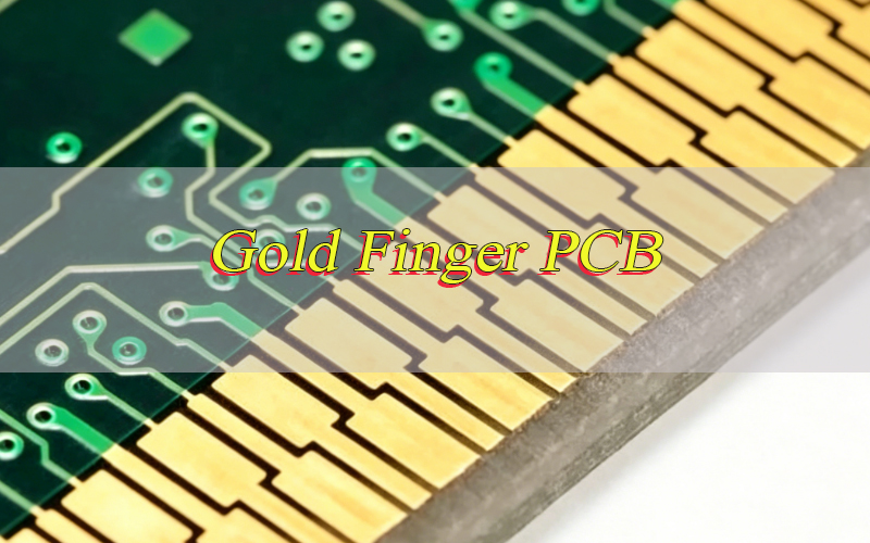
Which factors most directly impact the performance, durability, and signal stability of gold finger PCB, and how can design and manufacturing missteps that lead to product failure be avoided? This guide breaks down standard bevel angles, plating processes, thickness selection, design principles, and manufacturer identification to provide practical, actionable insights for gold finger PCB that meets application demands and maintains long-term reliability.
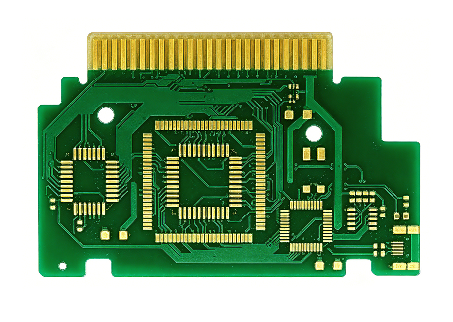
What Is the Standard PCB Gold Finger Bevel Angle and How to Design It Properly?
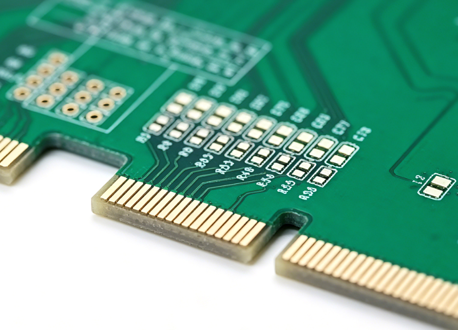
PCB gold finger typically uses a standard bevel angle between 30 and 45 degrees, with 45 degrees being the most widely adopted for most use cases. This range balances mechanical protection, smooth insertion, and effective contact area to prevent damage to the gold plating during insertion while ensuring consistent electrical connectivity. Stepping outside this range often leads to performance issues.
- Standard Angle Ranges and Application Scenarios: A 45-degree angle works best for vertical insertion setups such as memory modules and graphics cards, as it provides smooth guidance to minimize friction and scratching of the gold layer during insertion. A 30-degree angle is better suited for horizontal insertion applications like PCIe slots, as it reduces contact pressure and lessens wear on both the gold finger and its mating connector. Angles below 20 degrees create sharp edges that scratch mating contacts and cause uneven plating due to current concentration. Angles above 60 degrees reduce the effective contact area and drive up contact resistance.
- Design Considerations for Bevel Angles: Start by matching the angle to the insertion method. Vertical insertion calls for a steeper 45-degree angle for guidance, while horizontal insertion requires a shallower 30-degree angle to reduce pressure. Bevel depth should fall between 0.5mm and 1.0mm. Depths under 0.5mm fail to provide adequate guidance, and depths over 1.0mm weaken the PCB’s edge structure. Maintain a minimum 0.5mm gap between the bevel edge and the nearest circuit trace to prevent trace damage during bevel processing.
- Manufacturing Feasibility Checks: For electroless nickel gold plating processes, the bevel angle should not drop below 30 degrees. Electroless plating deposits more slowly on sharp edges, resulting in thin, inconsistent plating. Electroplating processes can handle angles as low as 20 degrees but require fixtures to control current distribution and avoid excessive edge plating. Clearly note the bevel angle, depth, and tolerance on design drawings. Angles should have a ±5-degree tolerance, and depth a ±0.15mm tolerance.
What Are the Steps in the PCB Gold Finger Plating Process?
The PCB gold finger plating process includes eight core steps. Strict control of each step’s parameters ensures uniform plating, strong adhesion, and corrosion resistance. The two most common processes, electroless nickel immersion gold (ENIG) and electrolytic gold plating, require slight adjustments to these steps based on the method used.
- Pre-Plating Surface Preparation: Clean the PCB surface to remove oil, oxides, and contaminants. Begin with an organic acid-based degreaser to eliminate oil and reduce surface tension for even solution coverage. Rinse thoroughly with deionized water after degreasing. Next, microetch the copper surface using a sodium persulfate solution to remove thin oxide layers and create a slightly rough surface that improves nickel layer adhesion. Keep copper ion concentration in the microetch solution between 3-20g/L to maintain a stable etching rate.
- Acid Pickling and Pre-Dipping: Use dilute sulfuric acid to remove oxides formed after microetching and any residual salts. Rinse with deionized water, then immerse the PCB in a pre-dip solution (AR grade sulfuric acid) to maintain the activation tank’s acidity and keep the copper surface fresh for effective activation in the next step.
- Activation Treatment: Immerse the PCB in a palladium activation solution to form a thin palladium layer on the copper surface via displacement reaction. This palladium layer acts as a catalyst for the subsequent electroless nickel plating. Keep activation temperature below 30℃, avoid aeration, and ensure the solution is free of chloride, iron, or nickel impurities to prevent activation failure.
- Electroless Nickel Plating: Deposit a nickel layer on the activated copper surface. This layer acts as a barrier between copper and gold to prevent mutual diffusion. Control plating temperature between 80-90℃ and pH between 4.5-5.5. The nickel layer should be 2-5μm thick for sufficient adhesion and corrosion resistance, with a uniform finish free of pinholes or bubbles.
- Gold Plating: For ENIG processes, immerse the PCB in an immersion gold solution to replace nickel with gold, forming a thin (0.1-0.3μm) yet highly conductive gold layer. For electrolytic gold plating, use an electrolytic solution with gold cyanide as the main component and apply a constant current to deposit a thicker (1-5μm) gold layer ideal for high-wear applications. Maintain gold purity above 99.9% for optimal electrical performance.
- Gold Recovery and Rinsing: Recover excess gold from the gold plating solution to reduce costs and environmental impact. Rinse the PCB thoroughly with deionized water multiple times to remove residual plating chemicals that can cause corrosion if left on the surface.
- Post-Plating Cleaning and Drying: Clean the PCB surface with a dilute sulfuric acid or citric acid solution to remove any remaining impurities, then dry it in a high-temperature oven (80-100℃) to prevent moisture-induced oxidation of the gold layer.
- Quality Inspection: Use a thickness gauge to verify nickel and gold layer thickness. Check for plating defects like unevenness, copper exposure, bubbles, or scratches. Conduct adhesion tests (tape tests) to ensure the plating layer does not peel when tape is applied and removed.
How to Choose the Right PCB Gold Finger Plating Thickness for Different Projects?
Selecting the correct PCB gold finger plating thickness depends on three core factors: insertion frequency, application environment, and electrical performance requirements. Thicker gold layers boost wear resistance but increase costs, while thinner layers reduce costs but may not meet durability needs. Aligning thickness with project requirements ensures optimal performance and cost-effectiveness.
- Consumer Electronics Applications: For devices with low insertion frequency (fewer than 1,000 cycles) such as USB dongles, mobile phone chargers, and tablet connectors, a thin gold layer (0.1-0.3μm) using ENIG is sufficient. This thickness balances cost and basic corrosion resistance. For devices with moderate insertion frequency (1,000-5,000 cycles) like memory modules and external hard drives, a 0.5-1.0μm gold layer ensures durability.
- Industrial Control Applications: Industrial equipment including PLC controllers, sensors, and server motherboards requires high durability (5,000-10,000 insertion cycles) and resistance to harsh environments. A 1.0-3.0μm gold layer using electrolytic gold plating is ideal. The nickel layer should be 3-5μm thick to enhance corrosion resistance in high-humidity and dusty settings.
- Aerospace and Military Applications: These applications demand extreme durability (10,000+ insertion cycles) and resistance to extreme temperatures, vibration, and corrosion. A 3.0-5.0μm gold layer with high purity (99.99%) is required. The nickel layer should be 5-8μm thick, and additional corrosion protection such as conformal coating may be necessary.
- High-Speed Signal Applications: For high-speed devices like 5G base stations and PCIe 5.0 interfaces, a thin (0.1-0.2μm) high-purity gold layer is preferred. Thicker gold layers can increase signal loss and impedance mismatch. ENIG ensures a smooth surface that reduces signal reflection and insertion loss.
- Key Considerations: Gold layer thickness is not a case of “thicker is better.” Thickness exceeding 5μm can create internal stress in the gold layer, leading to cracking or peeling. Match gold thickness to nickel layer thickness; the nickel layer should be 3-5 times the gold layer thickness to ensure strong adhesion. Electrolytic gold plating is more expensive than ENIG, so use it only when high wear resistance is necessary.
What Are the Critical Design Principles for High-Quality Gold Finger PCB?
Designing high-quality gold finger PCB requires balancing electrical performance, mechanical durability, and manufacturing feasibility. Following these critical principles avoids common design flaws such as poor contact, plating peeling, and signal interference to ensure the product meets application requirements.
- Bevel and Edge Design: Stick to the standard 30-45 degree bevel angle range and 0.5-1.0mm depth. Round the gold finger’s corners to avoid sharp edges that scratch mating connectors and damage the plating. Ensure the gold finger extends 2mm beyond the mating connector’s contact area to guarantee full contact.
- Solder Mask Design: Do not apply solder mask to the gold finger area. Keep the solder mask fully open to prevent ink peeling during insertion, which can cause contact failure. The solder mask opening should be 4mil larger than the gold finger line on each side, and no solder mask openings should be placed within 2mm of the gold finger.
- Circuit Trace Design: Keep gold finger lead widths between 12-40mil, with main leads at 40mil and secondary leads at 20mil. Use rounded corners for leads to avoid right-angle bends that cause signal reflection. Maintain a minimum 6mil spacing between adjacent gold fingers to prevent short circuits and crosstalk.
- Plating Layer Matching: Use a nickel barrier layer between the copper substrate and gold layer to prevent copper-gold diffusion, which degrades electrical performance. The nickel layer thickness should be 2-8μm depending on the application, and the gold layer thickness should align with insertion frequency and environment.
- PCB Thickness and Material Selection: PCB thickness should be 0.8-2.4mm, matching the mating connector’s slot thickness. Use high-quality FR-4 substrate for general applications and polyimide substrate for high-temperature or flexible applications. Ensure the substrate has good dimensional stability to prevent warpage that can disrupt gold finger alignment.
- Test Point Design: Add test points near the gold finger to facilitate electrical testing of contact resistance and signal integrity. Place test points 1-2mm away from the gold finger to avoid interfering with plating and insertion.
How to Ensure Signal Integrity in Gold Finger PCB Design for High-Speed Applications?
High-speed applications including 5G, PCIe 5.0, and high-frequency radar require gold finger PCB to maintain signal integrity by minimizing signal reflection, insertion loss, and crosstalk. Control impedance matching, reduce signal attenuation, and optimize layout design to achieve this.
- Impedance Matching Design: The gold finger and its connected transmission lines should have consistent impedance, typically 50Ω or 75Ω depending on the application. Calculate the gold finger width (for example, 0.8mm for 50Ω impedance on FR-4 substrate) and length (no more than 8mm) to avoid impedance sudden changes. Use a microstrip line extension structure with a 1mm gradual transition to create a smooth connection between the gold finger and transmission line, reducing return loss.
- Minimize Insertion Loss: Use high-purity gold (99.99%) for the gold layer to reduce conductor loss. Keep the gold layer thin (0.1-0.2μm) to avoid excessive signal absorption. Polish the gold finger surface to ensure a smooth finish (Ra ≤ 0.10μm) that reduces signal loss caused by surface roughness.
- Reduce Crosstalk: Maintain a minimum 1mm spacing between adjacent gold fingers. Arrange high-speed signal gold fingers alternately with ground fingers to form a shielding structure that reduces electromagnetic interference. Use equal-length design for gold finger leads, with a length difference of no more than 0.1mm to avoid signal time delay.
- Shielding and Grounding: Add a ground plane below the gold finger area to provide a reference ground and reduce signal radiation. Connect the ground plane to the gold finger’s ground leads with multiple vias to improve grounding effectiveness. Avoid placing high-speed signal traces near the gold finger edge to prevent signal leakage.
- Material Selection: For high-speed applications, use low-loss substrate materials like FR-4 with a low dielectric constant (εr ≤ 4.5) and low loss tangent (tanδ ≤ 0.02). For ultra-high-speed signals (above 32Gbps), use advanced materials like PTFE to further reduce signal loss.
What Quality Standards Should Gold Finger PCB Meet for Industrial and Aerospace Use?
Gold finger PCB used in industrial and aerospace applications must meet strict quality standards to ensure reliability in harsh environments including extreme temperatures, vibration, humidity, and corrosion. These standards cover plating quality, mechanical performance, electrical performance, and environmental resistance.
- Plating Quality Standards: Comply with IPC-4552, the industry standard for gold plating on PCB. Gold layer purity must be ≥99.9% for industrial use and ≥99.99% for aerospace use. Nickel layer thickness should be 3-8μm, and gold layer thickness 1.0-5.0μm depending on the application. Plating must be uniform, with no copper exposure, bubbles, scratches, or peeling. The tape test should show no plating detachment.
- Mechanical Performance Standards: For industrial use, gold finger must withstand 5,000+ insertion cycles without significant wear or increased contact resistance. For aerospace use, this number rises to 10,000+ cycles. The PCB should have a flexural strength of ≥150MPa and no warpage exceeding 0.75mm per 100mm length. Bevel angles must meet a ±5-degree tolerance, and edge roughness should be Ra ≤ 0.10μm.
- Electrical Performance Standards: Contact resistance must be ≤50mΩ and remain stable after 1,000 insertion cycles. Insulation resistance must be ≥10^10Ω at 500V DC. Dielectric strength should be ≥1kV/mm to prevent breakdown. For high-speed applications, insertion loss must be ≤0.3dB and crosstalk ≤-35dB.
- Environmental Resistance Standards: Gold finger PCB must pass a 72-hour salt spray test (5% NaCl concentration) with no corrosion or plating peeling. It should withstand high-temperature testing (-55℃ to 125℃ for industrial use, -65℃ to 150℃ for aerospace use) without performance degradation. It must also pass a humidity test (85% relative humidity at 85℃ for 1000 hours) with no insulation failure.
- Certification Requirements: Industrial gold finger PCB must meet ISO9001 and RoHS certification. Aerospace gold finger PCB must comply with AS9100 certification and meet MIL-STD-202 standards for environmental testing. All products must have full traceability of materials and manufacturing processes.
What Are the Common Challenges in Gold Finger PCB Manufacturing and How to Solve Them?
Gold finger PCB manufacturing involves complex processes. Common challenges include uneven plating, poor adhesion, plating peeling, copper exposure, and impedance mismatch. These issues can be resolved through strict process control, careful material selection, and thorough quality inspection.
- Uneven Plating: This issue stems from uneven current distribution, impure plating solution, or inadequate surface preparation. Use fixtures to ensure uniform current distribution during electroplating. Regularly filter the plating solution to remove impurities. Strengthen pre-plating cleaning to ensure the copper surface is free of oil and oxides. Keep plating temperature and pH within the recommended range.
- Poor Plating Adhesion: Insufficient microetching, contaminated activation solution, or improper nickel plating parameters cause poor adhesion. Extend microetching time slightly to create a rougher copper surface. Replace the activation solution regularly to avoid impurity contamination. Control nickel plating temperature and pH to ensure proper nickel layer formation. Conduct adhesion tests after plating to catch issues early.
- Plating Peeling: Excessive internal stress in the gold layer, insufficient nickel layer thickness, or poor substrate quality lead to plating peeling. Limit gold layer thickness to less than 5μm to reduce internal stress. Ensure the nickel layer is 3-5 times the gold layer thickness. Use high-quality substrates with strong adhesion to the nickel layer. Avoid rapid temperature changes during drying that can build up stress.
- Copper Exposure on Gold Finger: Incomplete solder mask opening, uneven plating, or scratches during handling cause copper exposure. Improve solder mask opening accuracy to ensure full coverage of the gold finger area. Increase plating time slightly to ensure complete coverage. Use anti-scratch packaging during handling and manufacturing. Carefully inspect the gold finger surface after plating.
- Impedance Mismatch: Incorrect gold finger width, length, or substrate material leads to impedance mismatch. Calculate impedance accurately based on substrate parameters and adjust gold finger dimensions accordingly. Use low-loss substrate materials for high-speed applications. Test impedance after manufacturing and adjust the design if needed.
How to Identify a Reliable China Gold Finger PCB Manufacturer?
Choosing a reliable China gold finger PCB manufacturer is critical to ensuring product quality, on-time delivery, and responsive technical support. Evaluate certification, production capacity, quality control, technical capabilities, and customer service to make the right choice.
- Certification and Compliance: The manufacturer should hold ISO9001 certification for quality management and RoHS certification for environmental compliance. For aerospace or military applications, verify AS9100 and MIL-STD-202 certifications. Ensure the manufacturer adheres to IPC standards for gold finger PCB manufacturing.
- Production Capacity and Equipment: Confirm the manufacturer has advanced production equipment, including automatic vertical electroplating lines, thickness gauges, impedance testers, and AOI inspection equipment. Check that production capacity aligns with your order volume and delivery timeline. Automated production lines ensure consistent quality and reduce human error.
- Quality Control System: A reliable manufacturer has a strict quality control system covering raw material inspection, in-process testing, and final inspection. Raw materials such as substrate and plating chemicals must undergo quality testing. In-process testing includes checks for plating thickness, adhesion, and impedance. Final inspection covers visual inspection, electrical testing, and environmental testing. Request quality control reports for previous orders.
- Technical Capabilities: The manufacturer should have professional technical teams capable of providing design support, DFM analysis, and custom solutions. They should handle complex designs such as high-speed gold finger PCB and aerospace-grade products. Ask about their experience in your specific industry and request case studies or samples.
- Customer Service and Delivery: Reliable manufacturers offer timely technical support and communication. They should respond to inquiries within 24 hours and provide clear order updates. Check their delivery record to ensure on-time delivery (a delivery rate of ≥98% is ideal). Ask about their after-sales service policy, including return and replacement options for defective products.
- Pricing and Cost Transparency: The manufacturer should provide transparent pricing with no hidden fees. Compare quotes from multiple manufacturers, but avoid choosing the lowest price if it compromises quality. A reliable manufacturer will share a detailed cost breakdown and explain price differences based on materials and processes.
FAQs About Gold Finger PCB
Q1: Can damaged gold finger PCB be repaired, and what are the effective repair methods?
A1: Damaged gold finger PCB can be repaired based on damage severity: Minor oxidation: Clean with anhydrous alcohol/specialized cleaner and polish with an eraser. Moderate scratches/thin plating: Touch up with a professional gold plating pen (match original gold layer thickness). Severe copper exposure/deep scratches: Re-plate (strip old plating, reprocess surface, re-plate nickel and gold). Application note: Non-critical applications only; replace PCB for aerospace/high-reliability industrial use.
Q2: What factors should be considered when selecting a PCB gold finger connector?
A2: Select PCB gold finger connectors by matching these key factors: Connector slot thickness matches PCB thickness (0.8-2.4mm); gold finger extends 2mm beyond connector contact area; contact force 10-30g per pin; high-speed applications: low contact resistance (≤50mΩ) and low crosstalk; harsh environments: corrosion-resistant materials (stainless steel/nickel plating).
Q3: How to prevent gold finger PCB from oxidation during storage and use?
A3: Prevent gold finger oxidation with these measures: Store in sealed packaging with desiccants (relative humidity ≤60%); avoid direct hand contact (use gloves); harsh environments: apply conformal coating to non-contact areas; regular maintenance: clean with anhydrous alcohol to remove dust/contaminants.
Q4: What is the difference between hard gold and soft gold plating for gold finger PCB?
A4: Soft gold (99.99% pure): high conductivity/ductility, suitable for low-insertion-frequency applications. Hard gold (gold + 5-10% cobalt/nickel): higher hardness/wear resistance, ideal for high-insertion-frequency use. Selection principle: Choose based on insertion frequency and performance needs.
Q5: How to test the quality of gold finger PCB after manufacturing?
A5: Gold finger PCB quality testing methods: Use a thickness gauge to verify nickel/gold layer thickness; conduct tape test forplating adhesion; measure contact resistance (≤50mΩ) with a multimeter; test impedance for high-speed applications; conduct environmental tests (salt spray/high-temperature) for industrial/aerospace use; visually inspect for defects under a magnifying glass.