Is your PCB Bluetooth antenna giving the product stable 2.4GHz wireless performance after assembly? In Bluetooth and BLE devices, antenna layout affects connection range, signal strength, power efficiency, and pairing consistency in real use.
A PCB bluetooth antenna works together with the RF feed line, ground plane, matching circuit, enclosure, battery, and nearby metal parts. This guide explains how to choose antenna types, arrange the PCB layout, design trace antennas, reduce common mistakes, and test the board before production.
What is a PCB Bluetooth Antenna?
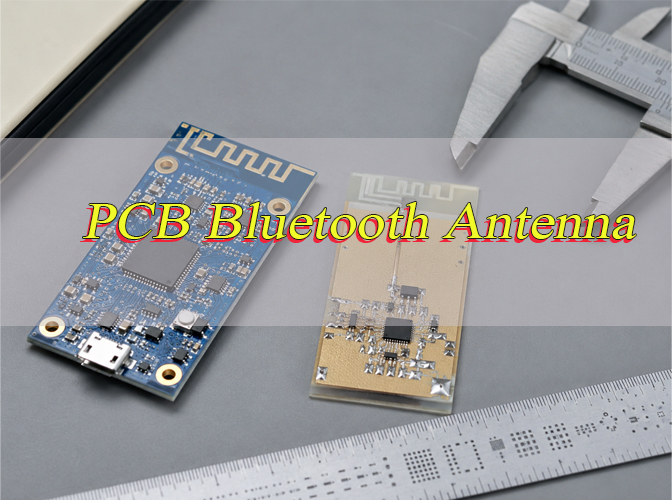
A PCB Bluetooth antenna is a wireless antenna formed on or mounted to a printed circuit board for Bluetooth or BLE communication. It usually works in the 2.4GHz ISM band and sends or receives radio-frequency energy through a designed radiating structure.
The antenna may be a copper trace, a compact chip antenna, or a module-based antenna area. Its performance depends on antenna shape, PCB layout, ground plane, surrounding components, and final product enclosure.
For small wireless products, the antenna is often one of the most sensitive areas of the layout. A small change near the antenna area can shift frequency response, reduce range, or make tuning more difficult.
How Does a Bluetooth PCB Antenna Work?
A Bluetooth PCB antenna works by converting high-frequency electrical signals into electromagnetic waves, then receiving those waves from nearby devices. In a real board, the antenna does not work alone. It is part of a complete RF path.
- Bluetooth IC or module: Generates and receives the 2.4GHz RF signal.
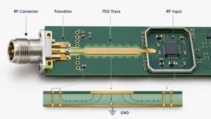
- RF feed line: Carries the signal from the chip or module to the antenna. It is normally designed as a 50-ohm controlled line.
- Matching network: Uses small capacitors or inductors to tune impedance between the RF source and the antenna.
- Antenna radiator: The copper trace or chip antenna structure that radiates energy into free space.
- Ground plane: Acts as the antenna’s reference area and strongly affects efficiency.
- Product enclosure: Plastic, metal, glass, battery position, cable routing, and hand placement can change final antenna behavior.
A stable antenna design balances these elements instead of treating the antenna as a separate copper shape.
What Are the Main Types of Bluetooth Antenna on PCB?
Bluetooth antenna on PCB designs can use several structures. The right choice depends on board size, cost target, available space, enclosure shape, and required wireless range.
- PCB trace antenna: This is a copper pattern directly etched on the PCB. It has low material cost and works well when enough board space and clearance are available.
- Inverted-F antenna, IFA: This common 2.4GHz antenna structure has a feed point and ground connection. It can offer a practical balance of size and performance.
- Meandered inverted-F antenna, MIFA: This pattern folds the antenna trace to save space. It is widely used in compact Bluetooth and BLE devices.
- Chip antenna: This is a small ceramic or multilayer component placed on the PCB. It saves board area, but still requires the correct ground area and matching design.
- Module antenna area: Some Bluetooth modules include a built-in antenna. The host PCB must still follow the module maker’s keepout and placement rules.
- External antenna connector: For longer range or challenging enclosures, a connector and external antenna may be used.
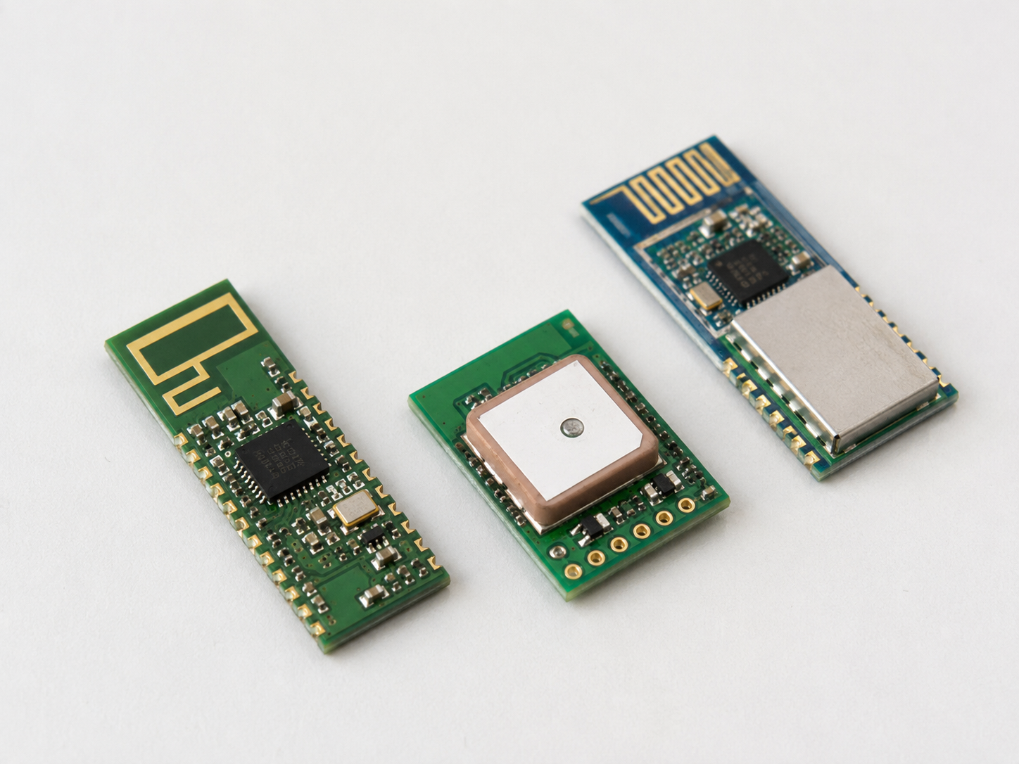
For many IoT, sensor, handheld, and wearable products, PCB trace antenna and chip antenna solutions are the two most common paths.
Bluetooth Chip Antenna vs PCB Antenna: Which Is Better?
Both antenna styles can work well when they are designed correctly. The better choice depends on product size, available layout area, cost plan, and tuning goals. A PCB antenna usually saves component cost, while a chip antenna can reduce occupied area.
| Comparison Item | PCB Trace Antenna | Bluetooth Chip Antenna |
|---|---|---|
| Board Space | Requires a defined edge area and clear keepout zone | Uses less physical antenna area |
| BOM Cost | Lower because the antenna is part of the copper pattern | Higher because it adds a discrete antenna part |
| Layout Sensitivity | Very sensitive to ground, copper, and nearby parts | Also sensitive, but vendor layout guidance helps |
| Tuning | Matching network is strongly recommended | Matching network is usually required |
| Range Potential | Good when layout and ground plane are well designed | Good in compact layouts when placed correctly |
| Manufacturing Control | Depends on trace accuracy, stackup, copper, and solder mask | Depends on placement accuracy and antenna part consistency |
| Best Fit | Cost-focused BLE devices, tags, sensors, and modules with enough space | Wearables, small handheld devices, dense IoT boards, and space-limited designs |
A practical selection starts with available board area. If the product has enough edge clearance, a trace antenna can be efficient and economical. If space is tight, a chip antenna may be easier to fit, but it still requires careful placement and final tuning.
What Are the Best Practices for Bluetooth Antenna PCB Layout?
Good Bluetooth antenna PCB layout starts before the board is routed. The antenna area, ground clearance, feed line, and nearby components should be planned during the first placement stage.
- Place the antenna near the PCB edge. Edge placement helps the antenna radiate away from the board and product body.
- Reserve a clean keepout zone. Keep copper, traces, vias, screws, shields, displays, batteries, and cables away from the antenna area.
- Use a 50-ohm RF feed line. Confirm trace width, dielectric thickness, and reference ground with the PCB stackup.
- Keep the feed line short and direct. Long or curved RF routes can add loss and mismatch.
- Place matching parts close to the antenna feed. Leave pads for a pi-network or similar tuning structure.
- Avoid routing under the antenna. Signal traces and copper pours below the radiator can disturb performance.
- Control ground stitching near the RF path. Use vias to keep the RF return path stable, while keeping the antenna keepout clear.
- Check enclosure and battery position early. A large battery, metal cover, or nearby cable can detune the antenna after assembly.
- Follow the antenna maker’s reference layout. For chip antennas and modules, the reference board layout is often the safest starting point.
- Build tuning samples before volume production. Real boards should be measured and adjusted before the design is locked.
How to Design PCB Bluetooth Antenna for Stable Wireless Performance?
A reliable antenna design starts before routing begins. The antenna shape matters, but it is only one part of the full RF path. Feed line impedance, ground plane, matching parts, PCB stackup, enclosure space, and nearby metal all influence final Bluetooth performance. For bluetooth pcb trace antenna design, the goal is to create a repeatable 2.4GHz structure that still performs well after assembly.
Step 1: Check the Available Space First
Start with the real product size, not only the PCB outline. Check where the battery, housing, display, screws, cables, and metal parts will sit. If the board has enough open edge space, a PCB trace antenna can work well. If the product is very compact, a chip antenna or Bluetooth module antenna may be easier to place.
Step 2: Choose the Right Antenna Type
Select the antenna based on board size, cost target, range requirement, and layout freedom. A trace antenna saves BOM cost and suits many BLE products. A chip antenna takes less board area but still requires correct clearance and tuning. A module antenna can simplify RF design, but the host PCB must follow the module layout guide.
Step 3: Place the Antenna at the Board Edge
The antenna should usually be placed at the PCB edge or corner. This helps it radiate away from the board and reduces interference from dense circuitry. Avoid placing it near batteries, metal shields, USB ports, large connectors, displays, or mounting screws.
Step 4: Reserve a Clear Keepout Area
The antenna zone should stay free from copper pour, signal traces, vias, test pads, and components. This rule should apply to related layers, not just the top layer. A clean keepout area gives the antenna more stable radiation space and reduces frequency shift after assembly.
Step 5: Route a Controlled 50-Ohm RF Feed Line
The RF feed line connects the Bluetooth chip or module to the antenna. It should be designed as a 50-ohm transmission line according to the PCB stackup. Keep it short, direct, and smooth. Avoid sharp corners, unnecessary vias, long detours, or routing through noisy circuit areas.
Step 6: Add a Matching Network
Leave a footprint for a matching circuit, usually a pi-network made with capacitors and inductors. This small area is very useful during tuning. Even if the first layout follows a reference design, the final housing, battery, and nearby components may still shift antenna performance.
Step 7: Control the Ground Plane Carefully
The ground plane is part of the antenna system. Keep a solid reference ground under the RF feed line, but do not pour copper into the antenna keepout zone. Ground stitching vias can be placed near the RF path to improve return current control, while the radiator area should remain clear.
Step 8: Follow the Reference Pattern Closely
For a PCB trace antenna, start from a proven 2.4GHz reference pattern. Do not casually shorten, stretch, rotate, or reshape the antenna trace. Small geometry changes can alter resonance. For chip antennas, follow the antenna supplier’s land pattern, clearance area, feed layout, and ground rules.
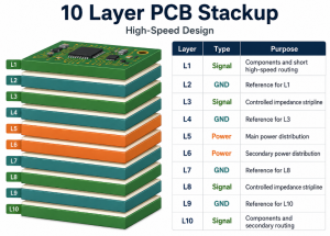
Step 9: Confirm PCB Stackup and Material Details
PCB thickness, dielectric constant, copper thickness, solder mask, and fabrication tolerance all affect antenna behavior. Keep the stackup consistent from prototype to production. If the reference antenna is designed with solder mask coverage, the manufactured board should follow the same condition.
Step 10: Test with the Complete Product
A board may perform well in open air but change after final assembly. Test the antenna with the housing, battery, display, cables, and mechanical parts installed. Measure return loss, impedance, range, and connection stability. Adjust the matching parts when required, then lock the final layout, stackup, and matching values for production.
What Does a Bluetooth Antenna on PCB Pattern Look Like?
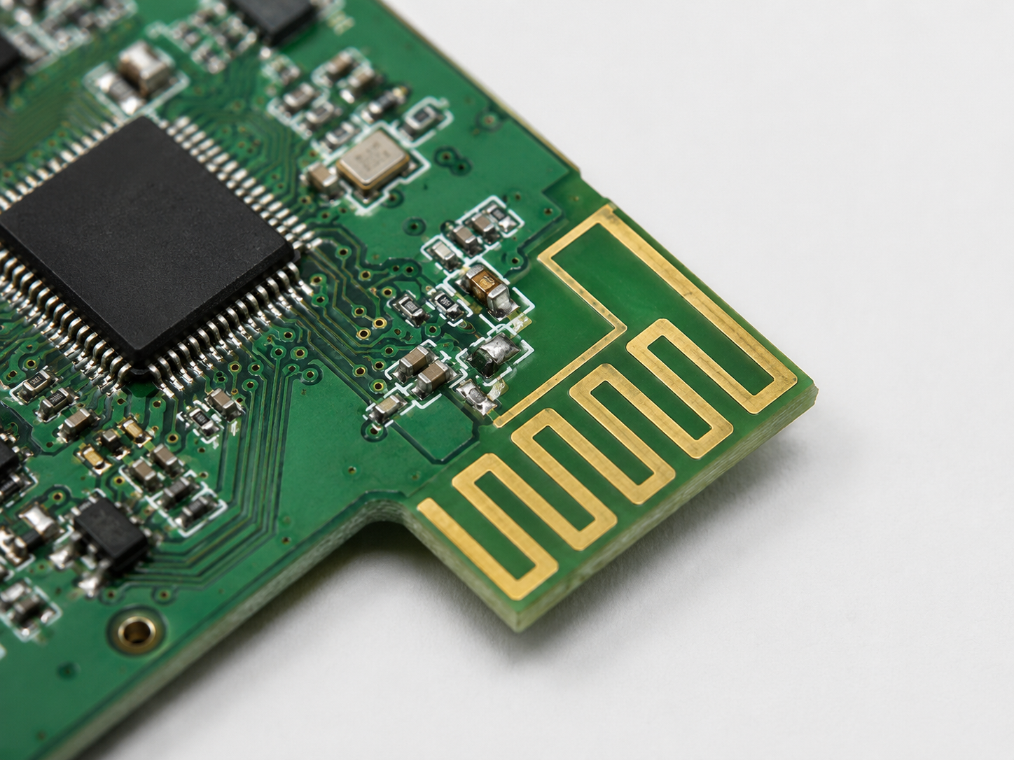
A Bluetooth antenna on PCB pattern is usually placed at the edge or corner of the board. It may look like a straight copper strip, an L-shaped trace, an inverted-F structure, or a folded meander line.
A simple monopole pattern can be used when there is enough length and clearance. In compact boards, a meandered pattern is common because it folds the radiating path into a smaller area while still targeting the 2.4GHz band.
The visible shape is only part of the design. The ground plane beside the pattern, feed location, shorting point, keepout area, and dielectric environment all affect final behavior.
For chip antenna designs, the pattern may look simpler because the antenna body is a mounted component. However, the land pattern, ground clearance, feed trace, and matching network remain critical to performance.
In practical layout work, the antenna pattern should not be treated as decorative copper. It is an RF structure that must match the board, device size, and final product environment.
How Does PCB Material Affect Bluetooth Antenna Performance?
PCB material affects Bluetooth antenna performance through dielectric constant, thickness, loss, copper profile, and tolerance. At 2.4GHz, these factors can shift impedance and change antenna resonance.
Standard FR4 is widely used for many Bluetooth and BLE products. For compact or more performance-sensitive designs, tighter stackup control and stable material data can make tuning easier.
Solder mask also changes the environment around a copper trace antenna. Some reference antennas specify whether the antenna trace is covered or exposed, so the manufactured board should follow the approved design closely.
Material choice alone does not create a strong antenna. Stable fabrication, controlled trace geometry, consistent board thickness, and proper assembly are just as important.
What Mistakes Should You Avoid in Bluetooth PCB Antenna Design?
Many Bluetooth antenna problems come from layout shortcuts rather than from the antenna type itself. Early planning helps prevent weak signal, short range, unstable connection, and late tuning changes.
- Placing metal too close to the antenna: Batteries, shields, screws, connectors, and cables can absorb or disturb RF energy.
- Ignoring the keepout area: Copper pours, vias, and traces in the antenna zone can change resonance.
- Using a random antenna pattern: A copied pattern may fail if the board size, material, or ground plane is different.
- Skipping the matching network: Without tuning parts, it becomes harder to correct mismatch after prototype testing.
- Routing the RF feed like a normal signal trace: The RF line should be treated as a controlled transmission line.
- Changing stackup after antenna design: Thickness or dielectric changes can affect impedance and tuning.
- Testing only the bare board: The final enclosure, battery, display, cable, and nearby hand position can change performance.
- Placing the antenna deep inside the PCB outline: Center placement usually limits radiation and increases coupling with other circuits.
- Starting production before RF validation: Prototype measurement gives useful data before large batch manufacturing.
How to Test and Tune a PCB Bluetooth Antenna?
Testing and tuning help confirm whether the antenna works as expected in the real device. A design that looks correct in layout software still requires physical measurement, because RF behavior changes with assembly and enclosure details.
Step 1: Check the PCB layout before fabrication
Review antenna position, feed width, ground clearance, keepout, stackup, and matching pads. This step helps catch visible layout issues before boards are made.
Step 2: Measure impedance and return loss
Use a vector network analyzer to check the antenna around the 2.4GHz band. S11 and return loss data show how much RF energy is reflected back instead of radiated.
Step 3: Adjust the matching network
Change capacitor or inductor values in the matching circuit to bring the antenna closer to the desired impedance range. This is where reserved matching pads provide real design flexibility.
Step 4: Test with the full enclosure
Measure again after adding housing, battery, display, and mechanical parts. This gives a more realistic view of final performance.
Step 5: Run wireless range checks
Test connection stability at different distances, orientations, and product positions. BLE devices may also require checks under low-power operating modes.
Step 6: Prepare the production build record
Once tuning is complete, lock the antenna area, matching values, material stackup, and assembly notes for consistent manufacturing.
Where Is a PCB Bluetooth Antenna Commonly Used?
Bluetooth antennas on PCB are widely used in compact wireless products that require short-range communication, low power use, and convenient connection with phones, gateways, sensors, or control units.
- IoT sensors: Temperature sensors, humidity sensors, asset trackers, and smart meters.
- Wearable devices: Fitness bands, healthcare monitoring devices, and portable electronics.
- Medical electronics: Handheld instruments, monitoring modules, and connected diagnostic devices.
- Industrial control devices: Wireless control boards, data collection modules, and machine-side sensor nodes.
- Smart home products: Locks, switches, thermostats, lighting controllers, and appliance modules.
- Consumer electronics: Audio accessories, remote controls, game peripherals, and personal devices.
- Automotive accessories: Bluetooth control modules, diagnostic dongles, and in-cabin wireless devices.
- Lighting systems: BLE lighting controls, dimmers, sensor nodes, and smart LED modules.
How to Choose a Reliable PCB Bluetooth Antenna Manufacturer?
A reliable manufacturer should understand that a Bluetooth antenna area is part of the RF system, not just another copper feature. The fabrication process must support stable dimensions, clean etching, controlled stackup, and careful review before production.
- DFM review for antenna areas: The supplier should check spacing, copper clearance, solder mask, edge clearance, and possible manufacturing risks.
- Controlled impedance support: RF feed lines should be reviewed according to the confirmed stackup.
- Stable PCB material and thickness control: Consistent dielectric thickness helps keep RF behavior more repeatable.
- Accurate etching capability: Antenna traces and feed lines require clean geometry.
- Prototype and small-batch support: Early samples help verify layout and tune matching values before larger orders.
- PCBA assembly capability: Antenna tuning parts, RF chips, modules, and small passive components require controlled assembly.
- Testing coordination: The manufacturer should support electrical testing and work smoothly with RF validation plans.
- Traceability and quality records: Lot control, material records, and inspection data help maintain consistency across batches.
- Experience with wireless products: Prior work with BLE, IoT, RF modules, sensors, and compact electronics is valuable.
FAQs About PCB Bluetooth Antenna
Q1: Can Bluetooth use a PCB trace antenna instead of an external antenna?
A1: Yes. A PCB trace antenna can support Bluetooth and BLE communication when the layout is designed for the 2.4GHz ISM band. It is often used in sensors, smart home products, handheld devices, and compact wireless modules because it saves component cost and does not require an external antenna connector.
Q2: What frequency should a Bluetooth antenna on PCB support?
A2: A Bluetooth antenna on PCB should work around 2.4GHz to 2.4835GHz. This is the standard Bluetooth operating band. The antenna pattern, feed line, ground plane, and matching network should all be designed around this frequency range.
Q3: Is a chip antenna always better than a PCB antenna?
A3: Not always. A chip antenna is useful when board space is limited, but it still needs proper clearance, ground design, and tuning. A PCB trace antenna can be a better choice when the board has enough edge space and the project needs lower BOM cost. Both antenna styles usually need a 50-ohm RF feed line and a matching circuit.
Q4: How much clearance should be kept around a Bluetooth PCB antenna?
A4: Clearance depends on the antenna type and reference design. As a practical rule, the antenna area should be free from copper, vias, batteries, cables, shields, screws, and large metal parts. Many 2.4GHz antenna layouts require several millimeters of keepout, and some designs may require 5mm to 15mm or more depending on the structure.
Q5: Why does Bluetooth signal become weaker after the product is assembled?
A5: The antenna environment changes after assembly. Plastic housing, battery position, display modules, metal clips, charging cables, and hand contact can shift antenna tuning. That is why testing should be done with the complete product, not only the bare PCB. A design that works in open air may perform differently after final assembly.
Q6: Does PCB material affect Bluetooth antenna performance?
A6: Yes. PCB thickness, dielectric constant, copper thickness, solder mask, and manufacturing tolerance can affect antenna resonance and impedance. Standard FR4 is widely used for Bluetooth products, but stable stackup control is important. At 2.4GHz, even small changes in dielectric thickness or copper geometry can influence tuning.
Q7: Should the Bluetooth antenna trace be covered with solder mask?
A7: It depends on the reference design. Some antenna patterns are designed with solder mask coverage, while others require exposed copper. If the prototype antenna is tuned with solder mask coverage, the production PCB should keep the same condition to avoid frequency shift.
Q8: Why is a matching network required for a PCB antenna?
A8: A matching network helps tune the impedance between the RF circuit and the antenna. It usually uses small capacitors and inductors, often arranged as a pi-network. This allows the antenna to be adjusted after real-board testing. For Bluetooth designs, the RF path is commonly designed around 50 ohms.
Q9: Can the Bluetooth antenna be placed anywhere on the PCB?
A9: No. The antenna is usually placed at the PCB edge or corner to improve radiation. Placing it near the center of the board, close to a battery, under a display, or beside metal shielding can reduce wireless range. A clean edge location gives the antenna a better chance to radiate outward.
Q10: What should be checked before producing a Bluetooth antenna PCB?
A10: Before fabrication, check the antenna pattern, keepout area, RF feed width, ground plane, matching pads, PCB stackup, solder mask condition, and enclosure distance. For better production consistency, the final tuned design should lock the stackup, antenna geometry, and matching component values before batch manufacturing.
Conclusion
A PCB Bluetooth antenna can deliver stable wireless performance when the RF path, antenna area, ground reference, material stackup, and tuning process are planned together. The best results usually come from early layout discipline, controlled prototype builds, and real-device testing before production.
If you are preparing a Bluetooth, BLE, IoT, sensor, medical, industrial control, lighting, or compact wireless PCB project, EBest Circuit can support PCB fabrication(including FR4 PCB, RF circuit boards and so on), DFM review, controlled impedance guidance, PCBA assembly, component sourcing, and production-quality support. Send your Gerber files, stackup requirements, BOM, and product specifications to sales@bestpcbs.com for a quotation and technical review.