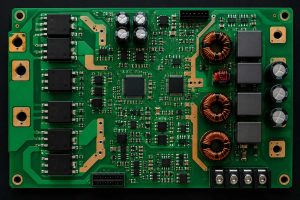
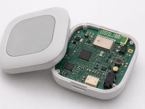
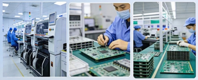
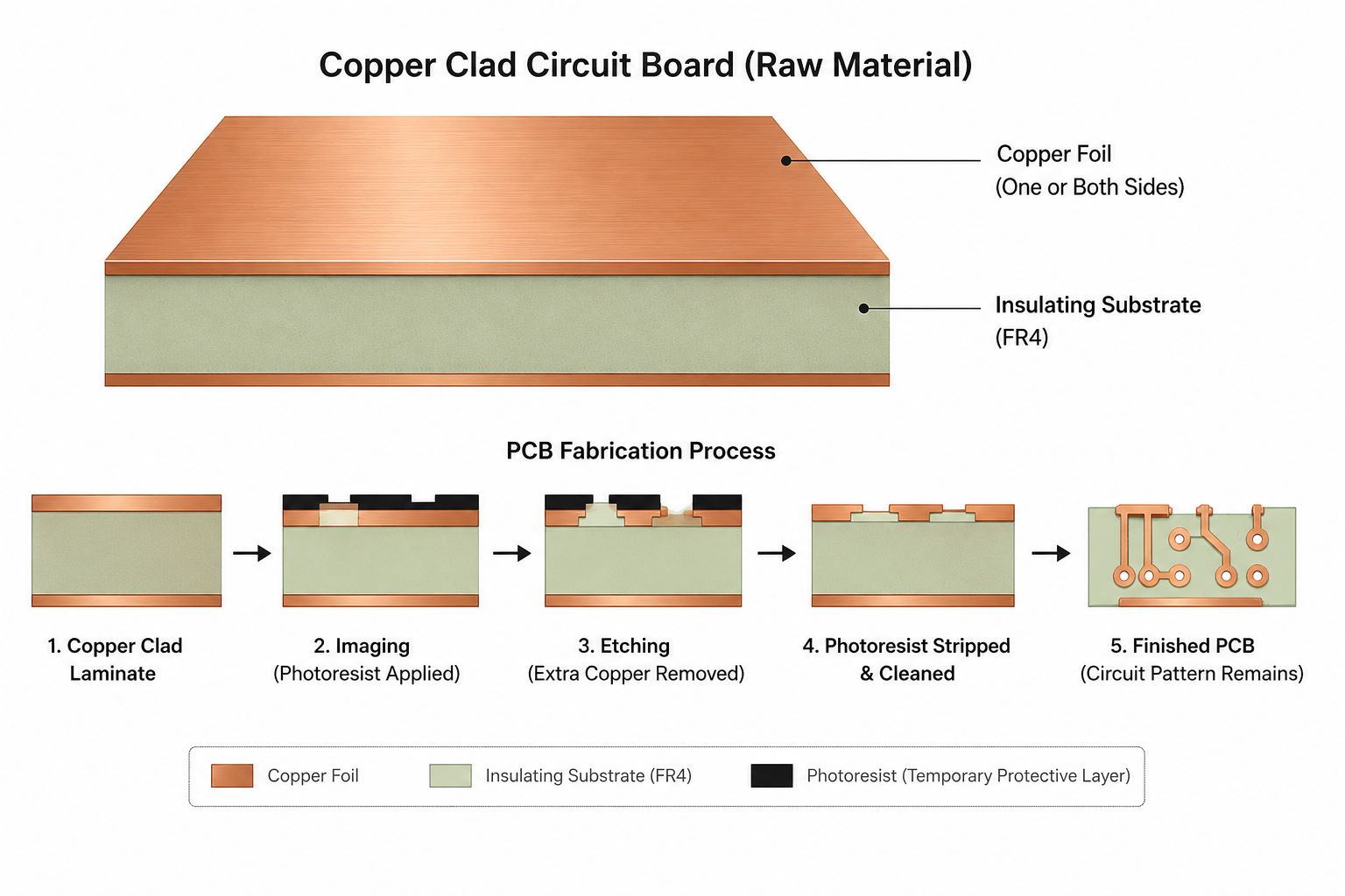
A copper clad circuit board is the base material used to make many printed circuit boards. It has an insulating board with copper foil on one or both sides. During PCB fabrication, the extra copper is removed. As a result, the needed circuit pattern is left on the board.
This guide explains the basic meaning, common materials, board types, and supplier selection points. In addition, it shows how EBest can support customers from PCB fabrication to PCBA assembly.
EBest provides custom copper clad PCB fabrication and PCBA assembly for prototypes, medium-volume, and high-volume production orders. Our team can review your material choice, copper thickness, board structure, surface finish, and assembly needs before production, helping you reduce design risk and move faster from bare PCB to finished PCBA. For material review or a quotation, send your Gerber files, BOM, drawings, or project requirements to sales@bestpcbs.com.
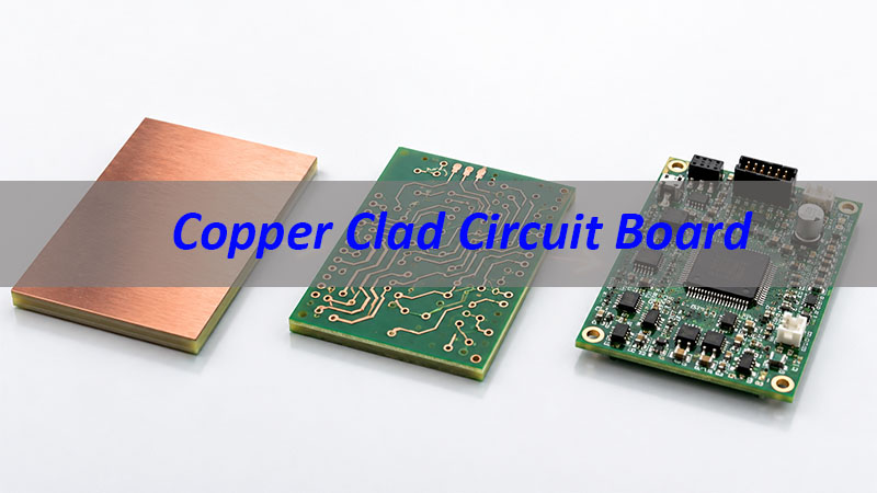
What Is a Copper Clad Circuit Board?
A copper clad circuit board is made by bonding copper foil to an insulating base material. The base material can be FR4, paper based material, CEM material, polyimide, metal base material, or another special laminate.
The copper layer is used to form the circuit. The base material supports the board and provides insulation. Therefore, both copper and substrate quality matter.
A simple copper clad board usually includes two main parts:
| Part | Function |
|---|---|
| Copper Foil | Forms traces, pads, and circuit patterns |
| Base Material | Provides support, insulation, heat resistance, and board strength |
In PCB production, the board goes through several steps. For example, it may need drilling, imaging, etching, plating, solder mask, surface finish, and inspection. After these processes, the copper clad material becomes a finished printed circuit board.
What Is a Copper Clad Printed Circuit Board Used For?
A copper clad printed circuit board is used in many electronic products. It provides the base for electrical connection and component mounting. Also, it helps carry signals or current between components.
Common applications include:
- Consumer electronics
- Industrial control boards
- LED lighting products
- Communication devices
- Automotive electronics
- Power supply modules
- Medical electronics
- Test instruments
- IoT devices
For simple products, a single sided board may be enough. However, more complex products often need double sided or multilayer PCB structures. This is because they need more routing space and better layout flexibility.
Therefore, the best board type depends on the circuit design. It also depends on current load, signal speed, working temperature, product size, and cost target.
Copper Clad Laminate Circuit Boards: What Material Options Are Available?
Copper clad laminate circuit boards can be made with different materials. Each material has its own purpose. So, buyers should not choose only by price or appearance.
Here are some common material options:
| Material Type | Common Use |
|---|---|
| Paper Based CCL | Simple and low cost electronics |
| FR4 Glass Fiber CCL | General PCB manufacturing |
| CEM Material CCL | Cost sensitive products with better strength than paper material |
| High Tg FR4 CCL | Boards that need better heat resistance |
| Low Loss CCL | High speed or high frequency circuits |
| Metal Based CCL | LED, power, and heat dissipation applications |
| Flexible CCL | Flexible PCB and compact electronic products |
Among these options, FR4 is one of the most common choices. It offers good strength, insulation, process stability, and cost balance. Because of this, it is widely used in standard PCB production.
However, some projects need special materials. For example, LED boards may need better heat transfer. High speed boards may need lower signal loss. In these cases, material selection should be reviewed before production.
What Copper Clad Circuit Board Material Should You Choose?
The right copper clad circuit board material should match the product’s real working conditions. Before choosing the material, engineers should first check heat, current, signal speed, soldering temperature, board thickness, and final use environment.
A simple selection logic is:
| Design Need | Suggested Material Direction | Key Reason |
|---|---|---|
| General control circuit | Standard FR4 copper clad board | Balanced cost, strength, and insulation |
| Lead free soldering or higher heat | High Tg FR4 | Better thermal stability |
| LED or power product | Metal core PCB or copper core PCB | Better heat transfer |
| High current circuit | Heavy copper PCB | Better current carrying capacity |
| High speed or RF signal | Low loss laminate | Lower signal loss and stable impedance |
| Compact multilayer design | Stable FR4 or special laminate | Better layer alignment and process control |
For heat sensitive products, material selection should not rely on guesswork.
Engineers can use a simple thermal estimate:
ΔT = P × Rθ
- In this formula, ΔT is temperature rise, P is power loss, and Rθ is thermal resistance. If power loss is high, the board needs a better thermal path.
Thermal resistance can also be estimated by:
Rθ = t / (k × A)
- Here, t is dielectric thickness, k is thermal conductivity, and A is heat transfer area. So, a thinner dielectric layer, higher thermal conductivity, or larger heat spreading area can help reduce temperature rise.
- This is why standard FR4 is suitable for many control boards, but it may not be the best choice for LED lighting, automotive lighting, power modules, or high current products. In those cases, metal core PCB, copper core PCB, or heavy copper PCB may be more suitable.
- For high speed or RF designs, the key points are different. Engineers should focus on Dk, Df, impedance control, copper roughness, stackup thickness, and material stability. These factors can affect signal loss and transmission quality.
At EBest, we review copper clad circuit board material together with the actual PCB design. Our engineering team can check copper thickness, board thickness, Tg value, thermal path, dielectric layer, surface finish, and assembly process before production. This helps customers choose a material that fits both performance and manufacturing needs.
Instead of only producing boards according to files, EBest can provide DFM review, material suggestions, PCB fabrication, component sourcing, PCBA assembly, and testing. This is especially useful when customers are not sure whether to use FR4, high Tg FR4, metal core PCB, copper core PCB, heavy copper PCB, or low loss laminate.
FR4 Copper Clad Circuit Board: When Is It the Right Choice?
An FR4 copper clad circuit board is suitable for many standard PCB projects. FR4 is made from glass fiber cloth and epoxy resin. It offers good strength and electrical insulation.
FR4 is commonly used in:
- Industrial control PCB
- Consumer electronics PCB
- Communication device PCB
- Power supply PCB
- Automotive auxiliary electronics
- Instrument control boards
- General multilayer PCB designs
FR4 is a good choice when the project needs stable quality and reasonable cost. Also, it has mature manufacturing support. Therefore, it is often the first option for many PCB designs.
However, not all FR4 materials are the same. Standard FR4, high Tg FR4, halogen free FR4, and low loss FR4 have different properties. So, the material grade should be confirmed before production.
This is especially important for boards with high temperature, dense components, controlled impedance, or strict reliability needs.
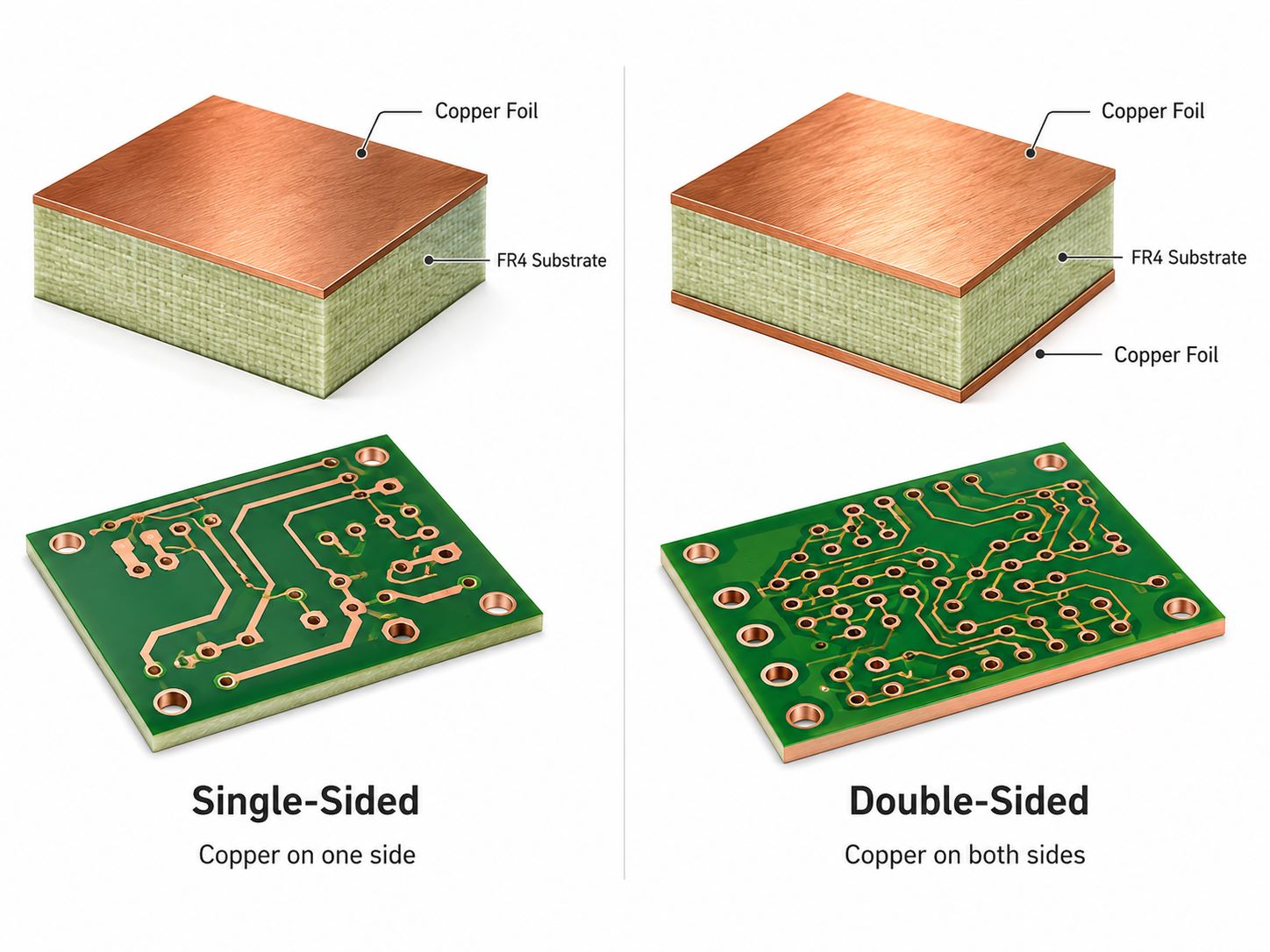
Single Sided Copper Clad Circuit Board vs Double Sided Copper Clad Circuit Board
Single sided and double sided boards are two common choices. The difference is simple. However, it can strongly affect layout, cost, and production.
| Type | Structure | Best For |
|---|---|---|
| Single Sided Copper Clad Circuit Board | Copper on one side only | Simple circuits, low cost products, LED boards, basic control boards |
| Double Sided Copper Clad Circuit Board | Copper on both sides | Denser layouts, more routing space, plated holes, compact products |
A single sided copper clad circuit board is easier to make. Also, it usually costs less. It works well when the circuit is simple and all routing can be done on one side.
A double sided copper clad circuit board gives more design space. It allows traces on both sides of the board. In addition, plated through holes can connect the two copper layers. As a result, the layout can be smaller and cleaner.
Therefore, the choice depends on layout density, current needs, assembly method, board size, and target cost.
Copper Clad Circuit Board vs Copper Core PCB: What Is the Difference?
A copper clad circuit board and a copper core PCB both use copper. However, they are not the same product.
A copper clad circuit board usually means an insulating laminate with copper foil on the surface. The copper is etched to form circuit traces.
A copper core PCB has a copper core or copper base inside the board structure. The copper core is mainly used for heat spreading. Therefore, it is often used in high power and high heat products.
| Item | Copper Clad Circuit Board | Copper Core PCB |
|---|---|---|
| Main Purpose | Form circuit traces | Improve heat dissipation |
| Copper Position | Copper foil on laminate surface | Copper core or copper base |
| Common Use | General PCB fabrication | High power LED, automotive lighting, power modules |
| Design Focus | Circuit routing and insulation | Thermal path and heat transfer |
| Cost Level | Usually more flexible | Usually higher due to special structure |
If your product needs normal signal routing, a standard copper clad PCB may be enough. However, if heat is the main concern, copper core PCB or metal core PCB may be a better choice.
How to Choose a Copper Clad Circuit Board Manufacturer or Supplier?
Choosing a manufacturer is not only about price. The supplier should understand PCB materials, copper thickness, board tolerance, surface finish, and assembly needs.
Before ordering, buyers should check these points:
- Can the supplier support the required material?
- Can they make single sided, double sided, and multilayer PCBs?
- Can they control copper thickness and line spacing?
- Can they provide DFM review before production?
- Can they support prototypes and mass production?
- Can they also provide PCB assembly?
- Can they source components if needed?
- Do they have testing and quality control?
DFM review is very useful. It means Design for Manufacturing review. In this step, engineers check whether the board can be produced smoothly.
For example, they may check trace spacing, hole size, copper weight, solder mask clearance, and board stackup. As a result, many hidden risks can be found before production.
A good supplier should help you avoid production issues early. Also, they should support both quality and delivery control.
What Copper Clad Circuit Board Services Does EBest Provide?
EBest provides custom copper clad circuit board manufacturing support. In addition, we can support the full process from PCB fabrication to PCBA assembly.
Our services include:
- Custom PCB fabrication
- FR4 PCB manufacturing
- Single sided PCB production
- Double sided PCB production
- Multilayer PCB fabrication
- Metal core PCB support
- Copper core PCB support
- High Tg PCB manufacturing
- DFM pre review
- BOM optimization
- Component sourcing
- SMT assembly
- Through hole assembly
- Functional testing
- Quality inspection
- Prototype and small batch production
For copper clad PCB projects, EBest can review the material, copper thickness, board structure, surface finish, and assembly needs before production. Therefore, customers can reduce material mismatch and process risks.
Also, EBest can support different industries. These include industrial control, medical electronics, automotive electronics, communication products, LED lighting, and other electronic devices. Our factory operates under certified quality systems, including ISO 9001, ISO 13485, IATF 16949, and AS9100D. Our products are also manufactured in compliance with UL, REACH, and RoHS requirements.
If you need bare PCB fabrication, assembled PCBA, or turnkey electronics manufacturing, EBest can help from prototype to production.
FAQs About Copper Clad Circuit Board
Q1: What is a copper clad circuit board?
A1: A copper clad circuit board is an insulating board with copper foil on one or both sides. During PCB fabrication, the copper is etched to form the circuit pattern.
Q2: Is copper clad laminate the same as PCB?
A2: Not exactly. Copper clad laminate is the base material. After drilling, etching, plating, solder mask, surface finish, and testing, it becomes a finished PCB.
Q3: What is the most common copper clad circuit board material?
A3: FR4 is one of the most common materials. It offers good insulation, board strength, heat resistance, and cost balance.
Q4: What is the difference between single sided and double sided copper clad boards?
A4: A single sided board has copper on one side. A double sided board has copper on both sides. Therefore, a double sided board offers more routing space.
Q5: Can copper clad circuit boards be used for high power products?
A5: Yes, but the material must be selected carefully. For better heat transfer, metal core PCB or copper core PCB may be more suitable.
Q6: Where can I get copper clad boards for printed circuit boards?
A6: You can source them from a PCB manufacturer that supports material selection, PCB fabrication, copper thickness control, surface finish, and assembly service.
Q7: Can EBest provide both copper clad PCB fabrication and assembly?
A7: Yes. EBest can support PCB fabrication, component sourcing, SMT assembly, through hole assembly, testing, and quality control.
In a nutshell, a copper clad circuit board is the foundation of many PCB products. It affects circuit quality, heat resistance, assembly results, and product reliability.
For standard projects, FR4 is often a practical choice. However, high heat, high speed, or special products may need other materials. Therefore, material review is important before production.
Need help with your copper clad PCB project? Send your Gerber files, BOM, drawings, or project requirements to sales@bestpcbs.com. EBest can support material review, PCB fabrication, component sourcing, PCBA assembly, testing, and production follow up.