Choosing a silkscreen circuit board manufacturer is not only about printing white text on a green PCB. For engineers, buyers, and project managers, PCB silkscreen affects component identification, assembly efficiency, polarity recognition, inspection, testing, field maintenance, and brand presentation.
A clear silkscreen layer helps operators locate parts faster. It helps technicians read polarity marks without hesitation. It also makes revision numbers, logos, test points, warning symbols, and manufacturing codes easier to recognize during production and after delivery.
In this guide, we will explain what a silkscreen circuit board is, how PCB silkscreen printing works, what design mistakes should be avoided, how to evaluate a manufacturer, and why EBest Circuit can support custom PCB projects that require clear marking and reliable fabrication. For project review or quotation support, you can also send your Gerber files, BOM, and requirements to sales@bestpcbs.com.
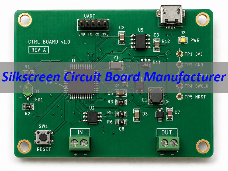
What Is a Silkscreen Circuit Board?
A silkscreen circuit board is a printed circuit board with a visible legend layer printed on the solder mask surface. This layer usually contains reference designators, component outlines, polarity symbols, pin-one marks, test point labels, warning icons, logos, part numbers, date codes, and revision information.
In PCB production, silkscreen is also called legend printing or nomenclature printing. Eurocircuits describes legend print, also known as silkscreen, as the process of applying text or patterns on top of the solder mask of a PCB. It is commonly used for component identification, polarity marks, serial numbers, repair functions, and logos.
For most boards, the silkscreen is printed on the component side. Some designs also use bottom-side silkscreen, especially when both sides contain components or when extra traceability information is needed. The color is usually white, but black, yellow, or other colors may be used depending on solder mask color and visual contrast.
A good silkscreen circuit board should be easy to read, properly aligned, resistant to normal handling, and free from markings printed over pads, vias, exposed copper, or component soldering areas.
Why Is Silkscreen Important in PCB Manufacturing?
Silkscreen looks simple, but it plays a practical role across the PCB manufacturing and assembly process.
It supports faster component placement.
- Clear reference designators such as R12, C8, U3, D1, and J5 help operators and inspectors quickly match the PCB with the BOM, placement file, and assembly drawing.
It reduces polarity confusion.
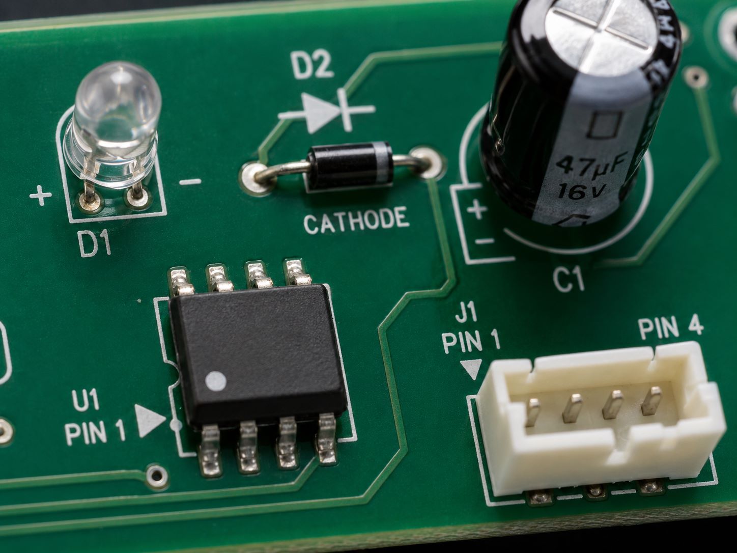
- Diodes, electrolytic capacitors, LEDs, connectors, ICs, and batteries often require clear orientation. A simple “+”, “-”, cathode mark, or pin-one dot can prevent assembly errors.
It improves testing and troubleshooting.
- Labels such as TP1, GND, 5V, RX, TX, SWDIO, and RESET make engineering debugging easier. During functional testing, technicians can identify test points without checking layout files repeatedly.
It helps with traceability.
- Revision numbers, batch codes, date codes, and customer part numbers help teams manage product versions. This is useful for industrial control, medical electronics, automotive electronics, communication equipment, and other regulated or long-lifecycle applications.
It improves brand presentation.
- A clean logo, product name, and board revision marking make the PCB look more professional, especially for demo units, evaluation boards, open-frame modules, and visible internal electronics.
Industry practice generally includes reference designators, polarity marks, pin-one indicators, component boundaries, logos, warning symbols, part numbers, revision numbers, and date codes as common PCB silkscreen markings.
How Does a Silkscreen Circuit Board Manufacturer Print PCB Markings?
A silkscreen circuit board manufacturer can use different printing methods depending on the project volume, board complexity, marking resolution, and production setup.
- Screen printing is the traditional method. Ink is pushed through a prepared mesh screen onto the PCB surface. It is efficient for batch production and works well for standard text, symbols, and component legends.
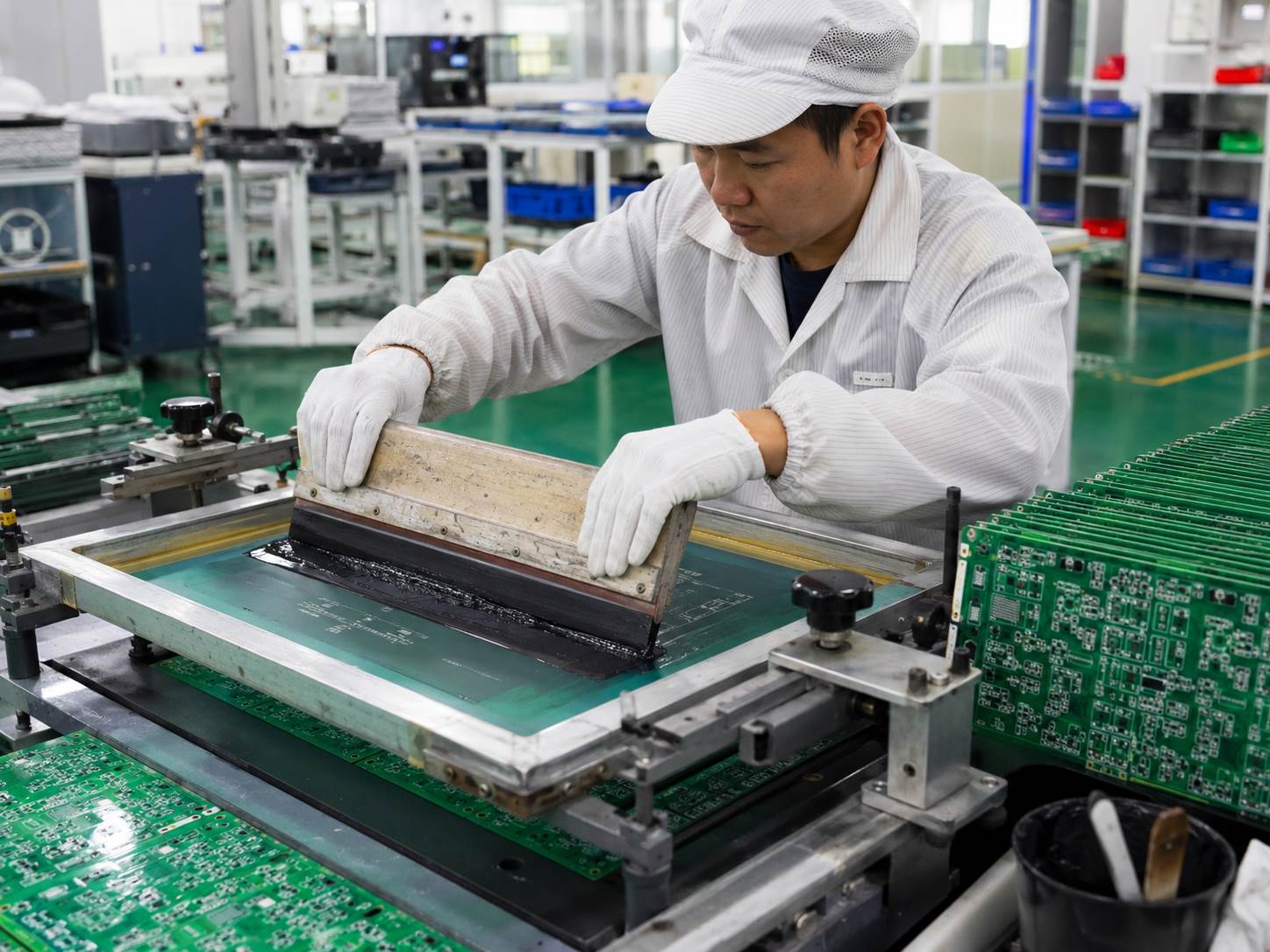
- Liquid photo imaging, also called LPI legend, can support finer marking than traditional screen printing. It is often used when the design has dense components or small character sizes.
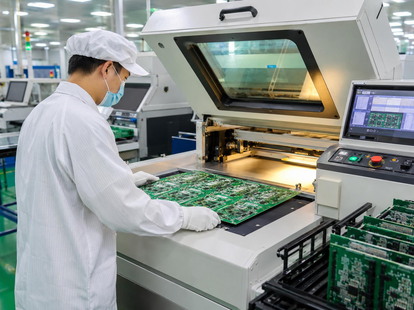
- Direct legend printing, also called inkjet printing, applies the legend digitally without a physical screen. This method can provide good flexibility for small batches, prototypes, serial numbers, QR-style markings, and variable data.
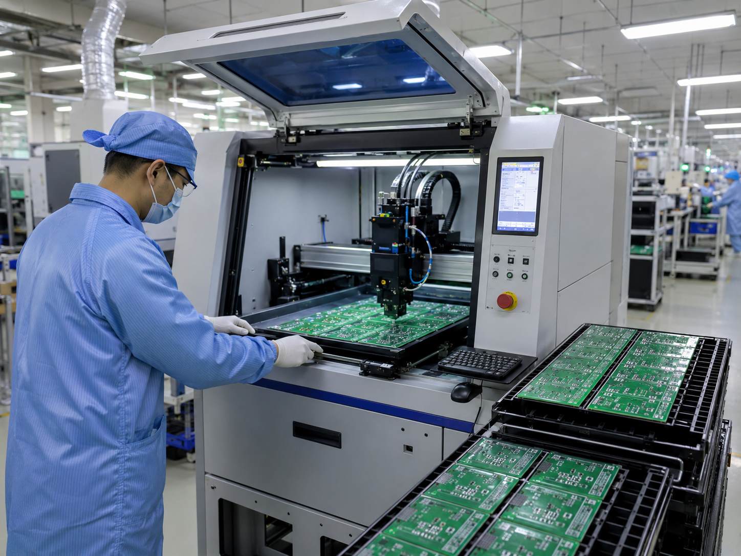
After printing, the ink is cured so that it adheres to the solder mask. The manufacturer then checks alignment, legibility, ink coverage, and whether any marking affects solderability.
For customers, the most important point is not only the printing method. The real value is whether the manufacturer can review the Gerber data before production and identify risks such as text over pads, labels too close to component outlines, unreadable fonts, or poor contrast between ink and solder mask.
What Information Should Be Included on a PCB Silkscreen Layer?
A useful PCB silkscreen layer should contain information that helps assembly, inspection, testing, identification, and maintenance.
Common silkscreen content includes:
- Reference designators: R1, C2, U5, L3, Q1
- Component outlines and placement boundaries
- Pin-one marks for ICs and connectors
- Polarity marks for LEDs, diodes, capacitors, and power terminals
- Test point labels such as TP1, GND, 3V3, 5V, SDA, SCL
- Connector names such as USB, UART, CAN, IN, OUT
- Switch positions such as ON/OFF, BOOT, RESET
- Warning symbols for high voltage, ESD-sensitive areas, or hot surfaces
- Product name, customer part number, board revision, and date code
- Company logo or approved brand mark
However, more silkscreen is not always better. A readable board uses enough information without crowding the layout. Dense silkscreen can become hard to read when components are small, spacing is tight, or solder mask contrast is limited.
For production-quality PCB design, silkscreen should be treated as an engineering layer, not a decorative afterthought.
What Materials and Inks Are Used for PCB Silkscreen Printing?
PCB silkscreen ink is commonly a non-conductive epoxy-based ink. JLCPCB notes that silkscreen ink is specially formulated to be non-conductive, with black and white being common industry colors. (JLCPCB)
The ink must bond well to the solder mask surface and remain readable after normal handling, assembly, reflow exposure, cleaning, and inspection. For many standard FR4 PCBs, white legend on green solder mask is the most common combination because it provides high contrast and easy readability.
Other common combinations include:
| Solder Mask Color | Common Silkscreen Color | Typical Use |
|---|---|---|
| Green | White | Standard PCB fabrication |
| Black | White or gray | Consumer electronics, premium-looking boards |
| White | Black | LED boards, lighting products, display modules |
| Blue | White | Prototypes, development boards |
| Red | White | Power modules, evaluation boards |
| Matte black | White or light gray | High-end electronics, visible internal boards |
Ink choice should match the solder mask color, application environment, readability requirement, and branding style. For LED, display, and optical products, the visual effect of solder mask and silkscreen may need extra review because reflection, glare, and contrast can affect product appearance.
How to Avoid Common Silkscreen PCB Design Mistakes?
Good silkscreen begins with good layout practice. Even a capable manufacturer may need to clip or remove markings if the Gerber file places legend ink over exposed copper, solder pads, or areas that affect assembly.
Keep silkscreen away from pads and exposed copper.
- Text printed over pads can affect soldering quality and may be automatically removed during CAM processing. Designers should leave enough clearance between legend features and solderable areas.
Use readable text size.
- Tiny fonts may look acceptable on a monitor but become blurred or unreadable after printing. For compact boards, use fewer words, shorter labels, and stronger placement logic.
Avoid placing text under components.
- Once the board is assembled, hidden labels cannot support inspection or maintenance. Key marks should remain visible after assembly whenever possible.
Use clear polarity symbols.
- For LEDs, diodes, electrolytic capacitors, connectors, and ICs, polarity marks should match the schematic and assembly drawing. Pin-one marks should be obvious and consistent.
Do not crowd the board edge.
- Silkscreen too close to routing edges, V-cuts, tabs, or tooling areas may become incomplete after panelization or separation.
Check contrast before production.
- White legend on green solder mask is easy to read. Black legend on dark solder mask may look refined but can reduce readability. For production boards, function should guide appearance.
Review the silkscreen layer together with solder mask and assembly files.
- A reliable silkscreen circuit board manufacturer should check Gerber files, solder mask openings, component placement, board outline, and silkscreen clearance together, not as isolated layers.
What Quality Standards Should a Silkscreen Circuit Board Manufacturer Follow?
Silkscreen quality should be controlled as part of the complete PCB manufacturing process. A clear legend layer is valuable, but it must not compromise solderability, electrical performance, dimensional accuracy, or assembly quality.
A reliable manufacturer should review:
| Quality Item | What Should Be Checked |
|---|---|
| Legibility | Text, symbols, reference designators, and markings should be readable |
| Alignment | Silkscreen should match component locations and board outline |
| Clearance | Legend ink should not cover pads, test points, exposed copper, or plated holes |
| Ink adhesion | Markings should remain stable after handling and standard process exposure |
| Contrast | Ink color should be readable against the solder mask color |
| Data consistency | Revision, logo, date code, and part number should match customer files |
| CAM review | Risky silkscreen features should be flagged before production |
| Final inspection | AOI, visual inspection, and electrical testing should be aligned with project needs |
For industrial, medical, automotive, aerospace, and communication products, documentation control is also important. The silkscreen layer often carries version and traceability information, so the manufacturer should treat it as part of the production record.
EBest Circuit can support PCB fabrication with DFM review, controlled manufacturing, electrical testing, AOI, X-ray inspection when required, PCBA assembly, component sourcing, and traceability support for prototype, small-batch, and production projects.
How to Choose a Reliable Silkscreen Circuit Board Manufacturer?
When selecting a silkscreen circuit board manufacturer, do not judge only by price. Clear marking is closely connected with fabrication control, CAM review, solder mask quality, assembly support, and communication efficiency.
Check whether the manufacturer reviews silkscreen during DFM.
- A good supplier should not simply print whatever appears in the Gerber file. They should identify unreadable text, silkscreen-pad overlap, poor clearance, missing polarity marks, and potential assembly confusion.
Confirm the manufacturer’s PCB capabilities.
- Silkscreen is usually part of a broader PCB requirement. Your project may also need controlled impedance, high TG FR4, MCPCB, heavy copper, rigid-flex, Rogers materials, ceramic substrates, ENIG, HASL, OSP, or other fabrication processes.
Ask about prototype-to-production support.
- Some suppliers are suitable for hobby prototypes. Others are stronger for engineering review, small-batch validation, and stable mass production. Choose based on your project stage.
Review assembly capability.
- If the board will move to PCBA, the manufacturer should understand BOM, placement files, polarity markings, test points, and component orientation. PCB silkscreen should support assembly, not conflict with it.
Evaluate quality and traceability.
- Look for inspection processes, material control, production documentation, batch traceability, and communication speed. For regulated applications, this matters more than a small unit price difference.
Check communication quality.
- Silkscreen problems are often small details: missing label, unclear revision, wrong logo orientation, or a polarity mark placed near the wrong pin. A responsive engineering team can prevent these details from turning into production delays.
Top 10 Silkscreen Circuit Board Manufacturers for PCB Projects
This list is a practical reference, not an official ranking. The best choice depends on your board type, location, lead time, quality requirements, cost target, and whether you need PCB fabrication only or full PCBA support.
| Manufacturer | Suitable Project Type | Practical Strength |
|---|---|---|
| EBest Circuit | Custom PCB, PCBA, industrial, medical, automotive, communication, lighting, RF, ceramic, MCPCB, rigid-flex projects | Engineering-driven PCB fabrication, DFM support, PCBA assembly, component sourcing, testing, and traceability support |
| AdvancedPCB | U.S.-based PCB projects, advanced PCB needs, IPC Class 2/Class 3 options | Offers PCB manufacturing capabilities from design through final assembly, covering small batch to high volume, HDI, RF/microwave, flex, rigid-flex, SMT, through-hole assembly, and layout services. |
| Sierra Circuits | Quick-turn PCB fabrication and turnkey projects | Provides PCB fabrication, assembly, and components, with quick-turn manufacturing and full turnkey board options. |
| JLCPCB | Online PCB prototypes, cost-sensitive projects, standard and advanced PCB orders | Offers online PCB prototype and fabrication services, Gerber viewer tools, PCB capabilities, assembly options, and listed silkscreen capability parameters. |
| PCBWay | Prototype PCB, EMS projects, PCB assembly, quick-turn work | Provides PCB prototype, fabrication, assembly, EMS-related services, and silkscreen resources for PCB marking. |
| Eurocircuits | European prototypes and small-series PCB projects | Focuses on PCB prototypes and small series in European facilities and publishes practical legend print design guidance. |
| Würth Elektronik CBT | European PCB projects, engineering consultation, technology standards | Offers PCB technology standards, manufacturing capability guidance, and consultation for suitable PCB solutions. |
| Sunstone Circuits | PCB manufacturing with defined capability review | Publishes detailed PCB manufacturing capabilities, including silkscreen-related capability information. |
| Bittele Electronics | Turnkey PCB assembly, prototype, low-to-mid volume projects | Positions itself as a turnkey PCB assembly company with prototype and low-to-mid volume PCB fabrication and assembly services. |
| San Francisco Circuits | Complex PCB production, prototype-to-production runs, advanced PCB technologies | Describes itself as a one-stop PCB shop handling complex PCB production from manufacturing to assembly for prototype and production runs. |
For buyers comparing suppliers, the key is not choosing the most famous name. The better approach is to choose the supplier whose process fits your product stage, quality level, documentation needs, and delivery schedule.
Case Study: How EBest Circuit Manufactured a Silkscreen Circuit Board for a Customer Project
A customer needed a 14-layer FR4 silkscreen circuit board for an industrial electronic control project. The board required clear marking, stable multilayer fabrication, thicker copper, and reliable solderability.
The PCB was designed with Tg170 FR4, 2 oz inner and outer copper, 2.4 mm ±10% board thickness, ENIG 2U” surface finish, green solder mask, white silkscreen, and tented vias.
EBest Circuit reviewed the Gerber files, stackup, copper thickness, solder mask, via treatment, and silkscreen layer before production. For this board, the main control points were multilayer lamination, copper thickness control, solder mask coverage, silkscreen alignment, and ENIG finish quality.
After fabrication, the finished PCB showed clean green solder mask, readable white silkscreen, well-covered tented vias, and stable multilayer quality. The clear silkscreen helped improve component identification, inspection, and preparation for PCBA assembly.
This case shows that a reliable silkscreen circuit board manufacturer should not only print clear markings, but also control the complete PCB fabrication process behind them.
PCB Parameters Used in This Case
| Item | Specification |
|---|---|
| PCB Type | Multilayer FR4 PCB |
| Layer Count | 14 Layers |
| Material | FR4, Tg170 |
| Copper Thickness | 2 oz inner / 2 oz outer |
| Board Thickness | 2.4 mm ±10% |
| Surface Finish | ENIG 2U” |
| Solder Mask | Green |
| Silkscreen | White |
| Via Treatment | Tented Vias |
| Application | Industrial electronic control project |
| Key Control Points | Lamination, copper thickness, solder mask, silkscreen alignment, ENIG finish |
Why Choose EBest Circuit as Your Silkscreen Circuit Board Manufacturer?
EBest Circuit supports customers who need more than simple PCB printing. We provide PCB fabrication, PCBA assembly, component sourcing, DFM support, testing, and production-quality communication from prototype to batch production.
Engineering review before production
- Our team can review Gerber files, solder mask openings, silkscreen clearance, board outline, drill files, stackup, copper spacing, via design, and manufacturability before production. This helps improve the final board before it reaches the factory floor.
Wide PCB manufacturing capability
- EBest Circuit can support FR4 PCB, high TG PCB, MCPCB, ceramic PCB, Rogers PCB, heavy copper PCB, rigid-flex PCB, extra-thin PCB, RF PCB, and other custom PCB requirements. For customers with different product lines, this gives more flexibility under one manufacturing partner.
PCB and PCBA one-stop support
- Silkscreen should support assembly. Because we provide both PCB fabrication and PCBA assembly, our team can review the board from a manufacturing and assembly perspective. This is especially useful for connector labels, polarity marks, test points, and revision control.
Quality control and testing support
- We can support electrical testing, AOI, X-ray inspection when needed, functional testing according to customer requirements, and production traceability. For products used in medical devices, industrial control, automotive electronics, communication equipment, lighting, UAV, and robotics, this process control helps customers move forward with confidence.
Prototype to production service
- Some projects start with a few prototype boards. Others require small-batch validation or mass production. EBest Circuit can support different stages, helping customers refine PCB design, confirm manufacturing details, and prepare for stable production.
If your project needs clear silkscreen marking, reliable PCB fabrication, and PCBA support, EBest Circuit can review your Gerber files, BOM, assembly drawings, and production requirements before quotation.
FAQs About Silkscreen Circuit Board Manufacturer
Q1: What does a silkscreen circuit board manufacturer do?
A1: A silkscreen circuit board manufacturer fabricates PCBs with printed legend markings such as component labels, polarity symbols, test point names, logos, revision codes, and warning marks. A capable manufacturer also reviews whether the silkscreen is readable, properly aligned, and clear of solder pads.
Q2: Is PCB silkscreen required on every circuit board?
A2: Not always. Some very small or highly cost-sensitive boards may use limited marking. However, most engineering, industrial, testing, and assembly-focused PCBs benefit from clear silkscreen because it improves identification, inspection, and maintenance.
Q3: What is the best color for PCB silkscreen?
A3: White silkscreen on green solder mask is the most common choice because it offers strong contrast and good readability. Black silkscreen is often used on white solder mask, especially for LED boards, display modules, and products where appearance matters.
Q4: Can silkscreen be printed on both sides of a PCB?
A4: Yes. Silkscreen can be printed on the top side, bottom side, or both sides. Double-sided silkscreen is useful when components, test points, or identification marks appear on both sides of the board.
Q5: Why does my manufacturer remove some silkscreen text from the PCB?
A5: Manufacturers may remove or clip silkscreen that overlaps pads, vias, exposed copper, or solderable areas. This protects solderability and avoids ink contamination on areas that need reliable electrical or mechanical connection.
Q6: What files are needed for PCB silkscreen printing?
A6: The manufacturer usually needs Gerber files that include top silkscreen and/or bottom silkscreen layers. For PCBA projects, assembly drawings, BOM, centroid files, and polarity information are also useful.
Q7: How small can PCB silkscreen text be?
A7: Minimum text size depends on the manufacturer’s process capability, ink method, solder mask color, and board density. For production boards, it is better to use readable text rather than pushing the minimum limit.
Q8: Can EBest Circuit manufacture silkscreen circuit boards with PCBA assembly?
A8: Yes. EBest Circuit can support PCB fabrication, silkscreen printing, component sourcing, PCBA assembly, inspection, testing, and traceability support. Customers can send Gerber files, BOM, and assembly requirements for engineering review and quotation.
In a nutshell, a good silkscreen circuit board is easy to read, useful during assembly, consistent with the BOM and layout, and durable enough for normal production handling. Clear marking helps engineers, operators, inspectors, and field technicians work with the board more efficiently.
Looking for a silkscreen circuit board manufacturer that can support both clear PCB marking and reliable fabrication? Pls feel free to send your Gerber files, BOM, stackup requirements, and project details to EBest Circuit at sales@bestpcbs.com. Our team can provide DFM review, PCB manufacturing, PCBA assembly, testing, and quotation support for your next custom PCB project.