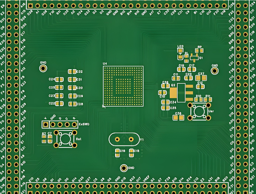
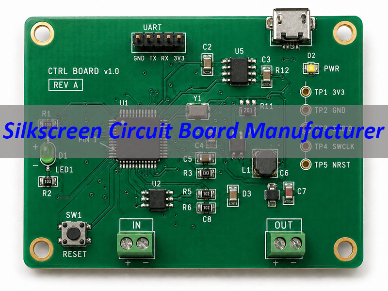
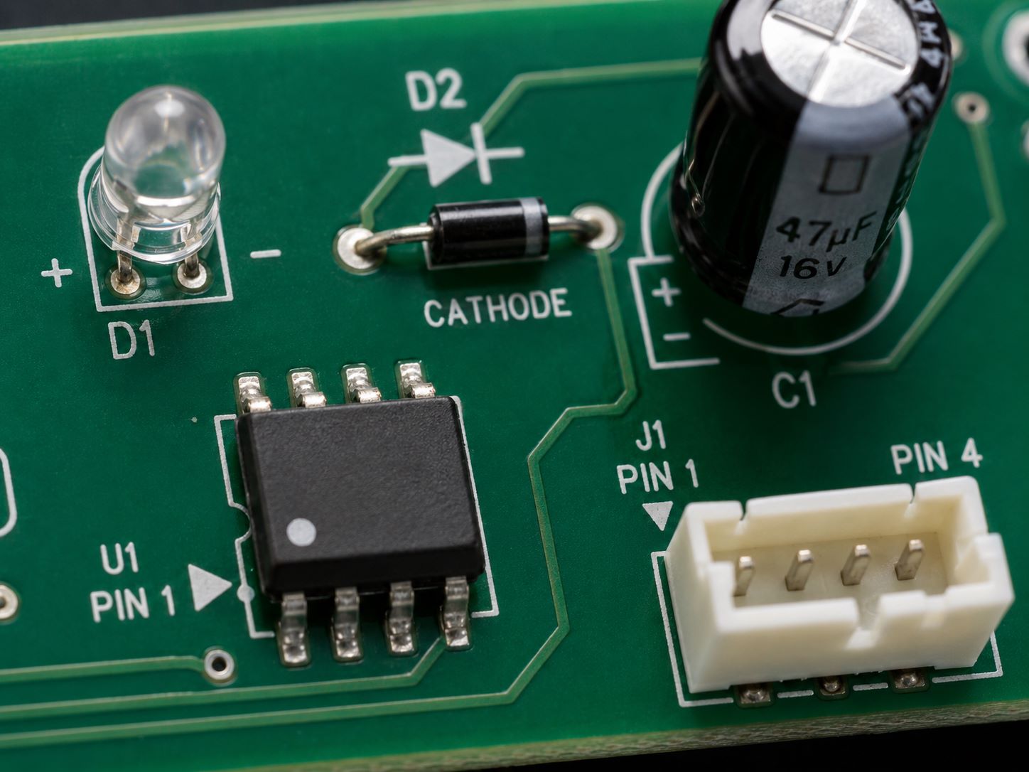
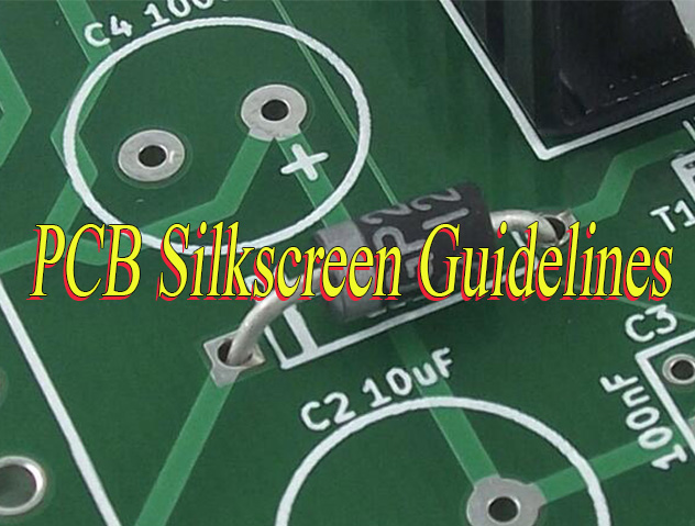
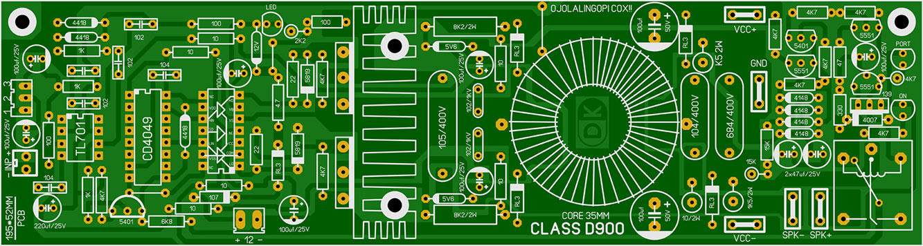
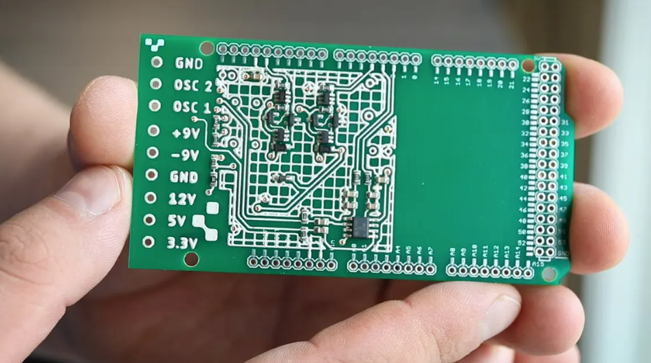
A PCB missing silk screen usually does not stop the bare circuit board from conducting electricity, but it can create real problems during assembly, inspection, testing, repair, traceability, and field maintenance. The silkscreen, also called the legend layer or overlay layer, carries human-readable information such as reference designators, polarity marks, pin-1 indicators, connector labels, warning symbols, part numbers, revision codes, date codes, and compliance marks.
When this information is missing, operators may need to rely only on drawings, pick-and-place data, BOM files, and test fixtures. This increases handling time and raises the risk of assembly mistakes, especially in high-mix, low-volume PCB assembly or custom OEM production.
What Is PCB Silkscreen?
PCB silkscreen is the printed marking layer on the top side, bottom side, or both sides of a printed circuit board. It is not a conductive copper layer. Its main role is to show readable information for engineers, assemblers, inspectors, test technicians, and repair teams.
Typical PCB silkscreen content includes component reference designators such as R12, C8, U3, Q1, and J2. It also includes pin-1 marks for ICs, BGAs, connectors, and modules, as well as polarity marks for diodes, LEDs, tantalum capacitors, and electrolytic capacitors.
Silkscreen can also show connector names, test point labels, switch positions, jumper instructions, board names, version numbers, date codes, lot codes, QR codes, logos, warning marks, and compliance symbols.
Why Is Silkscreen Important on a PCB?
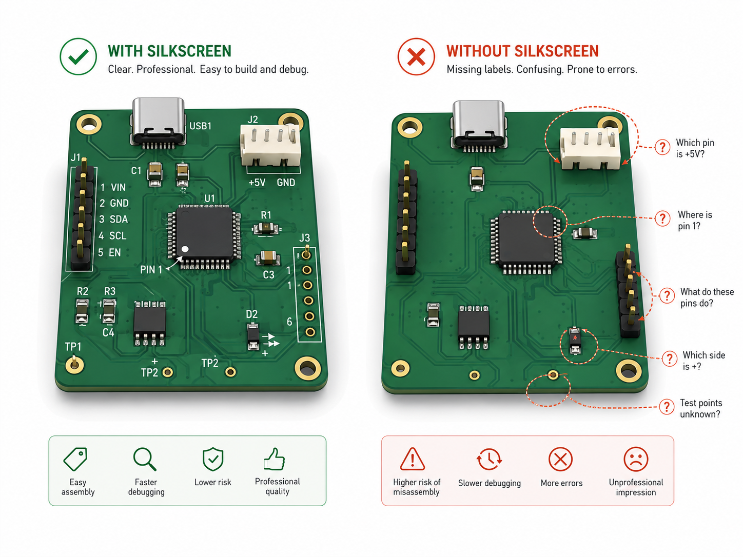
Silkscreen is important because it connects digital design data with real production handling. A PCB file may contain perfect information, but once the board reaches SMT, DIP assembly, inspection, testing, or field repair, technicians need fast visual confirmation.
A good silkscreen helps people answer simple but critical questions:
- Where is U1?
- Which side is pin 1?
- Which connector is power input?
- Which LED direction is correct?
- Which test point should be used for voltage measurement?
- Which board revision is this?
- Is this product compliant with the required marking plan?
PCB silkscreen is a low-cost layer that improves production clarity. In dense PCB layouts, not every marking can be printed, so the most important information should be prioritized.
What Happens When a PCB Is Missing Silk Screen?
When a PCB is missing silk screen, the electrical circuit may still work if the copper, solder mask, drilling, plating, surface finish, and assembly are all correct. The main risk is not usually immediate electrical failure. The main risk is human error.
A missing silkscreen can cause:
- Slower SMT line setup and first article inspection
- Higher chance of wrong component orientation
- More difficult manual soldering and rework
- More time spent checking assembly drawings
- Confusion during functional testing
- Harder field troubleshooting
- Weak traceability when part numbers, revision marks, date codes, or UL-related markings are required
- More communication between the customer, PCB manufacturer, and assembly factory
For prototypes, this may only delay engineering review. For batch production, especially OEM and ODM projects, the cost can be much higher because one small orientation mistake may affect hundreds or thousands of boards.

Does Missing Silkscreen Affect PCB Function?
In most cases, missing silkscreen does not directly affect electrical performance. The silkscreen ink does not carry current, define impedance, create insulation between copper layers, or control solder joint formation when it is correctly kept away from pads.
However, it can indirectly affect product function if it leads to assembly mistakes. For example, if a diode polarity mark is missing and the assembly team installs the diode in the wrong direction, the circuit may fail. If a connector pinout is missing, cable installation may become confusing. If test point labels are absent, technicians may probe the wrong point during debugging.
How Does PCB Silkscreen Work in Manufacturing?
PCB silkscreen is generated from the top overlay and bottom overlay layers in PCB design software. During CAM engineering, the PCB manufacturer checks whether the silkscreen overlaps exposed copper pads, solder mask openings, vias, fiducials, or other features where ink should not be printed.
Silkscreen can be applied by several methods:
| Method | Common Use | Main Benefit | Main Limitation |
|---|---|---|---|
| Screen printing | Standard PCB production | Cost-effective for volume | Less suitable for very fine text |
| Liquid photo imaging | Higher precision legend work | Better definition | Higher process requirement |
| Direct legend printing | Digital printing and flexible data marking | Good for variable data, QR codes, and serial numbers | Equipment and process control matter |
| Inkjet printing | Modern production, short runs, custom data | Fast changeover | Ink adhesion and readability must be verified |
The printing method influences the minimum text height, line width, clearance, registration tolerance, and final readability. This is why a design that looks clear in CAD may become unreadable or partially deleted after CAM cleanup if it violates factory capability.
Main Types of PCB Silkscreen Information
Not all silkscreen information has equal value. In a compact PCB, engineers should rank the markings by production and service importance.
| Silkscreen Type | Examples | Priority Level | Why It Matters |
|---|---|---|---|
| Polarity marks | +, -, cathode band, anode mark | Very high | Prevents reversed components |
| Pin-1 indicators | Dot, triangle, chamfer, notch | Very high | Helps IC and connector orientation |
| Reference designators | R1, C2, U5, J3 | High | Supports inspection and rework |
| Test point labels | TP1, GND, 3V3, VBAT | High | Speeds up debugging and FCT |
| Connector labels | VIN, OUT, UART, CAN, USB | High | Reduces cable installation errors |
| Warning marks | HV, HOT, ESD, polarity warning | High | Improves operational safety |
| Revision and date codes | Rev A, date code, lot code | Medium to high | Supports traceability |
| Logos | Brand or customer logo | Low to medium | Useful for identification, not usually functional |
| Decorative marks | Icons or non-critical graphics | Low | Should not replace technical marks |
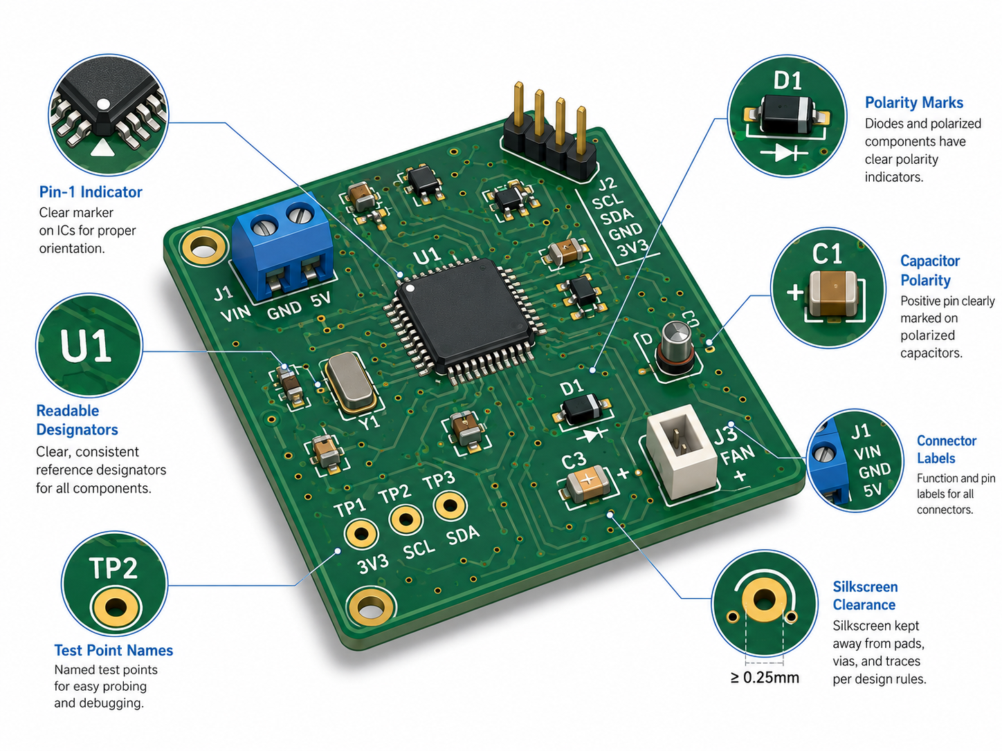
For production boards, the most valuable silkscreen content is the information that prevents assembly errors, wiring mistakes, test confusion, and traceability gaps.
Common Reasons Why PCB Silkscreen Is Missing
A PCB missing silk screen can come from design files, CAM processing, manufacturing limitations, or production control issues. The root cause must be identified before deciding whether the boards can be accepted, reworked, or remade. The most common reasons that causes PCB silkscreen missing including:
| Cause | What Usually Happens | How to Prevent It |
|---|---|---|
| Silkscreen Gerber layer not exported | Entire legend layer is absent | Check Gerber output before release |
| Top and bottom overlay layers confused | Markings appear on the wrong side or disappear | Review layer mapping in CAM |
| Silkscreen placed over pads | CAM removes the text automatically | Keep sufficient clearance from exposed pads |
| Text too small | Characters become unreadable or broken | Follow factory minimum text height and line width |
| Wrong polarity in Gerber data | White or clear areas are inverted | Use Gerber viewer and confirm polarity |
| Solder mask color conflict | Low contrast makes markings look missing | Choose suitable ink color |
| Ink adhesion issue | Text fades, peels, or becomes patchy | Control curing, cleaning, and ink quality |
| Registration shift | Text moves away from target area | Calibrate printing process |
| Dense layout without cleanup | Labels overlap or become clipped | Clean silkscreen during DFM review |
A common engineering mistake is treating silkscreen as the last cosmetic step. In reality, silkscreen should be reviewed during layout, DFM, and first article inspection.
Missing Silkscreen vs. Poor Silkscreen vs. Wrong Silkscreen
These three problems are different and should not be handled the same way.
| Issue | Meaning | Typical Risk | Severity |
|---|---|---|---|
| Missing silkscreen | Marking is absent | Slower assembly, unclear orientation, traceability gap | Medium to high |
| Poor silkscreen | Marking exists but is blurred, faded, or clipped | Misreading and inspection delay | Medium |
| Wrong silkscreen | Marking is printed but incorrect | Wrong assembly, wrong repair, serious quality escape | High |
Wrong silkscreen can be more dangerous than no silkscreen. If a diode polarity mark is absent, an operator may stop and verify the drawing. If the polarity mark is printed incorrectly, the operator may trust the board and assemble the component in the wrong direction. This is why silkscreen verification should be part of engineering release, not only final appearance inspection.
PCB Silkscreen Materials and Printing Colors
Most PCB silkscreen is printed with epoxy-based or UV-curable ink. White is the most common color because it provides strong contrast on green, blue, red, black, and purple solder mask. Black silkscreen is common on white solder mask and some aluminum PCB LED boards.
| Solder Mask Color | Common Silkscreen Color | Readability |
|---|---|---|
| Green | White | Excellent |
| Blue | White | Very good |
| Red | White | Very good |
| Black | White | Good, but glare should be checked |
| White | Black | Excellent |
| Yellow | Black | Good |
| Matte black | White or light gray | Good if ink thickness is stable |
For high-end industrial boards, the ink must remain readable after reflow soldering, cleaning, conformal coating, handling, and long-term service. If the PCB will pass through harsh cleaning, coating, potting, or thermal cycling, the manufacturer should confirm ink adhesion and marking durability before mass production.
Design Rules to Prevent Missing Silkscreen
Good silkscreen design starts before Gerber export. Engineers should not wait until CAM asks for confirmation.
A practical design checklist includes:
- Keep silkscreen away from pads, exposed copper, fiducials, tooling holes, and solder mask openings.
- Use readable text size and line width based on the PCB factory’s capability.
- Place reference designators close to the correct component.
- Avoid placing important labels under components.
- Mark pin 1 clearly for ICs, connectors, modules, and BGAs.
- Mark polarity for diodes, LEDs, tantalum capacitors, electrolytic capacitors, and polarized connectors.
- Use consistent text orientation, preferably one or two reading directions.
- Remove duplicate or non-critical labels on very dense boards.
- Add assembly drawings when the physical board cannot carry all markings.
- Review top and bottom silkscreen separately in a Gerber viewer.
For compact boards, especially HDI PCB, RF modules, wearable electronics, and high-density SMT designs, full reference designators may not fit. In that case, engineers should keep critical polarity and pin-1 marks on the board, then provide a clean assembly drawing for the rest.
Manufacturing Controls for PCB Missing Silkscreen
A reliable PCB manufacturer should check silkscreen during CAM review and production inspection. The goal is not just to print what the customer sent, but to identify conflicts before they become production defects.
Key manufacturing controls include:
- CAM check for missing top or bottom overlay files
- Automatic clearance check between silkscreen and solder mask openings
- Review of minimum character height and line width
- Confirmation of ink color against solder mask color
- First article inspection after printing
- AOI or visual inspection for missing, broken, shifted, or unreadable text
- Ink curing control
- Adhesion and rub resistance checks when required
- Final outgoing quality inspection against Gerber and customer drawing
For OEM and ODM batch production, these checks should be included in the quality plan. If the product requires traceability, revision control, UL marking, QR code, serial code, or customer logo, the approved artwork should be controlled as part of engineering documentation.
Quality Standards and Compliance Considerations
PCB silkscreen is connected to several design, acceptability, and traceability expectations. IPC-A-600 is widely used as an acceptability reference for bare printed boards, while IPC classes help define the quality level expected for the end product.
IPC-2221 is also relevant because it establishes generic design requirements for organic printed boards and is used together with sectional standards for detailed PCB design. For assembly acceptability, manufacturers often refer to related standards such as IPC-A-610 and IPC J-STD-001 according to project requirements.
For commercial products, regulatory and safety markings may also matter. RoHS, FCC, CE, E-waste, and UL-related markings are commonly found on market-ready PCB designs. UL marking may be associated with fabrication and assembly requirements under relevant UL standards.
How Missing Silkscreen Creates Real Production Problems?
A missing silkscreen defect should be analyzed by risk, not only by appearance. The following failure paths are common in real PCB and PCBA production.
| Failure Path | Example | Result | Prevention |
|---|---|---|---|
| Wrong orientation | Missing diode cathode mark | LED, diode, or protection circuit fails | Add clear polarity mark and assembly drawing |
| Wrong IC placement | Missing pin-1 indicator | MCU, driver IC, or memory assembled incorrectly | Use footprint pin-1 mark and package orientation note |
| Wrong connector wiring | Missing connector labels | Cable connected to wrong port | Add connector name and pinout marks |
| Slow debugging | Missing test point labels | Engineers spend extra time probing | Mark key test points such as GND, VCC, RESET, TX, and RX |
| Traceability gap | Missing revision or date code | Mixed board versions in stock | Add revision and lot code |
| Repair error | Missing reference designators | Wrong component replaced | Use clear reference designators or service drawing |
| Inspection delay | Missing labels near high-density parts | FAI takes longer | Provide assembly drawing and centroid file |
This is why a missing silkscreen issue should be reviewed together with BOM, assembly drawing, polarity report, pick-and-place file, test plan, and product application.
How to Decide Whether a PCB Missing Silk Screen Can Be Accepted?
A PCB missing silk screen should not be accepted or rejected automatically. The decision depends on product class, assembly method, application risk, customer requirement, and missing content.
| Missing Content | Prototype Risk | Mass Production Risk | Typical Decision |
|---|---|---|---|
| Decorative logo only | Low | Low | Usually acceptable |
| Non-critical reference designators | Low to medium | Medium | Accept with assembly drawing if approved |
| Polarity mark | Medium | High | Correct or formally approve with controls |
| Pin-1 indicator | Medium | High | Correct before mass production |
| Connector label | Medium | Medium to high | Correct if installation depends on it |
| Test point label | Low to medium | Medium | Add if FCT or repair needs it |
| Revision or date code | Medium | High | Correct if traceability is required |
| UL or compliance mark | High | High | Do not ignore; confirm requirement |
| Safety warning | High | High | Correct before shipment |
For samples, customers may accept missing non-critical silkscreen to save time. For batch production, the safer decision is to correct the artwork before release.
Cost Factors Related to PCB Silkscreen
Silkscreen is usually a small part of PCB fabrication cost, but it can still affect total project cost when it causes rework, delays, scrap, or repeated engineering communication.
Cost factors include:
- Single-side or double-side silkscreen
- Standard white or custom color ink
- Board size and panel quantity
- Printing method
- Fine text and dense layout requirements
- QR code, serial number, or variable data printing
- Special durability requirements
- Rework or remake caused by missing or incorrect markings
- Engineering time spent on DFM correction
The lowest-cost approach is not to remove silkscreen blindly. The better approach is to keep essential markings, remove non-critical clutter, and confirm manufacturability before production.
Supplier Selection Tips for Preventing Silkscreen Problems
When choosing a PCB or PCBA supplier, do not only ask whether they can print silkscreen. Ask how they control silkscreen quality.
A good supplier should be able to answer:
- What is your minimum silkscreen text height and line width?
- What clearance do you require from pads and vias?
- Do you check silkscreen-to-solder-mask conflict during CAM?
- Can you support double-sided silkscreen?
- Can you print QR codes, date codes, or serial numbers?
- How do you inspect missing, blurred, shifted, or broken legend?
- Can you provide DFM feedback before fabrication?
- Can you support both PCB fabrication and PCBA assembly review?
- How do you control revision changes for repeat orders?
For turnkey PCBA projects, the supplier should review silkscreen together with BOM, pick-and-place file, Gerber, assembly drawing, test plan, and quality requirement. This gives better protection than checking each file separately.
PCB Silkscreen Checklist Before Ordering
Before sending files for PCB fabrication or turnkey PCBA, review the silkscreen with this checklist:
| Check Item | Why It Matters |
|---|---|
| Top and bottom silkscreen layers exported | Prevents missing entire legend layer |
| Gerber viewer review completed | Confirms what the factory will see |
| Pin-1 marks visible | Reduces IC orientation errors |
| Polarity marks clear | Protects diodes, LEDs, and capacitors |
| Reference designators readable | Helps inspection and repair |
| Connector labels included | Reduces wiring and installation mistakes |
| Test points labeled | Speeds up debugging and FCT |
| Revision and date code included | Supports traceability |
| Text not placed on pads | Prevents CAM deletion or soldering issues |
| Text size meets factory capability | Prevents broken or unreadable marks |
| Assembly drawing matches silkscreen | Prevents conflicting instructions |
| Customer logo and compliance marks approved | Avoids artwork disputes |
| Final PDF or image proof reviewed | Gives purchasing and engineering teams shared confirmation |
This checklist is especially useful for prototypes that will later move into batch production. It reduces avoidable artwork changes and improves the chance of a smooth production ramp.
FAQs About PCB Missing Silk Screen
1. Is a PCB missing silk screen still usable?
Yes, a PCB missing silk screen may still be usable if the copper circuit, solder mask, drilling, plating, surface finish, and dimensions are correct. The main issue is not electrical conductivity but production usability. Without markings, assembly, inspection, repair, and traceability become harder. For prototypes, it may be accepted with documentation. For mass production, it should be reviewed carefully.
2. Can missing silkscreen cause a PCB to fail?
Missing silkscreen does not usually cause direct electrical failure because it is not part of the circuit. However, it can cause indirect failure if assemblers install polarized components in the wrong direction, connect cables incorrectly, or test the wrong point. For LEDs, diodes, electrolytic capacitors, connectors, ICs, and power input areas, missing markings can create real PCBA failure risk.
3. Why did my PCB manufacturer remove some silkscreen text?
Manufacturers often remove or clip silkscreen when it overlaps exposed pads, solder mask openings, fiducials, or other areas where ink should not be printed. Text may also disappear if it is too small for the process. This is not always a production mistake. Sometimes CAM cleanup protects solderability. The best prevention is reviewing the Gerber output and following the factory’s silkscreen capability rules.
4. Is silkscreen required for all PCBs?
No, not every PCB requires full silkscreen. Very small boards, dense HDI boards, RF modules, and some fully automated assemblies may use minimal markings. However, critical information such as pin-1 marks, polarity marks, connector identification, revision codes, and safety warnings should not be removed without review. The decision should depend on assembly process, product class, traceability needs, and service requirements.
5. What is the difference between PCB silkscreen and solder mask?
Solder mask is the protective coating that covers copper and helps control soldering areas. Silkscreen is the printed legend layer that shows text, symbols, component labels, and other readable information. Solder mask affects insulation and solderability. Silkscreen mainly supports assembly, inspection, testing, and maintenance. They are separate layers in PCB manufacturing files.
6. What information should never be missing from PCB silkscreen?
The most important markings are pin-1 indicators, polarity marks, connector labels, key test point labels, revision identification, and safety warnings. For regulated or controlled products, compliance and traceability marks may also be required. Decorative logos are less important. If board space is limited, prioritize markings that prevent wrong assembly, wrong wiring, wrong testing, or traceability confusion.
7. What is the best silkscreen color for PCB readability?
White silkscreen is the most common choice for green, red, blue, black, and purple solder mask. Black silkscreen is often used on white solder mask. The best color depends on contrast, surface finish, lighting, coating, and customer appearance requirements. For industrial boards, readability is more important than decoration. Always confirm the solder mask and ink combination before production.
8. Should reference designators be printed for every component?
Not always. On dense SMT boards, printing every reference designator can make the silkscreen crowded and unreadable. It is better to prioritize critical parts, connectors, ICs, test points, and polarized components. For very compact boards, reference designators can be moved to an assembly drawing. The goal is not to print more text. The goal is to provide useful production guidance.
9. What should I do if I receive PCBs with missing silkscreen?
Compare the received boards with the approved Gerber files, fabrication drawing, and purchase order requirements. Identify whether the missing information is cosmetic, assembly-related, traceability-related, or compliance-related. If it affects polarity, pin 1, safety, revision control, or required marking, contact the supplier immediately. For urgent prototypes, you may accept with added documentation. For production, request corrective action.