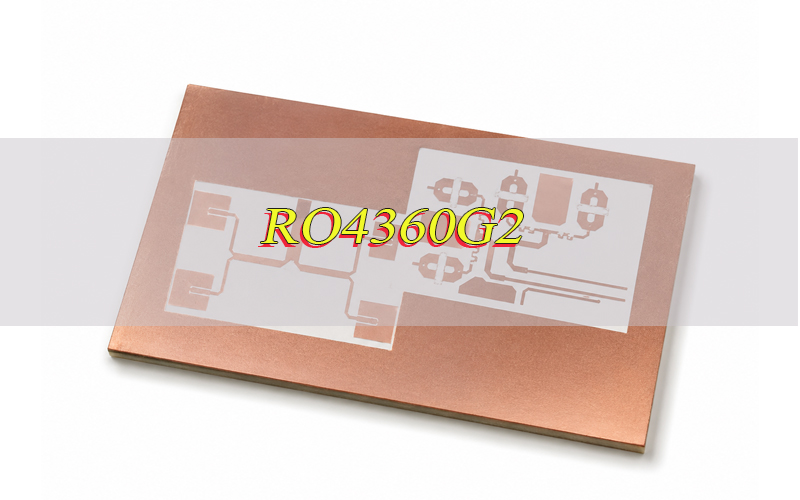
Are you looking for a high-frequency laminate for smaller, more stable, and easier-to-manufacture RF circuit boards? RO4360G2 is a Rogers high-frequency laminate designed for RF applications that need stable dielectric performance, low signal loss, compact circuit size, and reliable PCB fabrication. With its high dielectric constant, low dissipation factor, good thermal behavior, and FR-4-like processing, RO4360G2 is widely used in power amplifiers, small cell transceivers, patch antennas, radar circuits, and other high-frequency boards. This article explains its material properties, datasheet values, applications, design factors, manufacturing process.
What Is RO4360G2?
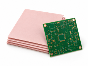
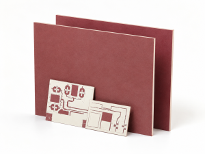
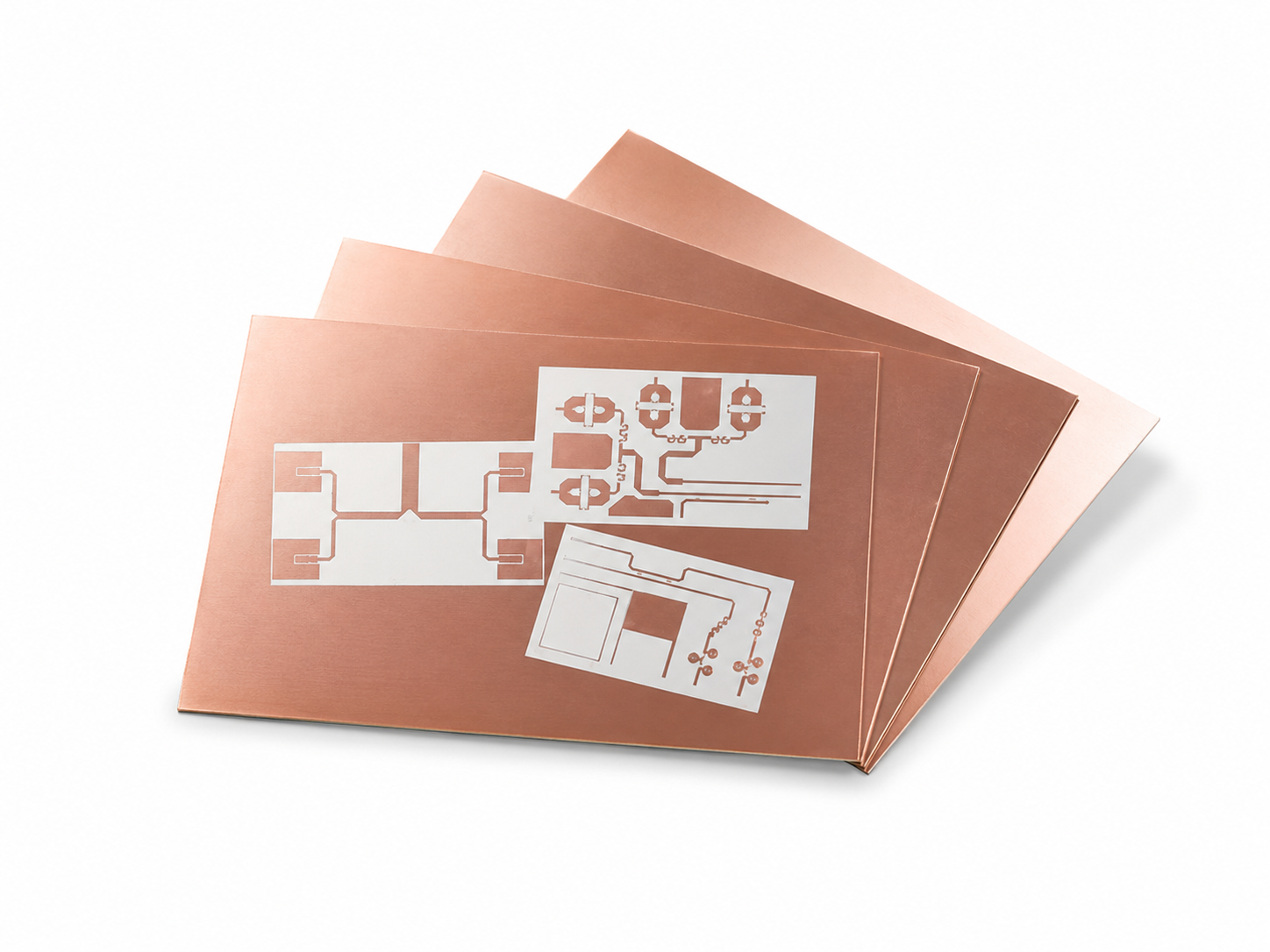
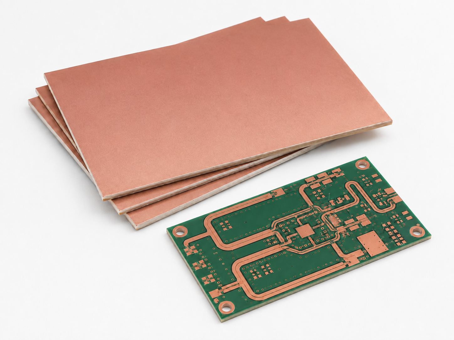
RO4360G2 is a high-frequency circuit material from Rogers Corporation’s RO4000® laminate family. It is a low-loss, glass-reinforced, hydrocarbon ceramic-filled thermoset laminate designed for RF and microwave circuit applications. Rogers lists the material with a process Dk of 6.15 ± 0.15 and a design Dk of 6.4, which helps reduce circuit dimensions when board size and cost matter.
Unlike many PTFE-based RF materials, RO4360G2 is designed for easier fabrication. Rogers states that it processes similarly to FR-4 and supports automated assembly, while also offering low loss, high thermal conductivity, low Z-axis CTE, and lead-free process compatibility.
In RF circuit board manufacturing, RO4360G2 is commonly selected for:
- RF power amplifier boards
- Small cell transceiver PCBs
- Patch antenna circuits
- Ground-based radar boards
- Compact RF modules
- Communication system boards
- Multilayer high-frequency PCB designs
For RF projects, RO4360G2 offers a strong balance between RF performance and manufacturing practicality. It supports compact high-frequency design while keeping fabrication more manageable than many specialty RF substrates.
RO4360G2 High-Frequency Laminates Datasheet
The RO4360G2 high-frequency laminates datasheet provides the main electrical, thermal, mechanical, and processing data needed for RF PCB material selection and fabrication planning. It helps confirm whether the laminate is suitable for the required frequency range, impedance target, board thickness, copper weight, and assembly process. Below is a table and attached PDF file for RO4360G2 for your reference:
| Property | Description |
|---|---|
| Material Type | Glass-reinforced, hydrocarbon ceramic-filled thermoset laminate |
| Material Series | Rogers RO4000® Series |
| Process Dielectric Constant | 6.15 ± 0.15 |
| Design Dielectric Constant | 6.4 |
| Dissipation Factor | 0.0038 at 10 GHz |
| Thermal Conductivity | 0.75 W/m·K |
| X-axis CTE | 13 ppm/°C |
| Y-axis CTE | 14 ppm/°C |
| Z-axis CTE | 28 ppm/°C |
| Tg | >280°C |
| Water Absorption | 0.08% |
| Density | 2.16 g/cm³ |
| Flammability Rating | UL94 V-0 |
| Standard Thicknesses | 0.008”, 0.016”, 0.020”, 0.024”, 0.032”, 0.060” |
| Non-Standard Thickness Range | 0.008” to 0.060”, available in 0.004” increments |
| Copper Cladding Choices | 1/2 oz and 1 oz electrodeposited copper |
| Multilayer Compatibility | Can be paired with RO4400™ prepreg and lower-Dk RO4000 laminates |
| Processing Method | Similar to FR-4 processing |
| Lead-Free Process Compatibility | Yes |
| Common Uses | Power amplifiers, small cell transceivers, patch antennas, radar circuits, RF modules |
Before starting a RO4360G2 circuit board project, the datasheet should be reviewed together with the stackup, impedance requirements, copper thickness, dielectric spacing, surface finish, and assembly conditions. This helps ensure the selected laminate matches both the RF performance target and the fabrication process.
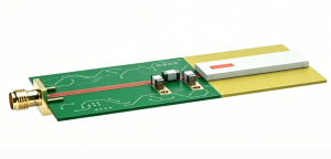
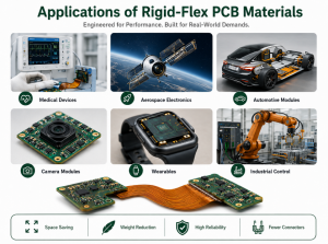
What Are Applications of RO4360G2?
RO4360G2 is used in RF and microwave circuits where compact size, stable electrical behavior, and practical board construction are important. Rogers lists base station power amplifiers, small cell transceivers, patch antennas, ground-based radar, and general RF applications as typical use cases. Here are applications of RO4360G2:
- Base Station Power Amplifiers
- Small Cell Transceivers
- Patch Antennas
- Ground-Based Radar
- Communication System Boards
- Compact RF Modules
How Does RO4360G2 Compare to Other High-Frequency Laminates?
RO4360G2 is often compared with FR-4, PTFE-based laminates, and other Rogers high-frequency materials. The right material depends on frequency, circuit size, insertion loss target, stackup structure, and production cost.
Compared with standard FR-4, RO4360G2 is much better suited for RF applications. FR-4 is widely used for general electronics, industrial control boards, consumer products, and many digital circuits. However, RF designs often need more stable dielectric behavior and lower signal loss. RO4360G2 is designed for high-frequency circuit applications and still processes similarly to FR-4, which gives it a practical manufacturing advantage.
Compared with PTFE-based high-frequency laminates, RO4360G2 offers easier processing. PTFE materials can provide strong RF performance, but they often need more specialized handling during drilling, hole preparation, lamination, and plating. Rogers describes RO4360G2 as a lower total PCB cost solution than competing PTFE products while offering low loss and high thermal conductivity.
| Comparison Item | RO4360G2 | FR-4 | PTFE-Based RF Laminate |
|---|---|---|---|
| RF Suitability | Suitable for many RF and microwave designs | Better for general electronics | Suitable for advanced microwave designs |
| Dielectric Constant | High Dk, 6.15 process value | Varies and not RF-focused | Depends on material grade |
| Circuit Size | Supports compact RF structures | Larger RF structures may be required | Depends on Dk |
| Fabrication | Similar to FR-4 | Standard PCB process | Often more process-sensitive |
| Cost Position | Balanced RF performance and manufacturability | Economical for standard PCBs | Often higher material and process cost |
| Common Use | RF amplifiers, antennas, radar, small cells | Digital and control circuits | Advanced RF and microwave circuits |
The comparison does not mean that one laminate is always better. Each material has a suitable use case. RO4360G2 is a strong material choice when the project needs compact RF geometry, stable high-frequency properties, reliable manufacturing, and reasonable production cost.
Why Use Rogers RO4360G2 for High-Frequency Circuit Boards?
Rogers RO4360G2 is used for high-frequency circuit boards because it brings together high Dk, low loss, good thermal behavior, FR-4-like processing, lead-free compatibility, and multilayer design flexibility.
The high Dk is especially helpful for compact RF layouts. When the dielectric constant is higher, RF traces and resonant structures can often become smaller. This can help reduce board size or leave more space for other components. Rogers notes that RO4360G2, with Dk of 6.15 and design Dk of 6.4, allows circuit dimensions to be reduced where size and cost are critical.
The low dissipation factor helps maintain signal quality. In RF circuit boards, material loss directly affects signal transmission. A lower Df supports better energy transfer across RF traces, matching networks, antennas, and amplifier sections.
Thermal behavior also matters. RO4360G2 has a listed thermal conductivity of 0.75 W/m·K, which supports heat transfer better than many standard PCB materials. For power amplifier boards and dense RF modules, this can help improve thermal performance at the board level.
Another reason to use this material is production efficiency. Since RO4360G2 processes similarly to FR-4, PCB factories with high-frequency material experience can produce it with a more controlled process flow. This can help reduce production complexity compared with some PTFE materials.
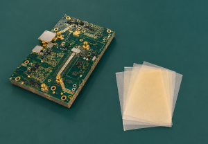
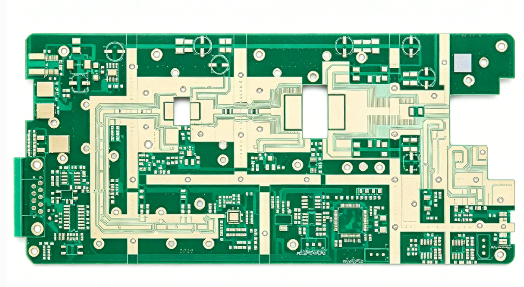
RO4360G2 also supports multilayer RF circuit board design. It can be paired with RO4400™ prepreg and lower-Dk RO4000 laminate in multilayer constructions. This gives the stackup more flexibility for RF, power, and control circuits within the same PCB.
What Are the Design Considerations for RO4360G2 RF Circuit Boards?
A RO4360G2 RF circuit board should not be treated like a standard FR-4 board with a different material name. The design should consider RF behavior, material thickness, copper roughness, impedance control, thermal path, via structure, and assembly process from the beginning.
- Stackup Planning: The stackup should be confirmed before layout finalization. Dielectric thickness, copper weight, prepreg type, and reference plane distance all affect impedance. For multilayer boards, RO4360G2 may be used on selected RF layers while other compatible materials support power or control sections.
- Controlled Impedance: RF trace width depends on Dk, dielectric thickness, copper thickness, solder mask condition, and trace geometry. Microstrip, stripline, and coplanar waveguide structures should be calculated and reviewed before production.
- Copper Selection: Copper type and surface roughness can affect insertion loss at high frequency. For RF boards, copper selection should match the frequency range and loss target.
- Via Design: Via transitions can introduce discontinuities in RF paths. Ground vias, via fences, back drilling, and controlled via spacing may be required depending on the frequency and layout.
- Solder Mask Clearance: Solder mask can change impedance on exposed RF traces. Many RF designs require careful solder mask opening around transmission lines, antennas, and tuning structures.
- Thermal Path: Power amplifier and radar circuits may generate concentrated heat. Thermal vias, copper areas, metal backing, and heat-spreading structures should be reviewed early.
- Panelization and Routing: RF boards may be sensitive to edge accuracy, board flatness, and dimensional tolerance. Panel design should consider routing, breakaway tabs, fiducials, and inspection requirements.
- Surface Finish: ENIG, immersion silver, and other finishes may be selected depending on solderability, RF performance, storage condition, and assembly process. The final choice should match both electrical and manufacturing needs.
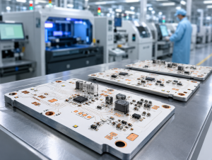
How Is RO4360G2 High-Frequency PCB Manufactured?
RO4360G2 high-frequency PCB manufacturing needs careful control of material, stackup, trace accuracy, and impedance. Although this laminate can be processed similarly to FR-4, RF boards still require tighter fabrication control because small changes in dielectric thickness, copper width, or plating can affect signal performance.
1. Material and Stackup Confirmation
Before production, the manufacturer should confirm the RO4360G2 laminate grade, dielectric thickness, copper weight, finished board thickness, and layer structure. For multilayer RF PCBs, the stackup must also match the impedance requirement and assembly conditions.
2. CAM and DFM Review
The production team reviews Gerber files, drill files, impedance notes, solder mask openings, via structures, and RF trace areas. This step helps find possible manufacturing risks before fabrication starts, such as narrow spacing, unsuitable via design, unclear impedance values, or solder mask issues near RF lines.
3. Imaging and Etching Control
RF traces require accurate line width and spacing. During imaging and etching, the factory must control copper compensation, etching speed, and trace tolerance. This is especially important for microstrip, stripline, and coplanar waveguide designs.
4. Lamination for Multilayer Boards
For multilayer RO4360G2 PCBs, the laminate, prepreg, copper layers, and inner circuits are bonded under controlled temperature and pressure. Stable lamination helps maintain board flatness, layer alignment, and dielectric consistency.
5. Drilling and Copper Plating
Drilling quality affects plated through-hole reliability. The factory should use suitable drilling parameters and then control hole cleaning, copper deposition, and copper plating thickness. Good hole quality helps improve reliability during assembly and long-term use.
6. Solder Mask and Surface Finish
Solder mask must follow the RF design requirement. In some RF areas, solder mask clearance is needed to avoid changes in impedance. The surface finish should also match the soldering process, RF performance needs, and storage requirements.
7. Testing and Final Inspection
After fabrication, the boards should go through electrical testing, AOI, visual inspection, dimensional inspection, and impedance testing when required. For RF projects, inspection records and impedance reports help confirm that the finished PCB matches the design intent.
In short, RO4360G2 PCB manufacturing is not only about producing the board shape. It is about keeping the material, stackup, trace geometry, hole quality, and impedance under control from the first technical review to final shipment.
Why Choose EBest for Your RO4360G2 Circuit Board Manufacturer?
Choosing EBest for your RO4360G2 circuit board means working with a PCB manufacturer that understands RF material control, impedance accuracy, and high-frequency PCB production. This helps reduce design-to-production risk and makes the manufacturing process more predictable. EBest can support your RO4360G2 project with:
- Rogers Material Confirmation: We help confirm laminate grade, dielectric thickness, copper weight, stackup, and surface finish before production. This reduces the risk of material mismatch and specification errors.
- RF Stackup and Impedance Review: Our team reviews stackup structure, trace width, dielectric spacing, copper thickness, and impedance notes to help the board meet the intended RF performance.
- DFM Review Before Fabrication: We check Gerber files, drill files, solder mask openings, via structures, spacing, and RF trace areas before manufacturing. This helps find potential issues early and avoid costly revisions.
- Controlled High-Frequency PCB Manufacturing: EBest controls imaging, etching, lamination, drilling, plating, solder mask, surface finish, and final inspection to support stable RO4360G2 PCB quality.
- Prototype and Small-Batch Support: We support 1 piece prototype and small-batch production, helping verify RF performance, assembly fit, and manufacturability before larger production.
- PCB Fabrication and PCBA Assembly: EBest can provide bare PCB fabrication, component sourcing, SMT assembly, through-hole assembly, and inspection support when a one-stop solution is needed.
- Testing and Quality Records: We can support electrical testing, AOI, visual inspection, dimensional checks, impedance testing, and related quality documentation based on project needs.
If you need RO4360G2 circuit board manufacturing, send your Gerber files, stackup, impedance requirements, BOM, quantity, and delivery target to sales@bestpcbs.com. EBest will review your project and provide practical manufacturing support from PCB fabrication to PCBA assembly.
FAQs About RO4360G2 High-Frequency Laminates
Q1: Which RF products usually benefit from RO4360G2?
A1: RO4360G2 is suitable for RF and microwave circuit boards used in base station power amplifiers, small cell transceivers, patch antennas, radar circuits, communication systems, and compact RF modules.
Q2: What dielectric value should be used during circuit planning?
A2: Rogers lists RO4360G2 with a process dielectric constant of 6.15 ± 0.15 and a design Dk of 6.4. The design value is commonly used during circuit calculation and simulation.
Q3: Can this laminate work in a hybrid multilayer stackup?
A3: Yes. RO4360G2 can be paired with RO4400™ prepreg and lower-Dk RO4000 laminates in multilayer constructions, making it useful for RF, power, and control sections in one PCB.
Q4: Is this material easier to fabricate than PTFE-based RF laminates?
A4: In many cases, yes. Rogers describes RO4360G2 as a thermoset laminate that processes similarly to FR-4, while many PTFE-based materials need more specialized handling.
Q5: What files should be prepared before requesting a quotation?
A5: It is helpful to prepare Gerber files, drill files, stackup drawings, impedance requirements, material notes, surface finish requirements, BOM if assembly is needed, quantity, and delivery target.
Q6: Which inspections are useful for this type of RF PCB?
A6: Common inspection steps include AOI, electrical testing, visual inspection, dimensional checks, and impedance testing when required. For stricter projects, material confirmation and production records may also be useful.
Q7: Can EBest support both bare PCB fabrication and assembly?
A7: Yes. EBest can support RO4360G2 bare PCB fabrication, component sourcing, SMT assembly, through-hole assembly, inspection, and related testing support based on the project requirement.