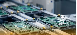
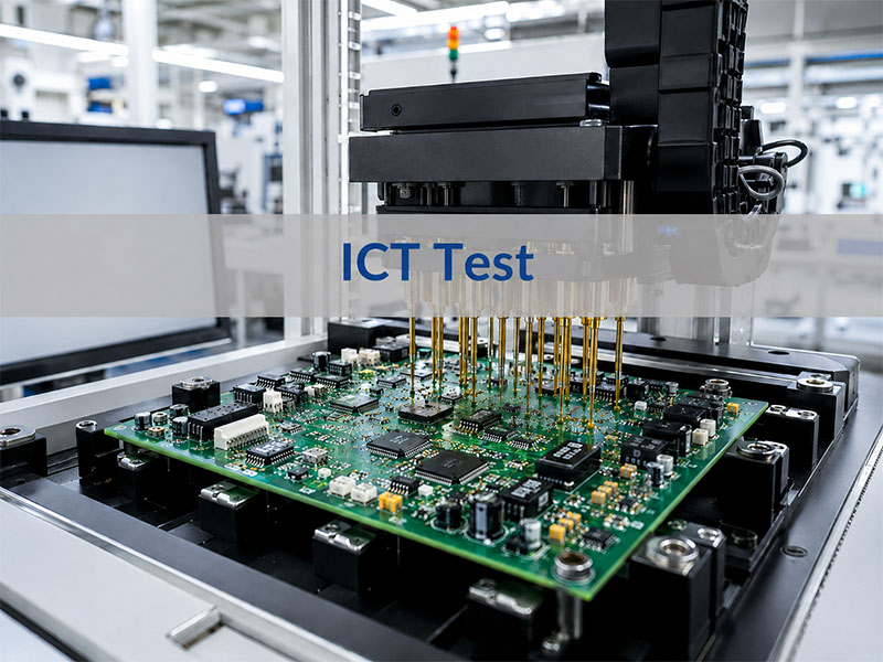
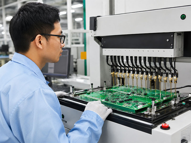
An ICT test helps PCB assembly manufacturers check circuit quality before boards move to final inspection or shipment. During PCBA production, small defects can hide under components, inside solder joints, or between fine-pitch pads. Visual inspection may miss them. AOI may also miss some electrical faults. Therefore, in-circuit testing gives engineers a faster and more direct way to check whether the assembled PCB matches the design. In this guide, you will learn what ICT testing means, how the process works, why test points matter, and how ICT compares with FCT and flying probe testing.
What Is an ICT Test in PCB Assembly?
An ICT test, or In-Circuit Test, checks an assembled PCB at the component and circuit level. Manufacturers usually use it after SMT assembly, DIP soldering, reflow soldering, or wave soldering.
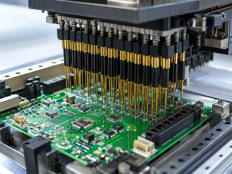
During the test, spring-loaded probes touch selected test points on the PCB. These probes connect the board to an ICT tester. Then, the tester measures electrical values and checks whether the circuit matches the expected design.
In simple words, ICT testing checks whether the PCB assembly was built correctly.
What Does ICT Testing Confirm?
ICT testing can check many basic assembly conditions. For example, it can confirm whether components sit in the right locations. It can also check whether solder joints create a stable electrical connection.
In addition, it helps engineers find:
- Short circuits
- Open circuits
- Wrong component values
- Missing components
- Reversed diodes or capacitors
- Poor solder joints
- Incorrect IC pin connections
- Basic power rail problems
As a result, ICT testing gives manufacturers a clear view of board-level assembly quality.
Why Is ICT Important for PCBA Quality?
ICT does more than separate pass and fail boards. It also helps engineers find process trends.
For example, if many boards fail at the same resistor, the issue may come from placement, solder paste, component supply, or PCB pad design. Therefore, the test result can guide process improvement.
This makes ICT useful for both inspection and manufacturing control.
Why Is ICT Test Done During PCBA Manufacturing?
Manufacturers perform ICT testing to find assembly defects early. This is important because early detection saves time, reduces rework, and improves final product quality.
If a board reaches functional testing with many basic faults, engineers may spend more time troubleshooting. However, ICT can detect many of these faults before the final test stage. Therefore, the whole production flow becomes smoother.
ICT Helps Find Defects Earlier
Many PCBA defects start at the assembly stage. Some defects come from solder paste printing. Others come from placement, reflow, component polarity, or PCB design.
ICT can find common defects such as:
- Solder bridges
- Open solder joints
- Wrong resistors
- Missing capacitors
- Reversed diodes
- Lifted IC pins
- Shorts between power and ground
- Poor contact on important nets
Because ICT checks the board at the circuit level, it can find problems that visual inspection may not reveal.
ICT Reduces Troubleshooting Time
A functional test may show that a board does not work. However, it may not show the exact reason.
ICT gives more specific information. It can point to a certain net, component, pin, or test point. As a result, engineers can locate the failure faster.
For example, FCT may show that a control board cannot power on. ICT may show that a power rail has a short. This saves time and makes repair work more efficient.
ICT Supports Stable Mass Production
ICT testing works especially well for medium- and high-volume PCBA production. Once engineers complete the fixture and test program, operators can test each board quickly.
This creates a repeatable standard for every production batch. Moreover, the factory can collect failure data and monitor process stability over time.
Therefore, ICT is not only a test method. It also supports long-term quality management.
What Does an ICT Tester Check on a PCB?
An ICT tester checks whether the assembled PCB matches the expected electrical design. The exact coverage depends on the board layout, test points, fixture quality, and test program.
In most cases, the tester checks component values, circuit continuity, short circuits, and basic semiconductor behavior. It may also check some powered circuits, depending on the product and fixture design.
Common ICT Test Items
| ICT Test Item | What It Checks | Typical Defects Found |
|---|---|---|
| Open Circuit Test | Whether a circuit path has a proper connection | Broken trace, poor solder joint, missing connection |
| Short Circuit Test | Whether two nets connect by mistake | Solder bridge, copper residue, layout issue |
| Resistance Test | Whether the resistor value matches the design | Wrong resistor, missing resistor, poor soldering |
| Capacitance Test | Whether the capacitor value stays within range | Wrong capacitor, missing capacitor, polarity issue |
| Diode Test | Forward and reverse behavior | Reversed diode, wrong diode, poor contact |
| Transistor Test | Basic semiconductor behavior | Wrong part, weak soldering, wrong mounting |
| IC Pin Test | Pin connection and basic response | Lifted pin, solder bridge, poor wetting |
| Polarity Check | Orientation of polarized components | Reversed diode, reversed capacitor |
| Power Net Check | Power rail condition | Short on power line, unstable connection |
What ICT Cannot Fully Check
ICT is powerful, but it does not replace every other test. For example, it may not fully check firmware, wireless communication, display behavior, motor control, or sensor response.
Therefore, many manufacturers combine ICT with FCT. ICT checks the circuit build quality. Then, FCT checks whether the board works in its real application.
This combined method gives better quality coverage.
How Does the ICT Test Procedure Work?
The ICT test procedure starts before production testing. Engineers need to review files, define test points, design the fixture, build the test program, and debug the setup.
A clear process helps improve test coverage and reduce false failures. Moreover, it helps the factory prepare for stable production.
Step 1: Review PCB Design Files
First, engineers review the Gerber files, BOM, schematic, netlist, assembly drawing, and test requirements.
This review helps them understand the circuit structure. It also helps them decide which nets and components need testing.
At this stage, engineers may also find layout issues that affect test access.
Step 2: Define ICT Test Points
Next, engineers check the test point layout. Each important net should have a clear and reachable test point.
Good test points help the fixture contact the PCB with stable pressure. In contrast, poor test points may reduce coverage and create false failures.
Therefore, test point review should happen before mass production.
Step 3: Design the ICT Fixture
After that, the fixture team designs the ICT test fixture. The design depends on board size, panel layout, test point locations, component height, and board thickness.
The fixture must hold the PCB firmly. It must also align the probes with the test points accurately.
Good fixture design improves test stability and reduces repeat test issues.
Step 4: Develop the Test Program
The test program tells the ICT tester what to measure. It also defines the acceptable range for each test item.
For example, the program may include resistance limits, capacitance tolerance, diode voltage range, and short/open limits.
A well-built program helps the tester judge each board consistently.
Step 5: Debug and Verify the Setup
Before mass production, engineers debug the fixture and program with sample boards.
During this stage, they check probe contact, adjust limits, and remove false failures. They also compare ICT results with actual board conditions.
Once the setup becomes stable, the production team can start routine testing.
Step 6: Run Production Testing
During production, operators place each PCBA into the fixture and start the test. The tester then gives a pass or fail result.
If the board fails, the team separates it for repair or engineering review. Meanwhile, pass boards move to the next process.
This keeps the production flow organized.
Step 7: Analyze Failure Data
Finally, engineers review ICT failure data. If the same fault appears many times, they investigate the root cause.
The issue may come from stencil design, solder paste volume, placement accuracy, reflow profile, component quality, or PCB layout.
Therefore, ICT data can help improve the whole assembly process.
What Are ICT Test Points and Why Do They Matter?
ICT test points are exposed copper pads or contact areas on a PCB. Test probes touch these points during in-circuit testing.
Without good test points, even a strong ICT tester cannot deliver high coverage. Therefore, test point design plays a major role in PCBA testability.
Why Test Points Affect Coverage
Every important circuit net needs access. If a net has no test point, the ICT fixture may not check it directly.
As a result, test coverage drops. Also, the test may miss certain open circuits or weak connections.
Good test points help the fixture contact the board reliably. They also reduce false failures caused by poor probe contact.
Key ICT Test Point Design Tips
| Design Factor | Practical Recommendation |
|---|---|
| Test Point Size | Make the pad large enough for stable probe contact |
| Spacing | Keep enough clearance between nearby test points |
| Solder Mask Opening | Expose a clean copper area for the probe |
| Location | Avoid tall parts, board edges, and blocked zones |
| Distribution | Spread points evenly when possible |
| Surface Finish | Choose a finish that supports stable contact |
| Accessibility | Prefer one-side access when the layout allows it |
| Mechanical Support | Add support pins when probe force may bend the board |
When Should Engineers Plan Test Points?
Engineers should plan ICT test points during PCB layout. This timing matters.
If the team thinks about ICT after the design is complete, changes may become harder. The customer may need to revise the layout, delay production, or accept lower test coverage.
Therefore, DFM review should include testability review. This is especially important for products that will enter repeat production.
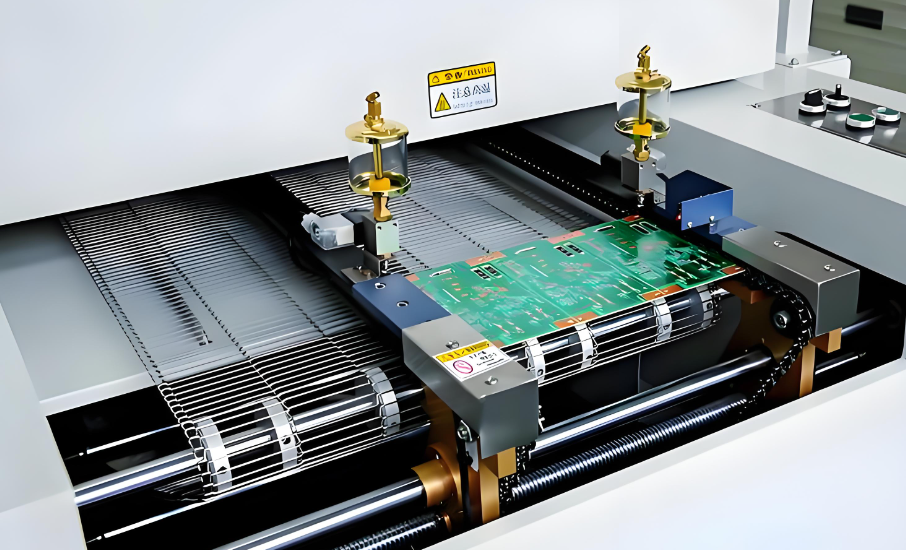
What Is an ICT Test Fixture?
An ICT test fixture connects the assembled PCB to the ICT tester. Many people also call it a “bed-of-nails” fixture because it uses many spring-loaded probes.
The fixture positions the board, aligns the probes, and creates electrical contact with the test points. Without a reliable fixture, ICT results may become unstable.
Main Parts of an ICT Fixture
A typical ICT fixture may include:
- Probe plate
- Spring-loaded pogo pins
- Alignment pins
- Board support pins
- Press structure or vacuum structure
- Interface wiring
- Connector interface
- Board positioning frame
- Safety cover
Each part helps the fixture contact the PCB accurately and safely.
Why Custom Fixture Design Matters
Manufacturers design each ICT fixture for a specific PCB or panel. Therefore, fixture design must match the actual product.
Several factors affect the fixture:
| Factor | Why It Matters |
|---|---|
| PCB Size | It affects fixture structure and board support |
| Panel Design | It affects probe layout and handling efficiency |
| Test Point Count | More points require more probes and wiring |
| Component Height | Tall parts need enough fixture clearance |
| Board Thickness | Thin boards may need extra support |
| Probe Side | Single-sided probing is simpler than double-sided probing |
| Production Volume | High-volume products need durable fixtures |
How a Good Fixture Improves Testing
A good fixture improves contact stability. It also reduces false failures and repeat testing.
For example, if the fixture does not support the board well, probe pressure may bend the PCB. Then, some probes may lose contact. This can create false failures.
Therefore, fixture debugging is a key step before mass production.
ICT Test vs FCT Test: What Is the Difference?
ICT and FCT both support PCBA quality control. However, they check different things.
ICT checks how the board was assembled. FCT checks how the board works.
Because of this difference, many manufacturers use both methods in one test strategy.
ICT vs FCT Comparison
| Item | ICT Test | FCT Test |
|---|---|---|
| Full Name | In-Circuit Test | Functional Circuit Test |
| Main Purpose | Check assembly quality and circuit connectivity | Check final product function |
| Test Level | Component and net level | System or application level |
| Test Method | Probes contact PCB test points | Board runs in a simulated working condition |
| Fixture Type | Bed-of-nails fixture | Functional test jig |
| Common Defects Found | Opens, shorts, wrong values, missing parts, reversed parts | Firmware issues, communication failure, power-up problems, signal errors |
| Test Speed | Fast after setup | Depends on product function |
| Best Use Case | Medium- and high-volume PCBA production | Product-level verification |
| Main Limitation | It does not fully check real-world operation | It may not locate component-level faults quickly |
When Should You Use ICT and FCT Together?
For many products, the best answer is not ICT or FCT. Instead, the better option is ICT plus FCT.
First, ICT checks whether the circuit was assembled correctly. Then, FCT checks whether the product performs its intended function.
This approach works well for industrial control boards, medical electronics, communication modules, automotive electronics, LED control boards, and power control products.
As a result, the manufacturer can catch both assembly-level faults and function-level issues.
Flying Probe Test vs ICT Test: Which One Should You Choose?
Flying probe testing and ICT testing both check electrical conditions on a PCB assembly. However, they suit different production stages.
A flying probe test uses moving probes. It does not need a dedicated bed-of-nails fixture. Therefore, it works well for prototypes and small batches.
ICT uses a custom fixture. Because of that, it offers faster testing for stable and higher-volume production.
Flying Probe vs ICT Comparison
| Item | Flying Probe Test | ICT Test |
|---|---|---|
| Fixture Requirement | No dedicated fixture | Custom fixture required |
| Setup Cost | Lower | Higher initial fixture cost |
| Test Speed | Slower | Faster |
| Flexibility | High | Lower after fixture completion |
| Best For | Prototype and small-batch production | Medium- and high-volume production |
| Design Changes | Easy to adapt | Fixture may need modification |
| Unit Cost in Volume | Higher | Lower after fixture cost spreads across volume |
| Test Coverage | Good for accessible nets | Strong when test points are well designed |
When Flying Probe Makes More Sense
Flying probe testing is a good choice for prototypes. It also works well when the PCB design may still change.
At this stage, the customer may only need a few boards. In that case, building a custom ICT fixture may not make sense.
In addition, flying probe testing gives engineers more flexibility during early product development.
When ICT Makes More Sense
ICT becomes more attractive when the design becomes stable. It also works better when the order quantity increases.
Although the fixture has an initial cost, the test speed is much faster. Over many boards, the cost per unit becomes more reasonable.
Therefore, ICT often fits repeat orders, stable PCB assemblies, and mass production.
Simple Selection Guide
| Project Situation | Better Choice |
|---|---|
| Prototype only | Flying probe |
| Small batch with frequent design changes | Flying probe |
| Stable design with repeat orders | ICT |
| Medium-volume production | ICT |
| High-volume production | ICT |
| Need fast fault location in production | ICT |
| No proper test points | Flying probe may be more practical |
In practice, the best test method depends on product complexity, order volume, layout condition, and reliability needs.
FAQs About ICT Test
1. Can ICT testing find every PCBA defect?
No. ICT testing can find many circuit-level and component-level defects. However, it cannot check every real operating function.
For better coverage, manufacturers often combine ICT with FCT, AOI, X-ray inspection, and visual inspection.
2. Is an ICT fixture worth the cost for small batches?
Usually, an ICT fixture fits stable and repeat production better. For prototypes or small batches, flying probe testing may offer better value.
However, if the product will move into mass production soon, early ICT planning can still help.
3. What affects ICT test coverage?
ICT test coverage depends on test point access, PCB layout, component type, fixture design, probe contact, and test program quality.
Therefore, engineers should review testability during the DFM stage.
4. Why do some boards fail ICT even when they look correct?
Some defects are not easy to see. For example, a solder joint may look good but still have weak electrical contact.
Also, a component may sit in the correct location but have the wrong value. ICT helps detect these hidden issues.
5. Can ICT testing replace functional testing?
No, in most cases. ICT checks circuit assembly quality. FCT checks whether the board works in its final application.
Therefore, both methods often work together in a complete PCBA test plan.
6. When should ICT test points be designed?
Engineers should design ICT test points during PCB layout. This gives the layout team more freedom to place clear and stable test pads.
If the team waits until production, changes may cost more time.
7. What is the difference between ICT test pins and ICT test probes?
In daily production, people often use these two terms in a similar way. They usually refer to the spring-loaded contact parts inside the test fixture.
These probes touch the PCB test points during testing.
8. How does ICT testing help PCBA manufacturers improve quality?
ICT testing gives fast and detailed failure data. Engineers can use this data to find repeated issues and improve the process.
For example, they may adjust stencil design, placement settings, reflow profile, or test point layout.
9. Should every PCB assembly project use ICT testing?
Not every project needs ICT. The right choice depends on product complexity, order quantity, budget, and reliability needs.
For stable medium- or high-volume PCB assemblies, ICT is often a strong and practical choice.