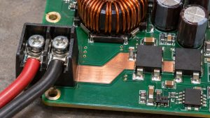
PCB infrared temperature measurement needs a defined surface and measurement setup, not just a thermal camera pointed at the board. Shiny copper can emit little infrared radiation while reflecting its surroundings. A cool-looking copper path may therefore be hotter than it appears, and a bright patch may be a reflection rather than a local heat source.
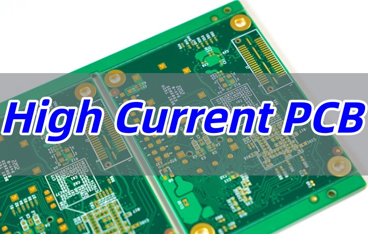
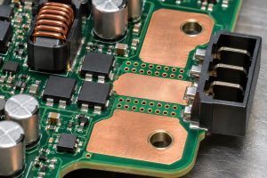
Consider a hypothetical high-current prototype with exposed copper beside green solder mask. An engineer wants to check its conductor temperature under the approved load. This guide follows the measurement review before any layout decision; it does not provide permission to energize, probe or modify an unsafe circuit.
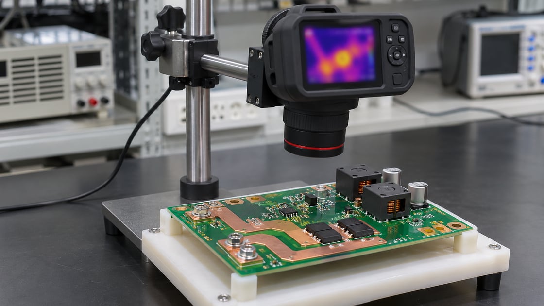
What the Camera Measures at a Copper Surface
The camera detects radiation reaching its sensor and uses a model to estimate surface temperature. For an opaque surface, emitted and reflected contributions both matter; the reading is not a direct electrical measurement of the copper.
On the teaching board, exposed copper and adjacent solder mask can have different radiative behavior even where their actual temperatures are close. First identify exactly which visible surface the measurement region covers. A number taken across copper, mask and a component body is not automatically the temperature of any one of those objects.
Record the Parameters Behind a Temperature Reading
A credible result preserves the camera, surface, optical setup and operating condition together. A cropped color screenshot without these inputs is incomplete.
| Parameter | Unit or record | Why it matters |
| Emissivity | Dimensionless, 0–1 model scale | Relates radiation to the surface |
| Reflected apparent temperature | °C, method stated | Accounts for reflected surroundings |
| Camera and lens | Model, calibration, spectral band | Defines measurement capability |
| Geometry | Distance, angle, target size | Defines what is resolved |
| Operating state | A, V, duration and airflow | Defines the heat-producing condition |
| Target | Surface, location and board revision | Prevents comparing different objects |
The table specifies reporting fields, not universal settings. Use the actual camera’s instructions and a qualified test plan to establish values. Do not insert a guessed emissivity simply because another board had the same color.
Compare Bare Copper, Solder Mask and a Reference Patch
These surfaces cannot be compared as if one camera setting makes all of them equally reliable. Their finish, optical properties and thermal relationship to the conductor differ.
| Surface | Main concern | Useful check |
| Shiny copper | Low emission, strong reflection | Validate the surface method |
| Solder mask | Different surface from copper | Identify coating and target |
| Known reference patch | Compatibility and equilibration | Verify material and thermal contact |
| Component package | Surface is not the junction | Use component-specific limits |
FLIR’s emissivity explanation notes that highly polished copper or aluminum commonly has emissivity below 0.10. That is a warning about reflective surfaces, not a calibrated value for this prototype. Plating, oxidation, roughness and wavelength can change the appropriate value.
Distinguish Emissivity from Thermal Conductivity
Emissivity concerns radiation from a surface; thermal conductivity concerns heat transfer through a material. Copper can conduct heat well while remaining difficult to measure by infrared imaging.
For the high-current path, do not conclude that a cool-colored area has low electrical loss or strong cooling simply because it is copper. Conversely, a dark high-emissivity patch does not make the underlying material a better heat conductor. Keep the thermal model, electrical loss estimate and radiometric measurement as related but separate pieces of evidence.
Check Reflections Before Calling a Bright Patch a Hotspot
A reflective surface can redirect radiation from nearby people, equipment or other warm objects into the camera. Its apparent temperature can then differ from its actual surface temperature.
Record the surroundings and viewing geometry. A feature that changes strongly with the viewing arrangement warrants investigation before it is labeled a fault; changing the view alone does not quantify the correct temperature. In the teaching review, keep people and movable heat sources from changing the scene during the comparison. Do not reach into an energized assembly to test a reflection hypothesis.
Use a Reference Patch Only Under an Approved Method
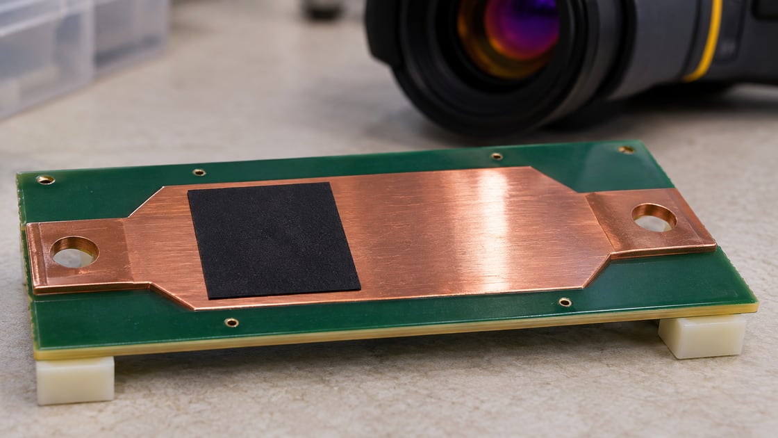
A known high-emissivity patch can make a difficult surface easier to observe, but only when its optical behavior, temperature suitability and thermal relationship are understood. Any preparation must occur under the appropriate safe, de-energized procedure.
FLIR’s reference-material guidance warns that tape can transmit infrared radiation and that emissivity depends on wavelength and surface condition. Not every black tape is a characterized reference. Do not apply coatings indiscriminately to live conductors, fine-pitch contacts, optical parts or contamination-sensitive areas.
Verify the Patch Follows the Target Temperature
The patch must be in adequate thermal contact and allowed to reach the relevant condition; otherwise the camera is accurately reading the wrong surface temperature. A patch also changes the surface being tested.
FLIR’s Extech infrared-measurement FAQ instructs users to let the reference material adjust to the surface temperature. For the prototype, consider whether a large or thick patch changes local heat transfer, bridges distinct areas or lags a short pulse. Keep any modified test specimen identifiable and avoid presenting it as an untouched production assembly.
Check Focus and the Smallest Target Size
A visible feature is not necessarily large enough for a trustworthy temperature measurement. The lens, working distance and optical blur determine how much surrounding material contributes to the reported point.
FLIR’s electronics macro-imaging discussion illustrates why a measurement target needs adequate pixel coverage and suitable optics. Use the actual camera’s measurement specification rather than assuming one illuminated pixel is sufficient. On our board, a narrow copper neck can be blended with cooler surroundings even when its location is apparent on screen.
Keep Load, Airflow and Timing Comparable
Temperature comparisons need the same defined operating condition. Different current, elapsed time, enclosure state or airflow can change the result independently of the copper geometry.
For the hypothetical prototype, record the approved load and whether the objective is a steady condition or a transient event. Opening an enclosure for the camera can alter cooling; document that boundary instead of treating the exposed bench result as a closed-product result. Do not improvise overload tests or infer a safe current rating from a single cool-looking frame.
Use Contact Measurements as an Independent Check
An appropriate contact sensor can help investigate a disputed infrared reading, but it has its own attachment, heat-flow and electrical-safety limitations. It is a cross-check, not an automatic truth source regardless of installation.
The two methods must address the same physical location and comparable time state. A sensor on a package top cannot validate a camera reading on a distant copper region, and neither directly measures an inaccessible semiconductor junction. If the methods disagree, review both setups before averaging the values or choosing the more convenient result.
Do Not Confuse Palette Contrast with Thermal Severity
Color maps depend on the selected range and palette; the brightest spot is not necessarily an unacceptable temperature. A different scale can make the same dataset look more or less dramatic.
Compare actual validated values, uncertainty and applicable limits, not color alone. Save the original radiometric data where the instrument supports it, together with the settings and visible-light context. A compressed screenshot may preserve the appearance while losing the ability to inspect measurement regions or revise justified analysis parameters.
Make a Layout Decision Only After the Measurement Is Defensible
A thermal image can direct the investigation, but it does not by itself identify electrical resistance, current distribution or the failure cause. Link the observation to the circuit and independent evidence.
- Identify the surface and the exact test point.
- Confirm optics, focus and target coverage.
- Establish emissivity and reflection treatment.
- Record load, airflow and timing.
- Cross-check critical temperatures with a suitable method.
- Compare against the correct component or conductor requirement.
The related high-current PCB neck-down guide explains one possible electrical heating mechanism. Investigate it when the geometry and loss evidence support that explanation, not merely because a thermal palette highlights the area.
FAQ
Can I use 0.95 for every part on a PCB?
No. A single convenient setting does not characterize shiny metal, coatings and package materials equally. Use a verified surface method and the camera’s relevant instructions. A general material table can help identify a concern, but it is not calibration evidence for every finish, wavelength band, temperature and observation angle on the board.
Does a higher-resolution camera eliminate emissivity error?
No. More pixels can improve spatial detail, but they do not identify how the surface emits and reflects radiation. Focus, optics and target size still matter as well. Treat spatial resolution and radiometric interpretation as separate requirements; an exceptionally sharp picture of reflective copper can still carry a misleading temperature estimate.
Can the camera see a hot inner-layer trace through the board?
Ordinary PCB thermal imaging shows the observed surface response, not a direct view through an opaque stackup to each internal conductor. Internal heating can influence surface temperature, but that does not uniquely identify its source. Use construction information, electrical evidence and an appropriate thermal model before attributing the surface pattern to one hidden trace.
Can digital zoom make a narrow conductor measurable?
Digital enlargement does not add optical information that the sensor never resolved. It can make an image easier to view while leaving the original target coverage unchanged. Check the camera and lens measurement capability, focus and working distance. Do not mistake a large on-screen pixel block for a newly resolved physical temperature feature.
Will a visible-light photo tell me the infrared emissivity?
No. Appearance in visible light does not establish optical behavior in the camera’s infrared band. A finish that looks dark or matte may still need characterization, and surface condition can vary. Use the appropriate material evidence or validated method rather than choosing a setting solely from a color photograph of the board.
Does a cool connector prove its contact resistance is acceptable?
No. The observed surface may be reflective, unresolved or thermally separated from the critical contact. Load and elapsed time also affect the result. Validate the temperature measurement and apply the relevant electrical and mechanical acceptance checks. A cool-looking connector image cannot replace contact-resistance evidence or establish the condition of a hidden joint.
Can I compare before-and-after boards using different automatic palettes?
Not by color intensity alone. Record comparable operating conditions and measurement settings, then compare validated temperatures at defined locations. An automatically rescaled image can exaggerate or conceal a difference. Preserve the underlying data and scale information so the comparison remains meaningful even if a presentation palette is later changed.
Does a checked surface temperature establish a semiconductor junction temperature?
Not automatically. The junction is inside the device, and the relationship to a measured surface depends on the package, heat paths and operating condition. Use the manufacturer’s appropriate characterization or validated thermal model. Do not compare a copper-surface reading directly with a junction-temperature limit and call the device qualified.
For a Best Technology high-current PCB enquiry, send the conductor construction, operating condition and defined temperature-validation scope to sales@bestpcbs.com. Distinguish calculated loss, observed surface temperature and verified assembly performance in the review package.