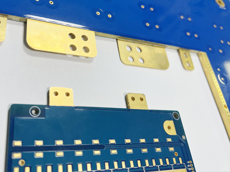
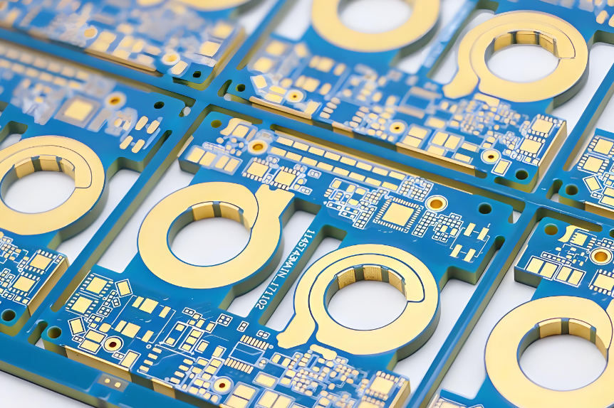
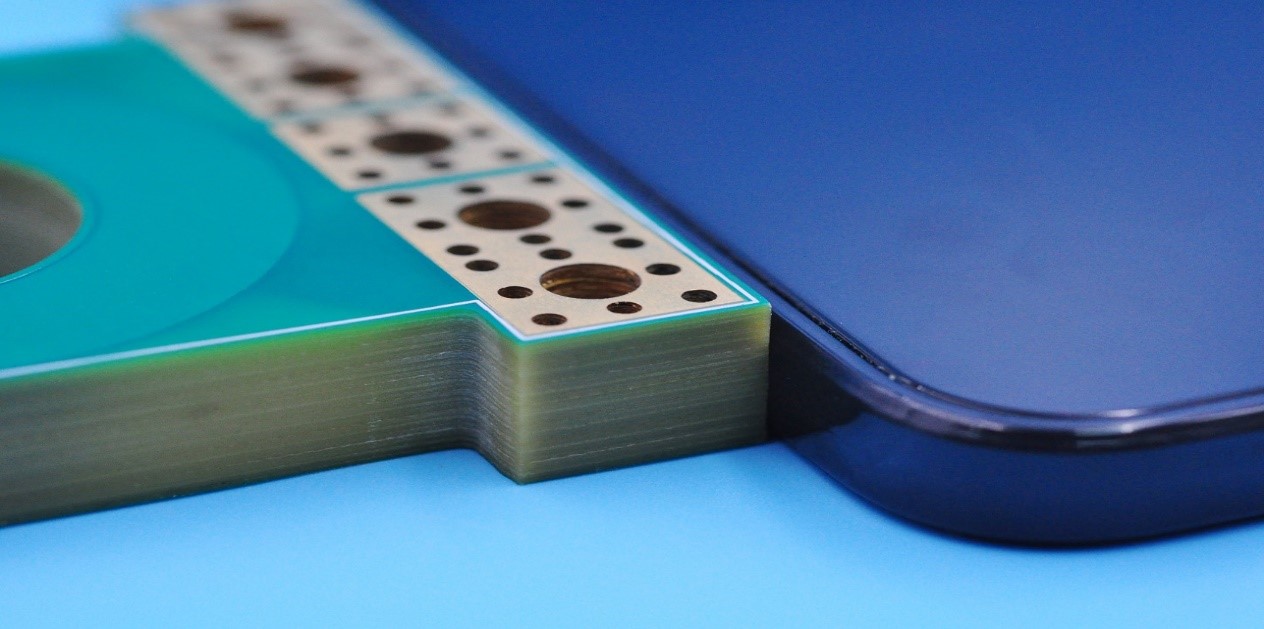
Buyers comparing heavy copper PCB manufacturers in Israel can approach verified Israeli fabricators, Israel-based engineering and sourcing providers, or qualified overseas factories. PCB Technologies and Eltek publicly identify PCB manufacturing operations in Israel and describe thick-copper or heavy-copper capability. APEX PCB and Ma’agalim D.S. are useful Israel-based contacts, but buyers should confirm which factory will manufacture each order.
The purchasing decision should follow a clear sequence: identify realistic suppliers, check whether the relevant factory has suitable certifications, compare the complete process capability, verify quality evidence, and then normalize price, lead time, and supply terms. This prevents a local address, a broad “heavy copper” claim, or a low quotation from being mistaken for a qualified manufacturing solution.

Which Heavy Copper PCB Manufacturers Are Available in Israel?
Buyers evaluating heavy copper PCB manufacturers in Israel can begin with two verified Israeli fabricators and two Israel-based engineering or sourcing providers. Separating these roles at the shortlist stage shows who is responsible for fabrication and which companies require further confirmation of the production site.
| Company | Address | Services | Process capabilities | Lead time | Advantages |
|---|---|---|---|---|---|
| PCB Technologies | 7 Ahoman St., Migdal-HaEmek, Israel, as stated on its published site certificate | PCB fabrication, PCB assembly, testing, inspection, rework, NPI, and offshore coordination | Multilayer high-reliability PCBs, thick copper, embedded copper, via farms, thermal management, HDI, rigid-flex, and prototype through low- or mid-volume production | Project-specific; confirm after DFM, material review, capacity allocation, inspection scope, and the selected local or offshore route | Israeli fabrication identity with PCB and PCBA support; useful when the project needs close engineering coordination across board, assembly, and thermal requirements |
| Eltek | 20 Ben Zion Gelis St., Petach Tikvah 4927920, Israel | High-reliability PCB engineering and in-house fabrication, with global sourcing available for additional production routes | Heavy-copper multilayers, HDI, rigid, flex, rigid-flex, RF and microwave, special materials, and high-reliability constructions | Project-specific; confirm the quick-turn slot, material availability, engineering-release date, tests, and whether Eltek or a sourcing partner will build the order | Direct access to an Israeli high-reliability manufacturer; relevant when aerospace, defense, medical, RF, or complex multilayer controls influence qualification |
| APEX PCB | Kibbutz Hazorea 3658100, Israel | Local technical support and PCB sourcing through a global supplier network | Published heavy-copper range above 70 µm up to 204 µm, plus multilayer, rigid-flex, HDI, IMS, and high-frequency PCB options | Project-specific; depends on the assigned factory, material, stackup, quantity, inspection, international transport, and customs | Israeli point of contact with access to multiple production options; useful when local coordination is needed and the actual factory remains transparent |
| Ma’agalim D.S. | 22 Maskit St., Herzliya 46733, Israel | PCB layout, fabrication sourcing, assembly, simulation, panelization, and turnkey project coordination | High-Tg heavy-copper foil, multilayer, HDI, rigid-flex, metal-base and mixed-dielectric boards, microvias, blind or buried vias, and specialized routing | Project-specific; confirm the production factory, engineering-release point, material plan, inspection scope, and delivered date in Israel | Combines local design and project support with fabrication and assembly coordination; useful when one contact must manage several engineering stages |
The shortlist is ready only when each company’s role, production address, capability scope, and delivery basis are clear. The next filter is whether the factory’s certificates cover the site, process, and end market required by the project.
What Certifications Should You Check When Choosing a Heavy Copper PCB Manufacturer?
Use certification as the first qualification filter by matching the standard to the product and the certificate to the factory that will build the board. Check the legal entity, address, scope, issuing body, certificate number, and validity dates before accepting any certification claim.
- ISO 9001: This is a general quality-management baseline covering controlled processes, records, corrective action, and continual improvement. Confirm that the certificate scope includes PCB fabrication or the operation being purchased.
- IATF 16949: This may be relevant for automotive supply chains that require automotive quality planning, traceability, change control, and defect-prevention systems. Do not request it merely because the board carries high current; its relevance comes from the customer and product program.
- ISO 13485: Medical-device projects may require a quality system designed for regulated medical manufacturing. Check whether the certificate covers the responsible facility and whether the supplier can meet the project’s traceability and change-control requirements.
- AS9100: Aerospace and defense programs may require aerospace quality controls in addition to technical PCB capability. Confirm the certified entity, site, scope, and any customer-specific approval before relying on the claim.
- UL recognition and material compliance: If the design or market requires a UL-recognized PCB construction, RoHS, REACH, or another material declaration, identify the exact requirement in the RFQ. General corporate compliance language does not prove that the released stackup is covered.
A valid, relevant, site-specific certificate allows a supplier to move into technical evaluation; it does not approve the board itself. The next step is to compare whether that certified factory can manufacture the full copper, stackup, geometry, hole, material, and finish combination.
What Heavy Copper PCB Capabilities Should You Compare?
Compare the complete manufacturable feature combination, not the largest copper weight printed on a capability page. Two factories may both advertise 6 oz copper while accepting very different layer counts, finished holes, spacing, materials, or board thicknesses.
- Base and finished copper by layer: State inner- and outer-layer requirements separately. Outer layers normally gain copper during plating, so the starting foil and finished value are not interchangeable. Ask the supplier to mark both values on its proposed stackup.
- Layer count and mixed copper construction: Confirm whether the requested copper can be combined with the total layer count, dielectric structure, overall thickness, and lighter signal layers. Mixed weights can affect etching, resin fill, registration, lamination, and warpage.
- Minimum trace and spacing: Heavy copper requires more etching allowance and changes the achievable conductor profile. Submit the actual narrowest features and copper clearances instead of relying on a standalone minimum value.
- Finished holes and current transitions: Define drilled size, finished size, via structure, barrel-copper requirement, via quantity, and current through each transition. A broad surface conductor can still be limited by a narrow neck, connector pad, or insufficient plated-hole copper.
- Material and board thickness: Confirm the laminate family, Tg or other required properties, dielectric thicknesses, thermal constraints, overall thickness tolerance, and dimensional limits. A listed material may not be available with every heavy-copper construction.
- Surface finish and solder mask: Check whether the selected finish, mask thickness, color, clearance, and assembly interface are compatible with the copper topography and end-use environment.
- High-current design inputs: Provide conductor width and length, continuous and peak current, duty cycle, allowable temperature rise, ambient conditions, airflow, heat sinking, and terminal limits. The factory reviews manufacturability; the product team remains responsible for validating electrical and thermal performance.
A meaningful capability comparison uses the same released construction for every supplier and records all accepted limits or required changes. Once manufacturability is confirmed, the buyer must verify whether the chosen process can repeatedly produce boards that meet the approved requirements.
How Can You Check a Manufacturer’s Heavy Copper PCB Quality?
Ask each qualified supplier to show how it will verify copper thickness, plated holes, materials, dimensions, electrical integrity, and lot release. Defining these records before quotation makes quality measurable and exposes any inspection gaps before production begins.
- Copper-thickness verification: Agree on how inner copper, finished outer copper, and relevant plated features will be measured. For critical designs, request traceable coupon or microsection results tied to the correct part number, revision, panel, and production lot.
- Plated-through-hole evaluation: Specify finished-hole dimensions and the applicable barrel-copper or workmanship requirement. A microsection can show plating distribution, voids, hole-wall condition, and the relationship between the drilled feature and finished result.
- Material traceability: Request laminate, copper foil, surface-finish chemistry, date code, lot identity, and certificate-of-conformance records appropriate to the project. Verify that the received records identify the shipped revision and quantity.
- Dimensional inspection: Define critical board dimensions, overall thickness, slots, hole locations, cutouts, and tolerances. Ask whether the supplier will provide first-article measurements or a lot inspection report for the characteristics that affect fit or current-path assembly.
- Electrical testing: State continuity, isolation, netlist, impedance where applicable, and any special high-current or functional test that must be performed. The report should identify the test method, coverage, revision, and acceptance result.
- First-article and lot release: Use a controlled first build to verify fit, assembly, current path, temperature rise, and product operation. Transfer all approved changes into the fabrication data, stackup, BOM, inspection plan, and test instructions before repeat production.
- Nonconformance and change control: Agree on notification, containment, root-cause response, rework approval, and authorization for factory, material, stackup, or process changes. This is especially important when an Israel-based supplier coordinates an external factory.
The preferred supplier should return a focused set of traceable records proving that the shipped lot matches the approved stackup and acceptance plan. With capability and quality evidence aligned, price can be compared without rewarding a quotation that excludes necessary controls.
What Affects the Price of Heavy Copper PCBs in Israel?
Heavy copper PCB pricing depends on material use, process difficulty, manufacturing yield, inspection scope, order quantity, and the chosen supply route. A credible comparison therefore uses the same stackup, quantities, quality requirements, and delivery terms for every supplier; otherwise, the lowest quotation may describe a different board or a narrower service.
- Copper weight and distribution: More copper increases raw-material use and can add etching, plating, lamination, and process-control demands. Mixed copper weights or uneven copper distribution may also require extra engineering and panel balancing.
- Layer count and board size: More layers increase material, lamination, drilling, imaging, registration, and inspection work. Large boards may reduce panel utilization, while small boards can still be expensive if routing and array requirements waste usable panel area.
- Trace, spacing, and hole structure: Fine features combined with thick copper, small finished holes, buried or blind vias, sequential lamination, controlled depth, or demanding aspect ratios increase process risk and can reduce yield.
- Material and surface finish: High-Tg, low-loss, high-thermal-performance, halogen-free, or tightly controlled laminate systems can cost more than common FR-4. Surface finish, thick mask, edge plating, copper coins, and other special features add separate process steps.
- Quantity and production stage: Prototypes carry setup, tooling, CAM, material, and inspection costs across few boards. A larger repeat order may lower the unit cost, but only after the design, stackup, panel, and process are stable.
- Testing and documentation: Microsections, coupons, impedance records, detailed dimensional reports, material certificates, first-article inspection, special electrical tests, and regulated-industry documentation add work but may prevent much larger downstream losses.
- Local or overseas fulfillment: Compare fabrication, tooling, testing, packaging, freight, insurance, customs, taxes, broker charges, and delivery responsibility. Local coordination can reduce some communication or logistics friction, while an overseas factory may offer a broader process or capacity range.
A comparable quotation uses one revision, one stackup, matching quantities, the same inspection scope, and the same delivered terms. After differences in assumptions, exclusions, one-time charges, and optional services are visible, the buyer can test whether each supplier’s promised schedule covers the same work.
How Long Does Heavy Copper PCB Production Usually Take?
There is no dependable universal lead time for a heavy copper PCB because the schedule begins with engineering release and depends on material, construction, capacity, inspection, and transport. Ask suppliers for a dated schedule with clear assumptions instead of accepting a single turnaround number.
- Prototype stage: The schedule should include file review, engineering questions, stackup approval, material allocation, fabrication, inspection, and shipment. A fast build date is not useful if DFM questions or customer approvals remain outside the quoted clock.
- Small-batch or first-article stage: Allow time to incorporate prototype changes, stabilize tooling and panelization, complete the agreed quality records, assemble or test the product if required, and obtain customer release before increasing quantity.
- Volume-production stage: Repeat orders can become more predictable after the process is frozen, but copper foil, laminate, capacity loading, yield, batch size, documentation, and forecast changes still affect delivery. Confirm whether the stated schedule assumes reserved material or capacity.
- Engineering and material release: Confirm when the clock starts, when DFM questions must close, which stackup requires approval, and whether the specified copper and laminate are already available.
- Fabrication complexity: Ask how mixed copper, multiple laminations, small or controlled holes, unusual thickness, embedded copper, edge plating, and panel yield affect the production plan.
- Inspection and assembly: Include the time required for first-article reports, microsections, electrical tests, PCBA, functional testing, customer review, and any hold point before the next quantity.
- Delivery to Israel: Separate factory completion, inspection release, dispatch, freight, customs clearance, and local delivery so the quoted date has one clear meaning.
A credible lead time identifies the release date, material status, critical process, inspection scope, shipping milestone, and final delivery point. Once every schedule is measured the same way, the buyer can decide whether local manufacturing, overseas production, or a coordinated sourcing route offers the better overall control.
How Do Israeli and Overseas Heavy Copper PCB Suppliers Compare?
Compare Israeli and overseas suppliers on engineering control, process fit, total delivered terms, evidence, logistics, and recovery capability. Geography influences these factors, but it does not determine them automatically.
- Communication and engineering access: A local supplier may simplify time-zone alignment, meetings, or site visits. An overseas manufacturer can still provide effective support when named engineers, response times, drawing control, and escalation routes are agreed before the order.
- Manufacturing capability: Compare the same stackup, copper, geometry, hole, material, finish, size, and volume combination. A nearby factory is not automatically capable of the design, and an overseas factory is not automatically more capable.
- Commercial comparison: Evaluate the total delivered offer, including tooling, inspection, documentation, packaging, shipping, customs responsibility, taxes, minimum order quantity, payment terms, and the effect of prototypes on the production price.
- Lead time and transport: Separate engineering approval, factory production, inspection, dispatch, freight, customs, and local delivery. Local production may shorten the transport segment, while available overseas capacity may shorten manufacturing for some constructions.
- Quality records and traceability: Require the same evidence from both routes. If a local service provider uses another factory, the manufacturing site, certificate, lot identity, test responsibility, and change-control path should remain visible.
- Changes and corrective action: Compare how each supplier manages urgent engineering changes, nonconforming material, replacement builds, failure analysis, and return logistics. Responsibility should be written into the order rather than assumed from location.
- Supply continuity: For continuity-sensitive products, consider qualifying a second source against the same data and acceptance plan. Do not treat two boards as interchangeable until their materials, stackups, copper, plating, finish, testing, and product validation agree.
The stronger supply route is the one that combines process fit with clear ownership of engineering, quality, delivery, and corrective action. After selecting that route, the buyer must convert every quotation assumption into a controlled order package before production is released.
What Should You Confirm Before Placing a Heavy Copper PCB Order?
Before issuing the purchase order, convert every quotation assumption into an approved manufacturing and acceptance requirement. This final release check should produce one controlled order package that both the buyer and supplier can identify without relying on email history.
- Freeze the data revision: Confirm the Gerber or ODB++ package, Excellon files, netlist, fabrication drawing, panel or array drawing, and revision. The quotation, DFM response, and purchase order should reference the same identity.
- Approve the stackup: Record material, dielectric thicknesses, base and finished copper by layer, overall thickness, surface finish, solder mask, controlled impedance, and any special construction. Resolve differences between the customer stackup and factory proposal in writing.
- Close manufacturing questions: Confirm minimum trace and spacing, copper clearance, finished holes, slots, via types, barrel requirements, board dimensions, tolerances, current transitions, and any approved deviations.
- Define inspection and release: State workmanship criteria, electrical test, dimensional checks, coupon or microsection requirements, certificates, traceability, first-article records, sampling, and acceptance limits.
- Confirm quantity and production stage: Separate prototype, first-article, small-batch, and repeat quantities. Identify whether a sample approval is required before the supplier buys material or releases the next quantity.
- Lock delivery and commercial terms: Confirm the delivery destination, Incoterm, freight method, packaging, customs responsibility, shipment date definition, payment terms, tooling ownership, and validity of the quotation.
- Approve change control: Require written authorization before changes to material, stackup, copper, tooling, manufacturing site, subcontractor, process, test method, or released data. Name the contacts responsible for technical and quality decisions.
- Add the PCBA package when required: Include the BOM, approved alternatives, placement data, assembly drawing, soldering constraints, firmware, programming instructions, fixtures, functional test, pass/fail limits, and enclosure or final-assembly requirements.
The order is ready when both parties reference the same data, stackup, factory, inspection plan, quantity, commercial terms, and change-control rules. These requirements also provide a fair basis for deciding whether EBest Circuit’s overseas manufacturing model fits the Israeli project.
Why Choose EBest Circuit for Heavy Copper PCB Supply to Israel?
EBest Circuit is a China-based PCB and PCBA manufacturer serving Israeli projects; it is not a PCB manufacturer in Israel. It is an overseas option for buyers who want engineering review, fabrication, component sourcing, assembly, and agreed testing coordinated through one supplier.
- Fewer manufacturability surprises: A design-specific review covers stackup, inner- and outer-layer copper, conductor geometry, plated transitions, material, finish, and mechanical constraints. Israeli customers can resolve open points before material and production commitments are made.
- Lower transfer risk: Prototype, controlled first-build, and mass-production support can use the same released PCB data, BOM, and test requirements. Approved changes remain visible when the project moves to a larger quantity.
- One coordinated PCB and PCBA workflow: Fabrication files, component sourcing, placement data, assembly drawings, programming instructions, and functional-test limits can be reviewed together. This reduces handoff gaps between the heavy-copper board and the assembly process.
- Quality evidence matched to the order: The supplied company profile lists ISO 9001:2015, IATF 16949, ISO 13485:2016, AS9100D, UL, RoHS, and REACH credentials. Customers can identify the applicable certificate, inspection records, traceability, and acceptance evidence before release.
- Clear international delivery planning: The quotation can separate production, inspection, packaging, shipping, customs responsibility, and delivery to Israel. Written milestones and escalation contacts give the buyer better control over schedule and corrective action.
EBest is most relevant when an Israeli buyer values coordinated engineering, prototype-to-production continuity, documented quality requirements, and a clearly managed overseas delivery route. Send the Gerber or ODB++ data, fabrication drawing, proposed stackup, finished copper by layer, current and thermal requirements, quantities, delivery destination, and acceptance plan to sales@bestpcbs.com for a free DFM review and quotation. The FAQs below clarify the final technical and sourcing questions that commonly affect supplier approval.
FAQs About Heavy Copper PCB Manufacturers in Israel?
Q1: Are there PCB factories in Israel that publicly advertise heavy-copper capability?
A1: Yes, PCB Technologies and Eltek publicly identify Israeli manufacturing and heavy- or thick-copper capability. Each released design still needs a factory-specific DFM review because copper weight alone does not confirm the full construction.
Q2: Is every PCB supplier with an Israeli address an Israeli manufacturer?
A2: No. An Israeli address does not by itself prove local fabrication. Confirm the legal entity, production address, operation performed there, certificate scope, subcontractors, and responsibility for quality before qualification.
Q3: Is 2 oz copper considered a heavy copper PCB?
A3: Supplier terminology varies, so the drawing should control the requirement. Some companies reserve “heavy copper” for finished copper around 3 oz and above, while others group 2 oz with thick or high-copper boards. State the required finished copper on every layer instead of using the category name as the acceptance criterion.
Q4: Are base copper and finished copper the same?
A4: No, base copper and finished copper can differ. Outer layers usually gain copper during through-hole plating, while inner-layer copper is defined differently by the starting foil and processing. Ask the manufacturer to show both values separately on the approved stackup.
Q5: Does heavier copper automatically allow more current?
A5: No. Heavier copper is only one part of the current and temperature-rise calculation. Conductor width and length, ambient temperature, airflow, nearby copper, insulation, connectors, vias, duty cycle, and allowable temperature also matter. Validate the complete current path under the product’s real operating conditions.
Q6: Can heavy copper be combined with fine-pitch circuitry?
A6: Yes, but the exact feature combination requires factory review. Copper thickness, conductor profile, spacing, layer allocation, registration, resin fill, solder mask, and process limits all affect feasibility. Separating high-current and dense-signal features across appropriate layers may improve manufacturability.
Q7: Can an overseas manufacturer supply heavy copper PCBs to Israel?
A7: Yes, provided the overseas factory meets the same technical, quality, and delivery requirements used for local candidates. Compare certification, evidence, communication, shipping, customs responsibility, sample approval, and corrective action with the same released data and total delivery scope.
The final supplier decision should connect factory identity, certification, manufacturability, quality evidence, total delivered terms, and an approved order package. Using the same requirements for every candidate gives the buyer a defensible basis for selecting a local Israeli factory, an Israel-based sourcing provider, or a qualified overseas manufacturer.