PCB manufacturing PCB manufacturing
Home > Blog

PCB Thickness Tolerance: FR4 PCB Thickness Tolerance for Prototype and Production

July 13th, 2026

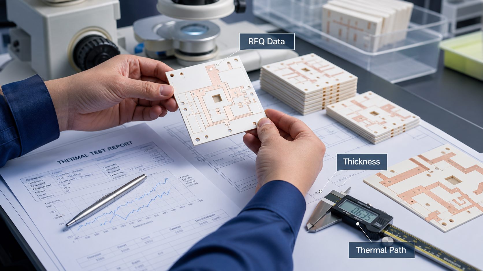
PCB thickness tolerance is one of the most important mechanical requirements in PCB manufacturing. It affects enclosure fit, connector alignment, controlled impedance, heat transfer, assembly stability, and final product reliability. For many engineers, the key question is simple: if the design calls for a 1.6mm FR4 PCB, how close will the finished board be to that number after lamination, copper plating, solder mask, surface finish, and final inspection?

EBest Circuit (Best Technology) supports custom PCB and PCBA projects where finished PCB thickness tolerance must match real product requirements, such as connector fit, housing assembly, impedance control, and prototype-to-production consistency. Our engineering team can review your stackup, material, copper thickness, mechanical drawing, and tolerance notes before production, so board thickness risks are not discovered too late. If you are working on a PCB project with strict thickness requirements, pls feel free to send your Gerber files, stackup, drawings, or questions to sales@bestpcbs.com. We will help you check the practical manufacturing path before the board is built.

PCB Thickness Tolerance

What Is PCB Thickness Tolerance?

PCB thickness tolerance is the allowed variation between the designed board thickness and the actual finished board thickness after manufacturing.

For example, if a PCB is specified as 1.6mm thick with a +/-10% tolerance, the finished PCB thickness may be acceptable within a range of about 1.44mm to 1.76mm. If the project requires a tighter mechanical fit, the drawing may specify a narrower tolerance such as +/-0.10mm, but the feasibility depends on the material, stackup, copper weight, and production process.

PCB thickness tolerance is not only a number on a drawing. It can affect:

  • Connector fit and insertion depth
  • Card-edge contact reliability
  • Enclosure and screw-hole alignment
  • Controlled impedance stackup
  • Thermal performance
  • Mechanical stiffness
  • Assembly yield
  • Product appearance

For simple prototype boards, standard tolerance may be enough. For products with slots, housings, camera modules, medical electronics, automotive modules, or high-speed interfaces, thickness tolerance should be reviewed before production.

FR4 PCB Thickness Tolerance in Manufacturing

FR4 PCB thickness tolerance is the thickness variation of a finished PCB made with FR4 laminate and prepreg. FR4 is the most common PCB base material, but it is not perfectly fixed in thickness. Laminate suppliers, copper foil, resin content, press conditions, and final surface finish can all create variation.

Common FR4 PCB thicknesses include 0.4mm, 0.6mm, 0.8mm, 1.0mm, 1.2mm, 1.6mm, 2.0mm, and 2.4mm. Among these, 1.6mm is the most widely used standard thickness for many rigid PCB applications.

In many standard FR4 PCB manufacturing projects, +/-10% is often treated as a practical reference range. However, this should not be assumed for every board. Thin boards, heavy copper boards, multilayer boards, impedance-controlled boards, and boards that must fit into a precise enclosure may need a different tolerance agreement.

At EBest Circuit, FR4 PCB thickness is reviewed together with the stackup, copper weight, board size, panel arrangement, surface finish, and assembly requirements. This matters because the board the customer receives is the finished PCB, not only the raw laminate.

PCB Board Thickness Tolerance Before and After Production

PCB board thickness tolerance should be considered in two stages: the designed thickness before production and the finished thickness after production.

Before production, the drawing or stackup may define the target board thickness. This can include the core, prepreg, copper layers, and sometimes solder mask or surface finish assumptions. For many products, the target thickness is selected based on standard material availability and mechanical requirements.

After production, the final board thickness can be affected by several process factors:

FactorEffect
CoreBase thickness variation
PrepregResin flow after pressing
CopperAdds stackup height
LaminationChanges dielectric thickness
FinishSmall final surface change

This is why a PCB drawing should clearly state whether the thickness tolerance refers to the finished PCB thickness. If the requirement is only written as “1.6mm PCB” without tolerance, the manufacturer may quote a standard tolerance instead of a tighter one.

Finished PCB Thickness Tolerance and Why It Matters

Finished PCB thickness tolerance refers to the final measured board thickness after all major PCB processes are complete. This is the value that matters most for product assembly.

Finished PCB thickness is especially important when the PCB must connect with:

  • Edge-card connectors
  • FPC or board-to-board connectors
  • Mechanical slots
  • Press-fit parts
  • Screw bosses or plastic housings
  • Heat sinks or thermal pads
  • Optical or sensor modules
  • Shielding cans

If the finished board is too thick, it may not fit the enclosure or connector. If it is too thin, connector contact pressure, stiffness, or vibration resistance may be affected. In high-speed boards, a change in dielectric thickness can also affect impedance.

For this reason, engineering drawings should define the finished PCB thickness tolerance clearly. A good note may include:

Finished PCB thickness: 1.6mm +/-0.10mm, measured after surface finish.

If the tolerance is critical, the manufacturer should review feasibility before production and confirm whether special material selection, stackup control, or process control is needed.

PCB Thickness Tolerance IPC Standards

Many engineers search for PCB thickness tolerance IPC standards because they want a reliable reference. IPC standards are important in PCB manufacturing, but it is risky to assume that one universal IPC number applies to every PCB thickness tolerance case.

IPC documents such as IPC-6012 and IPC-A-600 are commonly used for rigid PCB performance and acceptability requirements. They help define quality expectations, inspection criteria, and acceptance conditions. However, for board thickness, the customer’s drawing, procurement specification, stackup, material selection, and manufacturer capability are still very important.

In practical PCB manufacturing, the safest approach is:

  • Define the target finished PCB thickness.
  • Define the acceptable tolerance.
  • Confirm whether the tolerance applies before or after surface finish.
  • Confirm whether thickness is measured at panel level or finished board level.
  • Ask the PCB manufacturer to review stackup feasibility.

If your project requires IPC Class 2 or Class 3 production, mention it clearly. If your product is used in medical, automotive, aerospace, industrial control, or high-reliability electronics, the thickness tolerance should be part of the full DFM and quality review, not a small note at the end of the drawing.

1.6mm PCB Thickness Tolerance and 62 Mil Boards

The most common PCB thickness is 1.6mm, often also called about 62 mil or 63 mil. The exact conversion is close, but in everyday PCB sourcing, engineers often use 1.6mm and 62 mil as practical equivalents.

A standard 1.6mm FR4 PCB is widely used because it offers a good balance of stiffness, availability, cost, and assembly compatibility. Many manufacturers can support a standard tolerance such as +/-10%, but this may be too wide for products that depend on connector fit, housing slots, card-edge contacts, or precise mechanical positioning.

Engineers may also compare 1.6t vs 1.2 PCB when choosing board thickness. In this context, 1.6t usually means a 1.6mm thick PCB, while 1.2 PCB usually means a 1.2mm thick board. A 1.6mm board is generally stiffer and more common for standard FR4 assemblies, while a 1.2mm board can help reduce product thickness or weight. However, the final choice should depend on enclosure space, connector requirements, mechanical strength, stackup, and the finished PCB thickness tolerance.

For example:

RequirementWhy It Matters
1.6mm +/-10%Common for standard FR4 boards
1.6mm +/-0.15mmBetter for mechanical fit
1.6mm +/-0.10mmNeeds tighter stackup review
1.2mm PCBUseful for thinner products
62 mil card-edge PCBConnector fit should be confirmed

If your product uses a card-edge connector, do not only write “1.6mm PCB”. Confirm the connector datasheet and define the required finished board thickness at the contact area. In some cases, plating, beveling, surface finish, and edge tolerance may also need attention.

Core, Prepreg, and Dielectric Thickness Tolerance in PCBs

PCB thickness tolerance is built from several material layers. For multilayer boards, the final thickness is not only one piece of FR4. It is the result of cores, prepregs, copper layers, lamination, and final processing.

The three key terms are:

TermMeaning
PCB core thickness toleranceVariation in the rigid core material
PCB prepreg thickness toleranceVariation after prepreg resin flows during lamination
PCB dielectric thickness toleranceVariation in insulation thickness between copper layers

Dielectric thickness matters because it affects impedance. If a high-speed design requires 50-ohm single-ended impedance or 90/100-ohm differential impedance, the dielectric thickness cannot be treated casually.

For controlled impedance boards, engineers should provide:

  • Gerber files
  • Stackup requirement
  • Copper thickness
  • Impedance target
  • Reference layers
  • Trace width and spacing
  • Test coupon requirement
  • Impedance test report requirement

EBest Circuit reviews these details during DFM before production. If the required impedance and the requested finished PCB thickness conflict, the stackup may need adjustment before manufacturing begins.

PCB Thickness Tolerance

Multilayer and Flex PCB Thickness Tolerance

Multi-layer PCB thickness tolerance is usually more complex than simple double sided pcb boards. More layers mean more cores, prepregs, copper layers, and lamination variables. A 4-layer, 6-layer, 8-layer, or 10-layer board may require a custom stackup instead of a standard laminate.

For multilayer boards, thickness tolerance affects:

  • Controlled impedance
  • Via aspect ratio
  • Lamination stability
  • Warpage risk
  • Press-fit and connector fit
  • Mechanical strength
  • Thermal path

Flex PCB thickness tolerance is different again. Flexible PCB thickness may include PI film, adhesive, copper foil, coverlay, stiffener, shielding film, and surface finish. A flex PCB may be extremely thin, but connector-end thickness may be built up with FR4 or PI stiffeners.

When comparing multilayer PCB thickness tolerance and flex PCB thickness tolerance, the key question is not only “how thick is the PCB?” It is also:

  • Where is the thickness measured?
  • Is the stiffener included?
  • Is the connector end thicker than the flexible area?
  • Is the board rigid, flex, or rigid-flex?
  • Does the finished product need bending?

For flex and rigid-flex projects, always provide the mechanical drawing. A simple Gerber file is usually not enough to control thickness correctly.

PCB Thickness Tolerance

How to Choose a PCB Manufacturer for Tight Board Thickness Tolerance

If your project needs tight board thickness tolerance, choose a PCB manufacturer that can review the requirement before quoting, not only after production begins.

A reliable PCB manufacturer should be able to check:

  • Target finished PCB thickness
  • FR4 material and laminate availability
  • Stackup feasibility
  • Core and prepreg selection
  • Copper thickness and plating impact
  • Impedance requirements
  • Connector or enclosure fit
  • Warpage and mechanical risk
  • Measurement and inspection method
  • Prototype and production consistency

For high tolerance board thickness projects, communication is as important as manufacturing capability. A small mismatch in drawing notes can lead to a board that is electrically acceptable but mechanically unsuitable.

EBest Circuit supports quick PCB fabrication, component sourcing, PCB SMT assembly, DFM review, BOM optimization, testing, and small-batch or mass production. Our engineering team helps customers check board thickness tolerance together with real product requirements, including enclosure fit, connector requirements, impedance control, and assembly process.

For projects where thickness matters, we recommend sending the Gerber files, stackup, mechanical drawing, connector datasheet, and any finished thickness tolerance requirement before production. This helps prevent rework and shortens the path from prototype to reliable production.

FAQs about PCB Thickness Tolerance

What does PCB dimension tolerance IPC mean?

PCB dimension tolerance IPC usually refers to dimensional quality expectations guided by IPC standards and project drawings. For thickness, outline, holes, and slots, the safest method is to define the exact tolerance on the drawing and ask the PCB manufacturer to confirm feasibility before production.

What is PCB board outline tolerance?

PCB board outline tolerance is the allowed variation in the finished board shape, length, width, or routed edge. It matters when the PCB must fit into an enclosure, slot, camera housing, connector frame, or mechanical fixture.

Is PCB trace width tolerance related to PCB thickness tolerance?

PCB trace width tolerance is not the same as board thickness tolerance, but both can affect impedance. For controlled impedance PCBs, trace width, dielectric thickness, copper thickness, and stackup should be reviewed together.

Why do PCB hole position tolerance and PTH tolerance matter?

PCB hole position tolerance affects how well mounting holes, vias, and connectors align with the product. PCB PTH tolerance affects plated through-hole fit, solderability, and component insertion. Both should be controlled when the PCB has tight mechanical or assembly requirements.

How much PCB board edge clearance should I keep?

PCB board edge clearance depends on routing, copper spacing, voltage, connector location, and enclosure design. As a general rule, keep critical copper, holes, and components away from the routed edge and confirm the clearance with your PCB manufacturer during DFM review.

If you need help with PCB thickness tolerance, FR4 PCB thickness tolerance, 1.6mm PCB tolerance, or a mechanically sensitive PCB project, pls feel free to send your Gerber files, stackup, drawings, and project notes to sales@bestpcbs.com. EBest Circuit can help review your files and recommend a practical manufacturing path before production starts.

You may also like

Custom Multi Layer Printed Circuit Board Manufacturer with Speedy Delivery

July 9th, 2026

Multi layer printed circuit board technology helps engineers place more circuitry, power distribution, signal routing, and ground shielding inside a compact board structure. Compared with a single layer or double-sided PCB, a multilayer PCB gives the designer more routing layers, better electrical control, and more space for complex electronics.

EBest Circuit (Best Technology) supports custom multilayer PCB manufacturing with DFM review, engineering response, material and process review, PCB fabrication, component sourcing, PCBA assembly, testing, and shipment documentation. A warm welcome to send your Gerber files, stack-up notes, quantity, and delivery requirements to sales@bestpcbs.com for an engineering review.

Multi Layer Printed Circuit Board

What Is a Multi Layer Printed Circuit Board?

A multi layer printed circuit board is a PCB made with three or more conductive copper layers laminated together with insulating material. In practical PCB manufacturing, multilayer boards usually start from 4 layers and can increase to 6, 8, 10, 12 layers or more depending on the design.

Each conductive layer can be used for signal routing, power distribution, ground reference, shielding, or controlled impedance structures. The layers are connected by plated through holes, blind vias, buried vias, or other via structures depending on the design requirement.

Multilayer PCBs are widely used in:

  • Industrial control systems
  • Communication equipment
  • Power electronics
  • Medical devices
  • Automotive electronics
  • Aerospace and defense electronics
  • Data processing and computing hardware
  • IoT and compact smart devices
  • High-speed and high-density electronics

The purpose of a multilayer PCB is not simply to make the board look more advanced. It is used when the circuit needs better routing density, cleaner power and ground structure, improved signal integrity, higher reliability, or a smaller product size.

How Multi-Layer Printed Circuit Boards Are Built

Multi-layer printed circuit boards are built by combining copper foil, prepreg, and core material into a laminated structure. The internal circuit layers are imaged, etched, inspected, and then pressed together under heat and pressure. After lamination, the board goes through drilling, copper deposition, electroplating, outer layer imaging, solder mask, silkscreen, surface finish, profiling, electrical testing, final inspection, and shipment.

Based on the manufacturing process material, a simplified multilayer PCB flow includes:

  • Material preparation and panel cutting
  • Inner layer imaging
  • Inner layer etching
  • Inner layer AOI inspection
  • Brown oxide or surface roughening before lamination
  • Lay-up with core, prepreg, and copper foil
  • Lamination under heat and pressure
  • Drilling
  • Desmear and electroless copper
  • Copper plating
  • Outer layer imaging and etching
  • Outer layer AOI
  • Solder mask
  • Silkscreen
  • Surface finish such as ENIG, HASL, OSP, immersion tin, or immersion silver
  • Routing, V-cut, countersink, counterbore, or other mechanical processing
  • Electrical test
  • Final quality inspection
  • Packing and shipment report

For buyers, this process explains why a multilayer PCB needs more engineering review than a simple board. If the stack-up, drill structure, copper thickness, or documentation is unclear, production questions can delay the order before fabrication even starts.

Multi Layer Printed Circuit Board Stack-Up Basics

The stack-up is the internal structure of a multi layer printed circuit board. It defines the number of copper layers, dielectric thickness, core thickness, prepreg selection, copper weight, finished board thickness, and the relationship between signal, power, and ground layers.

In a typical multilayer structure, the main materials include:

  • Copper foil: Conductive material used for circuit layers.
  • Core: A cured laminate with copper on one or both sides.
  • Prepreg: A partially cured resin and glass fiber material used to bond layers during lamination.
  • Solder mask: Protective coating applied to the outer board surface.
  • Surface finish: Metal or organic finish applied to exposed pads for solderability and protection.

The stack-up affects more than thickness. It influences impedance, warpage, lamination yield, copper balance, drilling quality, heat dissipation, and long-term reliability.

For high-density or high-speed boards, stack-up review is especially important because signal layers often need a nearby ground plane. For heavy copper boards, stack-up planning is also critical because copper distribution, resin flow, dielectric spacing, and lamination pressure can affect manufacturability.

Before production, buyers should confirm:

  • Final layer count
  • Finished board thickness and tolerance
  • Inner and outer copper thickness
  • Dielectric spacing
  • Controlled impedance needs
  • Material brand or equivalent options
  • Surface finish
  • Via structure
  • Special mechanical requirements
  • Testing and documentation requirements
Multi Layer Printed Circuit Board

Multi Layer Printed Circuit Board vs Single Layer PCB: Key Differences

A single layer PCB has one conductive copper layer. It is usually suitable for simple circuits, low-cost electronics, LED products, basic power boards, and simple consumer devices.

A multi layer printed circuit board has multiple copper layers laminated into one board. It is used when the design needs higher routing density, better power distribution, improved signal control, compact size, or stronger electrical performance.

Key differences include:

  • Circuit density: Multilayer PCBs support more routing in limited space.
  • Electrical performance: Ground and power planes can improve noise control and signal reference.
  • Mechanical complexity: Multilayer boards require lamination, registration control, and more inspection.
  • Cost: Multilayer PCBs cost more because of extra material, process steps, and engineering control.
  • Lead time: Multilayer production usually takes longer than single layer or double-sided boards.
  • Application level: Multilayer boards are more common in industrial, medical, communication, automotive, and high-performance electronics.

If a product only needs simple electrical connection, a single layer or double-sided PCB may be enough. If the product requires high density, lower noise, better power integrity, smaller size, or complex interconnection, a multilayer board is often the better choice.

Benefits of Multi-Layer Printed Circuit Boards for Compact Electronics

Multi-layer printed circuit boards are widely used because modern electronics need more functions inside smaller products. A multilayer PCB allows engineers to place power, ground, signal, and control circuits in a more organized structure.

Main benefits include:

  • Higher routing density: More copper layers allow more traces without increasing board area.
  • Smaller product size: Complex circuits can fit into compact enclosures.
  • Better signal integrity: Ground planes and controlled layer spacing can reduce noise and improve signal behavior.
  • Improved power distribution: Dedicated power and ground planes support stable current flow.
  • Stronger EMI control: Internal planes can help shield sensitive signals.
  • Support for high-speed design: Layer planning can support impedance and return paths.
  • Better product integration: More functions can be combined on one board.

For compact electronics, the advantage is not only space saving. A good multilayer structure can also make the product easier to test, assemble, and scale into production.

Layout Tips for High Density Multi-Layer PCBs

High density multi-layer PCB layout should be planned with manufacturing, assembly, and signal behavior in mind. A layout may pass software checks but still create problems in fabrication or assembly if spacing, vias, copper balance, and documentation are not reviewed.

Important layout tips include:

  • Keep critical signals close to a continuous reference plane.
  • Avoid unnecessary breaks in the return path.
  • Confirm impedance requirements before routing high-speed traces.
  • Keep differential pairs consistent in spacing and length where required.
  • Plan via type and via size based on manufacturability.
  • Avoid placing dense vias too close to pads unless via-in-pad is intended and supported.
  • Balance copper distribution to reduce warpage risk.
  • Leave enough solder mask clearance for fine-pitch components.
  • Confirm annular ring, drill-to-copper clearance, and edge clearance.
  • Separate high-current paths from sensitive signal areas.
  • Clearly mark special requirements in the fabrication notes.

EBest Circuit can support PCB layout-related manufacturability review and DFM feedback. For work beyond PCB layout, such as full circuit design, electrical architecture, or product-level design decisions, the customer engineering team should provide the design intent and requirements.

Materials for Heat Resistant Multi-Layer PCBs

A heat resistant multi-layer printed circuit board needs material and structure choices that match the working temperature, assembly temperature, current load, and reliability requirement.

Common material factors include:

  • Tg value: The glass transition temperature indicates when the resin system begins to soften. Higher Tg material may be needed for higher thermal stress.
  • CTE behavior: Lower and more stable expansion helps reduce stress on plated holes and internal connections.
  • Copper thickness: Heavy copper can support higher current, but it also increases manufacturing difficulty.
  • Board thickness: Thicker boards may improve mechanical strength but can make drilling and plating more demanding.
  • Surface finish: ENIG is often selected when good solderability, flat pads, and storage stability are needed.
  • Thermal design: Copper planes, trace width, spacing, and component placement affect heat spreading.

FR4 can be suitable for many multilayer boards, but not every FR4 material is the same. For high-temperature, high-current, high-reliability, or high-speed products, the material brand, Tg, dielectric properties, copper thickness, and lamination structure should be reviewed before production.

Multi-Layer PCB Manufacturing Time and Cost

Multi-layer PCB manufacturing time and cost are affected by more than layer count. Two 12-layer boards can have very different cost and lead time if one is a standard signal board and the other is a heavy copper, thick board with special mechanical holes and full documentation.

Key factors include:

  • Layer count
  • Board size and panel utilization
  • Material brand and availability
  • Inner and outer copper thickness
  • Finished board thickness
  • Minimum trace and spacing
  • Drill count and drill size
  • Via structure
  • Controlled impedance
  • Surface finish
  • Solder mask and silkscreen requirements
  • Countersink, counterbore, slots, or special routing
  • Electrical test requirements
  • Reports, COC, dimensional report, impedance report, or shipment report

Speedy delivery does not mean skipping engineering review. For multilayer PCBs, the fastest schedule usually comes from complete files, fast engineering confirmation, available material, clear stack-up, and early agreement on testing and documentation.

To reduce avoidable delay, buyers should send:

  • Gerber files or ODB++ files
  • Drill files
  • Stack-up drawing
  • Material requirements
  • Copper thickness
  • Finished board thickness and tolerance
  • Surface finish
  • Quantity
  • Delivery deadline
  • Electrical test and report requirements
  • Special notes for countersink, counterbore, slots, controlled impedance, or packaging

Case Study: Custom 12-Layer Heavy Copper Multi Layer Printed Circuit Board

A German industrial power equipment customer needed a 12-layer heavy copper PCB for a high-current control module. The board had to support current carrying capability, stable mechanical assembly, and final electrical verification before shipment.

The main specifications were:

  • 12-layer PCB with ISOLA FR4
  • 5 oz inner copper and 6 oz finished outer copper
  • 4.394 mm +/-10% finished board thickness
  • Green solder mask, white silkscreen, ENIG
  • Countersink and counterbore holes
  • 100% electrical test with shipment report

This project was not difficult because of layer count alone. The real challenge was the combination of 12 layers, heavy copper, thick board construction, ENIG, and mechanical hole requirements. Heavy copper affects etching, resin filling, lamination, drilling, plating, solder mask coverage, and final thickness control. Countersink and counterbore holes also had to match the customer’s assembly method, not just the PCB drawing.

Before production, the engineering review focused on four practical points:

  • Whether the heavy copper stack-up could meet the finished thickness tolerance.
  • Whether spacing, drilling, and plating were suitable for a thick 12-layer structure.
  • Whether countersink and counterbore details were clear enough for assembly use.
  • Whether 100% electrical test and shipment reporting could be completed before delivery.

For this type of custom multi layer printed circuit board, speedy delivery depends on early technical confirmation. Once the stack-up, material, mechanical holes, and testing documents are confirmed, production can move faster with fewer late-stage questions.

Why Choose EBest Circuit as a Custom Multi Layer Printed Circuit Board Manufacturer?

EBest Circuit (Best Technology) is a custom PCB and PCBA manufacturer supporting global buyers with PCB fabrication, component sourcing, PCBA assembly, testing, DFM review, BOM optimization, and engineering support.

For custom multi layer printed circuit board projects, EBest Circuit is suitable when buyers need:

  • Engineering response before production
  • DFM review for manufacturability risks
  • Stack-up and process discussion
  • Multilayer PCB manufacturing
  • Heavy copper, impedance, special material, metal core, ceramic, HDI, high-frequency, or other customized PCB support
  • PCB manufacturing and PCBA assembly from one supplier
  • Component sourcing and BOM optimization
  • Sample and small-batch support
  • Quality documentation and shipment reports
  • Traceable production progress
  • Faster delivery planning for suitable projects

EBest Circuit’s service model combines one sales contact with engineering support throughout the project. This helps customers avoid fragmented communication between quotation, engineering review, manufacturing, assembly, and shipment.

The company was founded in 2006 and has experience supporting global engineers and electronics companies across prototype, sample, small-batch, and production stages. Certifications and quality support include ISO 9001, ISO 13485, IATF 16949, AS9100D, REACH, RoHS, and UL-related quality support.

For buyers, the main value is not only that EBest Circuit can manufacture multilayer PCBs. The value is that the project can be reviewed before production, manufacturing questions can be clarified early, and PCB fabrication, sourcing, assembly, testing, and documentation can be coordinated under one supplier when needed.

FAQs about Multi Layer Printed Circuit Board

What is a multi layer printed circuit board?

A multi layer printed circuit board is a PCB with three or more conductive copper layers laminated together with insulating materials. It is commonly used when the product needs higher routing density, better signal control, smaller size, or more reliable power and ground distribution.

How many layers can a multilayer PCB have?

Common multilayer PCBs include 4-layer, 6-layer, 8-layer, 10-layer, and 12-layer boards. Higher layer counts are possible, but cost, lead time, material selection, lamination control, and testing requirements increase as the design becomes more complex.

Why are multilayer PCBs more expensive than single layer PCBs?

Multilayer PCBs require more material, inner layer imaging, lamination, drilling, plating, inspection, and engineering control. Stack-up complexity, copper thickness, controlled impedance, special materials, and documentation requirements can also increase cost.

What affects the lead time of a custom multi layer printed circuit board?

Lead time is affected by layer count, material availability, copper thickness, board thickness, hole structure, minimum line and spacing, surface finish, mechanical processing, electrical test, inspection, and required reports. Complete files and fast engineering confirmation can help shorten the schedule.

Can EBest Circuit support heavy copper multilayer PCB projects?

Yes. EBest Circuit can review heavy copper multilayer PCB projects and provide manufacturability feedback before production. For boards with thick copper, special materials, controlled thickness, countersink holes, counterbore holes, or testing reports, buyers should send complete fabrication notes and drawings for engineering review.

Does EBest Circuit provide PCB layout support?

EBest Circuit can support PCB layout-related review and manufacturability feedback. Full circuit design or product-level electronic design beyond PCB layout should be provided or confirmed by the customer’s engineering team.

All in all, a multi layer printed circuit board is not only a board with more layers. It is a manufacturing structure that must balance routing density, material selection, lamination quality, copper thickness, drilling, plating, solderability, testing, and delivery planning.

If you need a custom multi layer printed circuit board manufacturer with engineering support and practical delivery planning, EBest Circuit (Best Technology) can review your Gerber files, stack-up, material requirements, copper thickness, quantity, and testing documents before production. Send your project files to sales@bestpcbs.com for an engineering review.

You may also like

PCB Manufacturing Industry Leaders USA: Top Companies and Buyer Guide

July 9th, 2026

PCB manufacturing industry leaders USA is not just a ranking query. Buyers use this search when they want to know which U.S. PCB manufacturers are worth shortlisting, what each type of supplier is good at, and how to compare quality, capability, certifications, lead time, and project fit before sending files.

For engineering teams, OEM buyers, and sourcing managers, the right PCB supplier is not always the largest company. It is the supplier that can match the board technology, documentation requirements, reliability level, production volume, and communication speed required by the project. EBest Circuit (Best Technology) supports global buyers with PCB manufacturing, component sourcing, PCBA assembly, testing, DFM review, BOM optimization, and engineering response for prototype, sample, small-batch, and production projects. If you are comparing U.S. PCB manufacturers with global PCB partners, you can send Gerber files, BOM, quantity, and testing requirements to sales@bestpcbs.com for an engineering review.

PCB Manufacturing Industry Leaders USA

What Defines PCB Manufacturing Industry Leaders in the USA?

PCB manufacturing industry leaders in the USA are usually recognized because they combine technical capability, production reliability, quality systems, customer support, and industry experience. A supplier may be large, but size alone does not make it suitable for every PCB project.

For buyers, a real industry leader should usually show strength in several areas:

  • Advanced PCB fabrication capability, such as multilayer PCB, HDI PCB, rigid-flex PCB, RF/microwave PCB, controlled impedance PCB, heavy copper PCB, and high-reliability materials.
  • Strong engineering support before production, especially DFM review, stack-up review, impedance planning, material selection, and process risk discussion.
  • Stable quality systems, including recognized certifications and documented inspection processes.
  • Support for different order stages, from prototype and NPI builds to low-volume and production runs.
  • Clear communication about lead time, tolerance, testing, documentation, and supply chain risk.
  • Experience in demanding markets such as aerospace, defense, medical, automotive, industrial electronics, communications, and data center equipment.

This is why the best supplier for a defense program may not be the same supplier for a startup prototype, a wearable device, an industrial controller, or a cost-sensitive commercial product.

Top 10 PCB Manufacturing Industry Leaders in the USA

The list below is not a strict revenue ranking. It is a practical buyer-oriented shortlist based on public market visibility, U.S. manufacturing presence, technical capability, and relevance to common PCB sourcing needs.

1. TTM Technologies

TTM Technologies is one of the most recognized PCB manufacturers in North America. The company serves markets such as aerospace and defense, automotive, data center computing, industrial and instrumentation, medical, networking, and 5G/6G. TTM is especially relevant for buyers who need advanced PCB technology, RF and microwave capability, HDI, rigid-flex, and high-reliability production.

TTM is a strong fit for large OEMs and regulated applications where technical depth, scale, and documentation matter. For smaller buyers, the main question is whether the order size, response model, and program requirements match TTM’s operating structure.

2. Sanmina

Sanmina is a global electronics manufacturing company with strong PCB, backplane, PCB assembly, design engineering, NPI, test, supply chain, and product lifecycle services. Its public materials highlight industries such as communications, cloud computing, industrial, medical, automotive, defense, and aerospace.

Sanmina is often relevant when the buyer needs more than bare PCB fabrication. It can be a good match for complex OEM programs that require integrated manufacturing, system-level support, test engineering, supply chain management, and global production planning.

3. AdvancedPCB

AdvancedPCB is known for U.S.-based PCB fabrication, quick-turn prototypes, assembly, DFM verification, standard technology PCBs, advanced technology PCBs, flex and rigid-flex circuits, and online quoting tools. Its public capability pages highlight quick-turn options, multilayer fabrication, rigid-flex, HDI, and DFM services.

AdvancedPCB is suitable for buyers who need a U.S. PCB manufacturer with fast quoting, prototype support, standard PCB options, and a clear online ordering path. It is also useful for engineering teams that want fast file checks and quicker prototype cycles.

4. Summit Interconnect

Summit Interconnect positions itself around advanced PCB manufacturing, rigid and HDI PCB, flex and rigid-flex PCB, RF and microwave PCB, thermal management PCB, rapid prototyping, production, and DFM technical support. Summit also highlights North American facilities and markets such as aerospace/defense, quantum and datacom computing, automotive, medical devices, commercial space, and industrial instrumentation.

Summit is a strong candidate for buyers working on complex boards, mission-critical designs, HDI, rigid-flex, RF/microwave, and high-reliability applications where engineering depth and North American manufacturing are important.

5. Sierra Circuits

Sierra Circuits is known for U.S.-made PCB fabrication, assembly, component support, online quoting, DFM engineering, stack-up assistance, and design tools. Its public site highlights standard PCBs, advanced PCBs, turnkey services, controlled impedance, RF/microwave, HDI, flex and rigid-flex, and aerospace/defense PCB options.

Sierra Circuits is a good fit for engineering teams that want strong online tools, prototype-to-assembly support, U.S. fabrication, and technical resources during design validation.

6. Cirexx

Cirexx provides PCB layout, PCB fabrication, PCB assembly, testing and validation, quick-turn service, HDI PCB, RF/microwave PCB, high-frequency PCB, heavy copper PCB, metal core PCB, flex PCB, and rigid-flex PCB. The company presents itself as a U.S. manufacturer serving high-reliability sectors such as military, aerospace, medical, industrial, semiconductor, and test and measurement.

Cirexx is suitable for buyers who need a U.S. partner for complex prototypes, quick-turn PCB builds, rigid-flex, RF, and high-reliability PCB/PCBA programs.

7. APCT

APCT is commonly recognized in the U.S. PCB market for prototype, quick-turn, and production PCB manufacturing. It is often considered by buyers looking for domestic manufacturing support, engineering review, complex PCB capability, and multiple U.S. manufacturing locations.

APCT may be a useful option for buyers that need U.S.-based production support but still want flexibility across prototype and production stages.

8. Bay Area Circuits

Bay Area Circuits is frequently considered by engineering teams that need prototype PCB fabrication, online quoting, short lead times, and small-to-medium production support. Its value is often strongest for customers that want a responsive U.S. PCB supplier for development-stage boards.

For buyers, the key comparison points are layer count, material options, tolerance requirements, testing options, and whether the project is mainly prototype-focused or needs a path into repeat production.

9. Epec Engineered Technologies

Epec Engineered Technologies is known for custom engineered electronic products, including PCB solutions, flex and rigid-flex circuits, battery packs, cable assemblies, and related supply chain support. It is often considered by buyers who need engineering assistance beyond a simple bare PCB order.

Epec may be a good fit when the project involves several interconnect or electronic assembly elements and the buyer wants help coordinating more than one product category.

10. Green Circuits

Green Circuits is a U.S.-based electronics manufacturing and PCBA company often associated with prototype assembly, NPI, production assembly, test, and supply chain support. It can be relevant for buyers whose PCB sourcing problem is closely tied to assembly, test, and production launch.

For projects where bare board fabrication is only one part of the sourcing challenge, Green Circuits may be considered alongside PCB fabricators and full-service EMS partners.

PCB Manufacturing Industry Leaders USA

Quick Comparison of USA PCB Manufacturing Industry Leaders

The best way to compare USA PCB manufacturing industry leaders is to match the company type with the actual project need. A top supplier for high-reliability aerospace boards may not be the fastest or most cost-effective supplier for a small R&D prototype.

SupplierBest MatchMain Strength
TTM TechnologiesAdvanced PCB programsScale and complex technology
SanminaLarge OEM programsPCB, EMS, and lifecycle support
AdvancedPCBQuick-turn prototypesOnline quoting and DFM
Summit InterconnectHDI, rigid-flex, RF PCBAdvanced North American PCB
Sierra CircuitsPrototype to turnkey PCBAU.S. fabrication and assembly
CirexxComplex quick-turn buildsLayout, fabrication, and assembly
APCTDomestic prototype and productionFlexible U.S. PCB support
Bay Area CircuitsFast prototype PCBShort lead time
Epec Engineered TechnologiesCustom electronics projectsPCB and interconnect support
Green CircuitsNPI and PCBA projectsAssembly and test support

This table should not replace a technical review. Before choosing a supplier, buyers should send the same project package to shortlisted manufacturers and compare their engineering questions, assumptions, lead time, inspection plan, and documentation support.

PCB Manufacturing Industry Leaders USA: Key Capabilities Buyers Should Compare

When comparing PCB manufacturing industry leaders USA buyers should look beyond the company name. A familiar brand is useful, but the supplier still needs to match the design.

Board technology

Check whether the supplier can handle the board type and process requirements. This may include FR4 PCB, multilayer PCB, HDI PCB, flex PCB, rigid-flex PCB, RF microwave PCB, metal core PCB, ceramic PCB, heavy copper PCB, controlled impedance PCB, blind/buried vias, via-in-pad, or special surface finishes.

Engineering review

A capable supplier should review files before production and raise clear questions. Useful review areas include line width, spacing, annular ring, drill-to-copper clearance, impedance structure, solder mask openings, copper balance, panelization, stack-up, board thickness, material selection, and special process notes.

Testing and inspection

Buyers should confirm electrical test, impedance test, microsection requirements, AOI, X-ray for assembly, functional test, dimensional inspection, COC, shipment report, and any customer-specific documents before the order starts.

Prototype-to-production support

Some companies are excellent for prototypes but less suitable for production. Others are strong for volume but may not be flexible for small engineering changes. If the product will move from prototype to production, ask whether the supplier can support both stages without creating a process gap.

Communication speed

For real engineering projects, the fastest advertised lead time is not always the real delivery time. Delays often come from unanswered engineering questions, missing data, unclear tolerances, or late documentation requests. A good supplier should identify these issues early.

Quality Certifications to Check Before Choosing a USA PCB Manufacturer

Certifications do not automatically guarantee a perfect board, but they help buyers understand whether a USA PCB manufacturer has the quality systems required for certain markets.

Common certifications and standards to check include:

  • ISO 9001 for general quality management.
  • ISO 13485 for medical device quality management.
  • AS9100 for aerospace and defense supply chains.
  • IATF 16949 for automotive quality systems.
  • UL recognition for relevant PCB materials and safety requirements.
  • ITAR registration when the project involves controlled U.S. defense-related technical data.
  • IPC standards such as IPC-A-600, IPC-6012, IPC-6013, IPC-A-610, and J-STD requirements, depending on whether the project is bare PCB, flex PCB, or PCBA.
  • RoHS and REACH when environmental compliance is required.

Buyers should not only ask, “Do you have the certification?” They should also ask whether the specific facility, process, board type, and project scope are covered. A certification shown on a website may not apply to every plant, service, or product category.

How to Choose the Right USA PCB Manufacturer for Your Project

The right USA PCB manufacturer depends on the project stage, technical risk, documentation needs, and commercial priorities.

For early R&D prototypes, prioritize engineering response, DFM review, quick-turn capability, low MOQ, and easy communication. The supplier should help the engineering team find layout, fabrication, and assembly issues before the design moves forward.

For high-reliability products, prioritize certifications, material control, process repeatability, inspection records, traceability, and experience in regulated industries. The cheapest quote may not be useful if the supplier cannot meet documentation or reliability expectations.

For production orders, prioritize yield control, stable material sourcing, batch consistency, delivery planning, cost structure, test coverage, packaging, and long-term communication. A supplier that performed well on one prototype still needs to prove that it can support repeatable manufacturing.

Before sending an RFQ, prepare:

  • Gerber files, drill files, ODB++ or IPC-2581 if available.
  • Stack-up requirements and controlled impedance notes.
  • Material, board thickness, copper thickness, surface finish, solder mask color, and silkscreen requirements.
  • Quantity, target lead time, and delivery format.
  • BOM, pick-and-place file, and assembly drawing if PCBA is required.
  • Testing, inspection, COC, dimensional report, impedance report, shipment report, or other documentation needs.
  • Special application requirements, such as medical, automotive, aerospace, industrial, high-frequency, high-temperature, or high-power use.

The clearer the RFQ package, the easier it is to compare suppliers fairly.

USA PCB Manufacturers vs Global PCB Partners: What Buyers Should Compare

USA PCB manufacturers can be the right choice when the project requires domestic production, ITAR handling, close time-zone communication, urgent engineering interaction, or North American supply chain requirements. For aerospace, defense, medical, and certain industrial projects, U.S.-based production may also simplify compliance and customer approval.

Global PCB partners can be useful when the buyer needs broader process options, competitive cost, flexible sample and small-batch support, integrated PCB and PCBA service, component sourcing, or scalable production support. For many commercial, industrial, consumer, IoT, power electronics, and communication projects, a qualified global PCB partner can be a practical part of the sourcing strategy.

Buyers should compare:

  • Technical capability, not just country.
  • Quality system and documentation support.
  • DFM response before production.
  • Prototype and small-batch flexibility.
  • Component sourcing and PCBA assembly capability.
  • Delivery schedule and communication speed.
  • Traceability and production visibility.
  • Total project cost, including engineering time, shipping, rework risk, and communication delays.

The goal is not to choose U.S. or global manufacturing in a general way. The goal is to choose the supplier structure that reduces project risk for the specific PCB.

PCB Manufacturing Industry Leaders USA

When to Consider EBest Circuit (Best Technology) Alongside USA PCB Manufacturers

EBest Circuit (Best Technology) is not a USA PCB manufacturer. It is a global PCB and PCBA manufacturing partner based in China, and it can be considered alongside USA PCB manufacturers when the project does not require domestic U.S. production but still needs engineering support, quality control, documentation, and one-stop manufacturing.

EBest Circuit was founded in 2006 and supports customized PCB and PCBA projects for global customers. The company provides PCB manufacturing, component sourcing, PCBA assembly, testing, DFM review, BOM optimization, and production support for prototype, sample, small-batch, and production projects.

EBest Circuit may be suitable when:

  • The project needs PCB manufacturing and PCBA assembly from one supplier.
  • The engineering team wants DFM review before production.
  • The buyer needs BOM optimization and component sourcing support.
  • The project involves samples, small batches, or development-stage validation.
  • The PCB requires process discussion, such as impedance control, multilayer PCB, metal core PCB, ceramic PCB, high-frequency PCB, HDI PCB, heavy copper PCB, or special material review.
  • The buyer needs quality support related to ISO 9001, ISO 13485, IATF 16949, AS9100D, REACH, RoHS, UL, and project-specific documentation.
  • The buyer wants traceable production progress and clearer communication across PCB and PCBA stages.

One of EBest Circuit’s practical strengths is its project service model: one sales contact works with engineering support to respond to technical questions, review manufacturability, confirm production requirements, and reduce avoidable open items before manufacturing starts. This is especially useful for engineering buyers who do not want a PCB order to become disconnected from assembly, sourcing, and testing.

If you are comparing USA PCB manufacturers with global PCB partners, EBest Circuit can review your Gerber files, BOM, quantity, lead time, testing requirements, and documentation needs. Send your files to sales@bestpcbs.com for a project review.

FAQs about PCB Manufacturing Industry Leaders USA

Who are the PCB manufacturing industry leaders in the USA?

Commonly recognized names include TTM Technologies, Sanmina, AdvancedPCB, Summit Interconnect, Sierra Circuits, Cirexx, APCT, Bay Area Circuits, Epec Engineered Technologies, and Green Circuits. The best choice depends on the board type, project stage, certification needs, and whether the buyer needs bare PCB, PCBA, NPI, test, or full manufacturing support.

What should buyers compare when choosing a USA PCB manufacturer?

Buyers should compare PCB capability, engineering review, DFM support, certifications, testing, lead time, MOQ, documentation, communication speed, and whether the supplier can support both prototypes and production.

Are the largest USA PCB manufacturers always the best choice?

No. Large PCB manufacturers can be excellent for complex and high-volume programs, but smaller or more specialized suppliers may be better for prototypes, urgent engineering changes, low-volume builds, or projects that need close technical communication.

When should buyers choose a USA PCB manufacturer instead of an overseas PCB supplier?

A USA PCB manufacturer is often preferred when the project requires domestic production, ITAR handling, regulated supply chain control, fast local communication, or customer approval for U.S.-based manufacturing.

When should buyers consider EBest Circuit alongside USA PCB manufacturers?

Buyers can consider EBest Circuit when they need a global PCB and PCBA partner for DFM review, BOM optimization, PCB manufacturing, component sourcing, assembly, testing, traceability, prototype support, small-batch production, and cost-effective manufacturing for projects that do not require U.S.-domestic production.

Choosing PCB manufacturing industry leaders in the USA is not only about finding famous company names. A useful shortlist should connect each supplier’s strengths with the buyer’s actual project: board complexity, certification needs, prototype or production stage, assembly requirements, documentation, lead time, and engineering communication.

For U.S.-domestic, ITAR, aerospace, defense, or local supply chain requirements, USA PCB manufacturers may be the best starting point. For projects that can use a qualified global partner, EBest Circuit (Best Technology) can support PCB manufacturing, PCBA assembly, component sourcing, DFM review, BOM optimization, testing, and documentation from one coordinated team. Send your Gerber files, BOM, quantity, and testing requirements to sales@bestpcbs.com for an engineering review.

You may also like

Rapid Prototyping Circuit Boards Manufacturer with DFM Support

July 9th, 2026

Rapid prototyping circuit boards help engineers verify a PCB layout before moving into pilot production or larger-volume manufacturing. A useful prototype PCB should be built from complete files, reviewed for manufacturability, checked against the required material and finish, and delivered with the documents needed for the next step.

EBest Circuit (Best Technology) supports rapid prototyping circuit boards with DFM review, PCB fabrication, panelization support, PCBA assembly, component sourcing, testing, and shipment documentation. If you are preparing a prototype build and want the files checked before production, pls feel free to send Gerber files, BOM, quantity, panelization notes, and testing requirements to sales@bestpcbs.com for an engineering review.

Rapid Prototyping Circuit Boards

What Are Rapid Prototyping Circuit Boards?

Rapid prototyping circuit boards are early-stage printed circuit boards produced quickly so engineers can test a PCB layout before moving into higher-volume production. They are usually ordered in small quantities and are used for layout validation, functional testing, assembly preparation, mechanical fit checks, firmware bring-up, and design revision.

Unlike a breadboard or simple experimental board, a rapid prototype PCB is manufactured from production-type files such as Gerber files, drill files, stack-up notes, BOM, pick-and-place data, and assembly drawings. This makes the prototype more useful because it reflects the real board structure, copper thickness, solder mask, surface finish, and assembly conditions that may later be used in production.

Rapid prototyping circuit boards are commonly used for:

  • New product development
  • R&D samples
  • Function testing
  • PCB layout validation
  • Mechanical enclosure checks
  • Component placement review
  • Signal and power verification
  • Assembly process preparation
  • Small-batch customer demos
  • Pilot build planning

The purpose is not only to get boards quickly. The purpose is to get usable boards that help the engineering team find problems early, make the next revision more accurate, and prepare for the next build stage with fewer unknowns.

Why Printed Circuit Board Rapid Prototyping Matters in Product Development

Printed circuit board rapid prototyping matters because many issues are easier and cheaper to fix before production. A PCB layout can pass software checks but still create problems in fabrication, assembly, or product testing. A prototype build gives engineers physical feedback before the project becomes more expensive to change.

  • Early layout validation: A prototype PCB helps confirm whether the layout works as intended. Engineers can check power rails, signal behavior, connector placement, component fit, thermal behavior, and board-level function. If a problem appears, the layout can still be revised before larger production commitments.
  • Manufacturability review: Rapid prototyping is also a chance to test whether the board can be fabricated and assembled smoothly. DFM review can identify problems such as insufficient spacing, drill-to-copper risk, small solder mask openings, thin annular rings, tight routing, unclear tolerances, or missing fabrication notes.
  • Assembly preparation: For projects that will move into PCBA, the prototype stage can also confirm BOM availability, component polarity, package matching, panelization, stencil support, and assembly drawings. This is especially important when the customer wants prototype boards delivered in panel format for the next assembly step.
  • Schedule control: Fast prototypes help engineering teams avoid long waiting periods between layout release and testing. However, the fastest quote is not always the best choice. A supplier that reviews files before production may prevent delays caused by avoidable questions, missing documents, or unclear requirements.
Rapid Prototyping Circuit Boards

How Circuit Board Rapid Prototyping Works from Files to Finished Boards

Circuit board rapid prototyping follows a clear production flow. The exact process depends on board complexity, material, layer count, surface finish, panelization, and assembly requirements, but most projects move through the same basic stages.

1. File submission

  • The customer sends the manufacturing files and project requirements. For bare PCB prototypes, this usually includes Gerber files, drill files, board thickness, copper thickness, material, surface finish, solder mask color, silkscreen color, panelization notes, and quantity. For PCBA prototypes, the customer also sends BOM, pick-and-place files, assembly drawings, and testing requirements.

2. Engineering and DFM review

  • The manufacturer checks whether the files can be fabricated and assembled according to the requested process. This is where DFM support becomes valuable. Questions about drill sizes, spacing, copper weight, panel format, surface finish, or stencil support should be clarified before production starts.

3. Quotation and confirmation

  • After the files are checked, the supplier confirms price, lead time, technical notes, delivery format, and documentation requirements. If the customer needs reports such as a shipment report, dimension report, or COC, these should be confirmed at this stage.

4. PCB fabrication

  • The board moves through material preparation, imaging, etching, drilling, plating, solder mask, silkscreen, surface finish, routing, and inspection. For fast turn PCB prototypes, clear files and quick engineering confirmation help reduce waiting time.

5. Inspection and documentation

  • Prototype PCBs may require visual inspection, electrical testing, dimension checks, and document preparation. For some projects, the shipment package may also include COC, dimension report, test report, stencil support, or other customer-required documents.

6. Delivery and next-step review

  • After delivery, the customer can test the board, prepare assembly, review mechanical fit, and decide whether the PCB layout is ready for revision, assembly, pilot build, or production.

Rapid Prototype Circuit Boards vs Production PCBs: Key Differences

Rapid prototype circuit boards and production PCBs may look similar, but they serve different purposes. Understanding the difference helps buyers choose the right manufacturing approach and avoid unrealistic expectations during the prototype stage.

  • Prototype PCBs are used for validation: Prototype boards help engineers confirm whether the PCB layout, component placement, material choice, and functional performance are acceptable. The quantity is usually small, and the priority is fast learning.
  • Production PCBs are used for repeatable manufacturing: Production boards focus on consistency, yield, cost control, packaging, process stability, and repeatable delivery. Once the layout is fixed, the manufacturer can optimize panel utilization, test coverage, material planning, and production scheduling.
  • Prototype orders often require more engineering discussion: A prototype may include unfinished details, urgent changes, small quantities, special notes, or uncertain assembly requirements. This is why DFM support and communication are important. A manufacturer should not simply produce what is uploaded if the files contain obvious risks.
  • Production orders require more process control: When a product moves into volume manufacturing, the supplier needs stable material sourcing, inspection standards, batch traceability, production documentation, and quality control. A good prototype supplier should help customers prepare for this transition instead of treating prototype and production as two disconnected steps.

Benefits of Rapid Prototyping Printed Circuit Boards for Engineering Teams

Rapid prototyping printed circuit boards provide practical benefits for engineering teams because they create a physical checkpoint between PCB layout release and production.

  • Faster layout feedback: Engineers can test the board earlier and decide whether the layout needs changes. This helps avoid waiting until the production stage to find routing, fit, or functionality problems.
  • Lower revision cost: Changing a PCB layout during the prototype stage is usually less costly than making changes after assembly tooling, component planning, or production scheduling has already started.
  • Better manufacturability: A DFM-reviewed prototype can reveal fabrication and assembly risks before they affect a larger build. Examples include spacing issues, drill limitations, panel design problems, solder mask concerns, or unclear documentation.
  • Improved assembly readiness: Prototype boards help confirm whether the BOM, placement files, stencil support, polarity markings, and assembly notes are ready for PCBA. This is especially helpful when the customer plans to move quickly from bare boards to assembled boards.
  • Stronger production planning: When the prototype build is documented properly, the next build can be planned with better information. The team can reuse confirmed material choices, surface finish, panel format, inspection requirements, and assembly notes.

What Files Are Needed for Rapid Prototyping Circuit Boards?

Complete files are one of the easiest ways to reduce delays in rapid prototyping circuit boards. Missing or unclear documents can cause engineering questions, quotation delays, production holds, or wrong delivery formats.

For bare PCB prototypes, prepare:

  • Gerber files
  • Drill files
  • Board outline
  • Layer count
  • Material requirement
  • Finished board thickness
  • Copper thickness
  • Solder mask color
  • Silkscreen color
  • Surface finish
  • Quantity
  • Panelization requirement
  • Tolerance notes
  • Special inspection or document requirements

For prototype PCB assembly, also prepare:

  • BOM
  • Pick-and-place file
  • Assembly drawing
  • Component polarity notes
  • Stencil requirement
  • Test method or test notes
  • Packaging requirements
  • Approved component alternates if available

For fast quotation and DFM review, it is helpful to explain the project stage as well. For example, tell the supplier whether the order is for layout validation, customer demo, assembly trial, reliability testing, or pilot production preparation. This gives the engineering team better context when reviewing files.

Key Engineering Checks Before Circuit Board Rapid Prototyping

Before circuit board rapid prototyping starts, the supplier should check more than the file format. The important question is whether the board can be fabricated, inspected, delivered, and prepared for assembly according to the customer’s real project needs.

  • DFM review: DFM review checks whether the PCB layout can be manufactured reliably. It may include line width, spacing, annular ring, drill size, copper-to-edge clearance, solder mask openings, silkscreen clearance, slot design, and routing requirements.
  • Material and thickness check: The material and board thickness should match the electrical, mechanical, and cost requirements. For common prototypes, FR4 Tg130 may be enough. For high-speed, high-temperature, high-reliability, or thermal applications, the material choice may need further review.
  • Copper thickness and surface finish: Copper thickness affects current carrying capability, etching control, and cost. Surface finish affects solderability and assembly readiness. Common prototype finishes include lead-free HASL, ENIG, OSP, immersion tin, and immersion silver, depending on the project.
  • Panelization and delivery format: Some customers need single-board delivery, while others need panel delivery for assembly. Panelization should be confirmed before production, especially when the customer also needs stencil support.
  • Documentation requirements: If the customer needs a shipment report, dimension report, COC, test report, or impedance report, these documents should be confirmed before production. Waiting until shipment day to ask for documentation can create avoidable delays.
  • Assembly preparation: For prototype PCB assembly, BOM risk, component sourcing, placement file accuracy, stencil support, and test notes should be reviewed together. This helps prevent the bare PCB order from becoming disconnected from the assembly step.

Case Study: Rapid Prototyping Circuit Boards for a 2L FR4 Project

This case shows how EBest Circuit supports rapid prototyping circuit boards for an overseas industrial electronics customer that needed prototype boards for assembly preparation, not only bare PCB fabrication.

Project background

  • Customer country/region: Europe
  • Application: industrial control equipment
  • Project stage: prototype PCB validation before assembly preparation
  • Required lead time: 5 working days for PCB fabrication after file confirmation

Project requirement

The customer needed a fast prototype build for a 2-layer FR4 control board used in an industrial electronics project. The board itself was not structurally complex, but the order required correct panel delivery, stencil support, and complete shipment documents for the customer’s next assembly step.

  • Board type: 2L PCB
  • Material: FR4 Tg130
  • Board thickness: 1.6 mm +/-10%
  • Copper thickness: 1 oz
  • Solder mask and silkscreen: green solder mask with white silkscreen
  • Surface finish: lead-free HASL
  • Panelization: free panelization
  • Delivery format: panel delivery
  • Stencil support: stencil information/support requested for assembly preparation
  • Shipment documents: shipment report, dimension report, and COC required

Customer challenge

The customer was working against a prototype validation schedule and needed the boards ready for assembly preparation soon after delivery. The main risk was not the 2L FR4 structure itself, but the handoff details: panel format, board dimensions, lead-free HASL finish, stencil support, and shipment documents all had to be correct. If any of these items were missed, the customer could receive usable PCBs but still lose time before assembly.
EBest Circuit solution

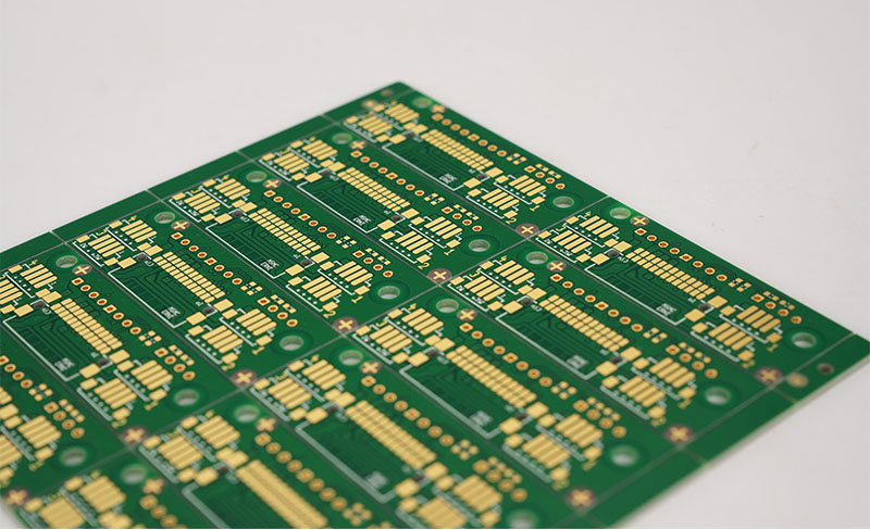
EBest Circuit reviewed the customer’s Gerber files, FR4 Tg130 requirement, 1.6 mm +/-10% board thickness, 1 oz copper, green solder mask, white silkscreen, lead-free HASL finish, and panel delivery requirement before production. The engineering team confirmed the free panelization arrangement, checked whether the panel format matched assembly preparation, and coordinated stencil support according to the customer’s next-step needs.

During fabrication, EBest Circuit controlled the key production steps for the 2L FR4 PCB, including material preparation, drilling, copper process, solder mask, silkscreen, lead-free HASL, routing, panel inspection, and final check. The boards were completed within the agreed 5-working-day PCB fabrication schedule after file confirmation. Before shipment, the team prepared the requested shipment report, dimension report, and COC.

Result

The European customer received the 2L FR4 rapid prototyping circuit boards in panel format, together with stencil support and the required shipment documents. This helped the customer move from prototype PCB fabrication to assembly preparation without waiting for extra documentation after delivery.
The case also shows why DFM support matters in rapid prototyping. The board itself was not highly complex, but the project still required correct panelization, delivery format, stencil preparation, and documentation. These details can affect the next build stage as much as the PCB fabrication process itself.

Why Choose EBest Circuit (Best Technology) for Rapid Prototyping Circuit Boards?

EBest Circuit (Best Technology) is suitable for rapid prototyping circuit boards when customers need engineering review, PCB fabrication, PCBA assembly, component sourcing, testing, and delivery support from one coordinated team. The company was founded in 2006 and supports customized PCB and PCBA solutions for global buyers.

The main reasons buyers choose EBest Circuit for rapid prototyping projects include:

  • Engineering-led support: one sales contact works with three engineers to support DFM review, BOM optimization, process questions, and production follow-up.
  • DFM pre-review before production: Gerber files, stack-up notes, material, panelization, surface finish, assembly preparation, and document requirements can be reviewed before the order enters production.
  • One-stop PCB and PCBA service: PCB fabrication, component sourcing, PCBA assembly, testing, and delivery follow-up can stay in one workflow.
  • Prototype and small-batch support: EBest Circuit supports samples and small batches, which is useful for R&D validation, assembly trials, and pilot build preparation.
  • Certified quality system: ISO 9001, ISO 13485, IATF 16949, AS9100D, REACH, RoHS, and UL-related quality support help customers meet industry and project requirements.
  • Traceable production: digital workshop tracking helps follow materials, product batches, production cycle, and production progress.
  • Fast PCBA delivery for suitable builds: for suitable PCBA projects, delivery can be about 1.5 weeks, depending on PCB complexity, component readiness, assembly difficulty, testing needs, and quantity.

For customers who need rapid prototyping circuit boards with DFM support, the value is not only fast board fabrication. The value is fewer open questions before production, clearer assembly preparation, and better documentation for the next build stage.

Send Gerber files, BOM, quantity, panelization notes, and testing requirements to sales@bestpcbs.com for an engineering review.

Rapid Prototyping Circuit Boards

FAQs about Rapid Prototyping Circuit Boards

What are rapid prototyping circuit boards?

Rapid prototyping circuit boards are early-stage PCB builds used to test and validate a PCB layout before pilot production or volume manufacturing. They help engineers check function, fit, manufacturability, assembly readiness, and documentation.

Why is DFM support important for rapid PCB prototypes?

DFM support helps identify manufacturing risks before production starts. It can catch spacing problems, drill issues, solder mask risks, panelization questions, missing notes, and assembly preparation problems that may delay the prototype build.

What files should I send for rapid prototyping circuit boards?

For PCB fabrication, send Gerber files, drill files, board thickness, copper thickness, material, surface finish, solder mask color, silkscreen color, quantity, and panelization requirements. For PCBA, also send BOM, pick-and-place files, assembly drawings, and test notes.

Can rapid prototyping circuit boards be delivered in panel format with stencil support?

Yes. Prototype PCBs can be delivered as individual boards or panels. If the boards will move into assembly, panel delivery and stencil support should be confirmed before production.

What documents can be provided with prototype PCB shipment?

Depending on the customer’s requirement, EBest Circuit can provide documents such as shipment report, dimension report, COC, test report, or other agreed production records.

Overall, rapid prototyping circuit boards are useful because they give engineers physical boards for layout validation, assembly preparation, and manufacturing review before a project moves into the next build stage.

For buyers who need DFM support, panelization, stencil support, shipment documentation, quick turn PCB boards fabrication, PCBA assembly, and traceable production follow-up, EBest Circuit (Best Technology) can review the files before production and help reduce avoidable questions during the prototype build. Pls feel free to send your Gerber files, BOM, quantity, and testing requirements to sales@bestpcbs.com for an engineering review.

You may also like

Top 10 High Quality PCB Manufacturing Companies in China

July 8th, 2026

High quality PCB manufacturing in China gives global buyers access to FR4 PCB, multi-layer PCB, metal core PCB, ceramic PCB, rigid-flex PCB, HDI PCB, high frequency PCB, component sourcing, and PCBA assembly through a concentrated supplier base. This guide compares 10 high quality PCB manufacturing companies in China and explains how engineers and sourcing teams can evaluate quality, capability, delivery, and supplier fit before placing an order.

EBest Circuit (Best Technology) is a high quality PCB manufacturer with its own PCB and PCBA factories, 20 years of PCB/PCBA experience, DFM pre-review, BOM optimization, one-stop PCB manufacturing and assembly, certified quality systems, and digital production traceability. If you are developing a custom electronics project and want a supplier to review your files before quotation, you can send Gerber files, BOM, stack-up requirements, quantity, and test needs to sales@bestpcbs.com for a practical engineering review.

high quality pcb manufacturing

Top 10 High Quality PCB Manufacturing Companies in China

The following list is written from a buyer’s perspective. It is not a financial ranking. The purpose is to help engineers and sourcing teams compare different types of PCB manufacturers in China, including large PCB groups, prototype-focused suppliers, multilayer PCB manufacturers, and one-stop PCB and PCBA partners.

1. EBest Circuit (Best Technology)

  • EBest Circuit (Best Technology) is a high quality PCB manufacturer in China, founded in 2006. The company provides customized PCB and PCBA solutions, including PCB prototype, mass production, component sourcing, PCB assembly, and turnkey electronics manufacturing service.
  • EBest is suitable for buyers who need engineering response, DFM review, BOM optimization, PCB fabrication, PCBA assembly, testing, and small-batch support from one coordinated team.
  • Best for: engineers and overseas buyers who need high quality PCB manufacturing, PCBA assembly, DFM support, and one-stop customized medical electronics manufacturing.

2. Kinwong

  • Kinwong is a listed PCB manufacturer in China with a broad product portfolio. Its public website lists conventional PCBs, flexible PCBs, metal base PCBs, rigid-flex PCBs, HDI PCBs, high layer count PCBs, RF PCBs, copper inlay, substrate-like PCB, and engineering design services.
  • Kinwong serves markets such as automotive, telecom, smart terminals, industrial and medical, consumer electronics, computing, and power supply. Buyers who need a large PCB manufacturer with broad technical coverage often include Kinwong in their comparison list.
  • Best for: large-scale buyers needing broad PCB technologies and established application coverage.

3. Suntak

  • Suntak is another well-known listed PCB manufacturer in China. Its public website shows product coverage such as high-layer boards, HDI, rigid-flex PCB, flex PCB, and IC substrate-related products. Suntak serves applications including mobile phones, servers, communication, automotive, computers, industrial control, medical, optoelectronics, and LED.
  • Suntak is relevant for buyers comparing suppliers for demanding products in communication, server, automotive, medical, and industrial fields.
  • Best for: multilayer PCB, HDI PCB, server, communication, automotive, and medical PCB applications.

4. Shennan Circuits

  • Shennan Circuits is widely recognized in China’s PCB industry and is often associated with advanced PCB manufacturing, communication electronics, data center hardware, automotive electronics, medical electronics, and industrial applications.
  • Because Shennan Circuits focuses on advanced manufacturing and larger customers, it may be more suitable for qualified projects with higher volume demand, strict approval requirements, and complex technical specifications.
  • Best for: larger projects requiring advanced PCB manufacturing and structured process systems.

5. Victory Giant Technology

  • Victory Giant Technology is a public PCB company based in Huizhou, Guangdong. It has received industry attention for advanced PCB production connected with AI, servers, graphics cards, and high-performance computing applications.
  • For buyers in fast-growing electronics fields, Victory Giant is often viewed as a manufacturer connected with complex and high-density PCB demand.
  • Best for: buyers researching high-end PCB suppliers for AI hardware, computing, server, or advanced electronics applications.

6. JLCPCB

  • JLCPCB is well known globally, especially among engineers, startups, makers, and small companies that need fast and accessible PCB prototyping. It provides online PCB ordering and also offers PCB assembly service.
  • JLCPCB can be a practical option for early-stage prototype validation, simple PCB fabrication, and projects that benefit from online quoting. For complex, high-reliability, or highly customized projects, buyers should still confirm material, testing, communication, and process-control requirements before production.
  • Best for: fast online PCB prototypes and low-volume engineering orders.

7. Fastprint

  • Fastprint, also known as Shenzhen Fastprint Circuit Tech, is known for prototype PCB, quick-turn PCB, and small-batch PCB manufacturing. It can be considered by customers who need faster engineering samples and early-stage production support.
  • As with any quick-turn PCB manufacturer, buyers should confirm whether the supplier can meet the required board structure, material, surface finish, tolerance, testing standard, and delivery schedule.
  • Best for: prototype PCB, quick-turn PCB, and small-batch PCB projects.

8. Ellington Electronics

  • Ellington Electronics Technology Group is a PCB manufacturer based in Zhongshan, Guangdong. It has been known for multilayer rigid PCBs and has served industries such as consumer electronics, telecommunications, computing, automotive, automation, power supply, and electronic test equipment.
  • Ellington can be considered when buyers need established PCB production experience and multilayer circuit board manufacturing.
  • Best for: buyers comparing established multilayer PCB manufacturers in South China.

9. WUS Printed Circuit

  • WUS Printed Circuit is a recognized PCB manufacturer with operations connected to communication, automotive, computing, and industrial electronics markets. It is often included when buyers research large PCB companies in China and Asia.
  • WUS may be more suitable for projects that require stable production planning, documented manufacturing systems, and structured supplier qualification.
  • Best for: communication, automotive, and industrial electronics PCB sourcing.

10. Founder PCB

  • Founder PCB is another PCB manufacturer often discussed in the Chinese PCB supply chain. It can be considered by buyers comparing production capacity, technical fit, quality requirements, and application coverage among multiple suppliers.
  • As with any PCB supplier, buyers should evaluate Founder PCB according to actual project needs, including board type, layer count, material, impedance control, testing, documentation, and communication efficiency.
  • Best for: buyers comparing multiple Chinese PCB manufacturers before supplier qualification.

What Makes a Company a High Quality PCB Manufacturer?

A high quality PCB manufacturer is not defined by one machine or one certificate. Quality comes from a complete manufacturing system. It includes engineering review, material control, process capability, inspection, testing, traceability, communication, and delivery reliability.

For engineering teams, a high quality PCB manufacturer should be able to support the project before production starts. This is where many problems can be prevented. A good supplier should review Gerber files, stack-up, material selection, copper thickness, line width, spacing, impedance requirements, drill and via structure, solder mask, surface finish, BOM risk, and assembly requirements before releasing the order to production.

Important evaluation factors include:

  • DFM review before PCB fabrication
  • BOM review and component risk checking before PCBA
  • Material and laminate options for FR4, high Tg, high speed, high frequency, ceramic, and metal core PCB
  • Stable copper plating and drilling control
  • Accurate line width and spacing control
  • Impedance control and reporting when required
  • AOI, electrical test, X-ray, functional test, and inspection support
  • Traceability from material to finished product
  • Quality certifications for regulated markets
  • Clear engineering communication and after-sales support

For high-reliability electronics, these details matter. A PCB can look correct visually but still fail because of weak via plating, uncontrolled impedance, poor solderability, incorrect material selection, inconsistent assembly, or insufficient testing. That is why buyers should choose a high quality PCB manufacturer that can explain the process clearly and respond to technical questions accurately.

How We Selected These High Quality PCB Manufacturers in China

This list was prepared for practical sourcing needs. We considered whether each company is relevant to buyers searching for high quality PCB manufacturing in China, and whether the company has visible PCB manufacturing capability, product coverage, market recognition, or application experience.

The selection factors include:

  • PCB manufacturing scope
  • Product range such as FR4 PCB, multilayer PCB, HDI PCB, rigid-flex PCB, flex PCB, RF PCB, ceramic PCB, and metal core PCB
  • Application fields such as automotive, medical, telecom, server, industrial, consumer electronics, and custom electronics
  • Suitability for prototypes, small batches, or larger production
  • Engineering support and production flexibility
  • Relevance to global sourcing and overseas buyer needs

The best supplier is not always the largest one. The best supplier is the one that matches your project stage, technical difficulty, order volume, delivery schedule, quality requirements, and communication needs.

Why Choose EBest Circuit (Best Technology) as Your High Quality PCB Manufacturer in China

EBest Circuit (Best Technology) is suitable for global buyers who need engineering review, process control, and clear production follow-up from the same supplier. Beyond bare PCB fabrication, it provides PCB manufacturing, PCBA assembly, component sourcing, testing, and project communication in one workflow.

A useful difference is the full-process service team. EBest Circuit can assign one business contact and three engineers to support the customer’s project, so technical questions about manufacturability, material selection, stack-up, component sourcing, assembly risks, testing, delivery, and documentation do not sit between separate departments.

The main reasons buyers choose EBest Circuit are:

  • Engineering-led support: one sales contact works with three engineers to provide DFM review, BOM optimization, and process suggestions before production.
  • One-stop PCB and PCBA service: PCB manufacturing, component sourcing, PCBA assembly, testing, and delivery follow-up are handled in one coordinated workflow.
  • Flexible for R&D projects: samples and small batches are supported, helping engineers reach prototype review or pilot build sooner.
  • Certified quality system: ISO 9001, ISO 13485, IATF 16949, AS9100D, REACH, RoHS, and UL-related quality support help customers meet industry requirements.
  • Traceable and reliable delivery: own PCB and PCBA factories, 1,000+ supply chain partners, digital workshop tracking, and fast PCBA delivery in about 1.5 weeks for suitable projects.

For overseas buyers, these advantages remove common handoff problems in custom PCB and PCBA projects. Instead of sending files to a supplier and waiting passively, customers can receive technical feedback, DFM suggestions, BOM optimization, production updates, and quality support from one coordinated team.

EBest Circuit High Quality PCB Manufacturing Capabilities for Global Buyers

EBest Circuit supports high quality PCB manufacturing for global buyers who need more than basic board production. Its capability is organized around a practical production task: turning released PCB files into boards that can be fabricated, assembled, tested, and documented.

1. Wide PCB structure capability

  • EBest Circuit supports standard 1-50 layer PCB production, with reviewed prototype capability up to 100 layers. This allows the company to support simple FR4 boards, multilayer PCBs, HDI-related projects, and complex electronic products.

2. Material options for different applications

  • EBest Circuit supports FR4 Tg130-140, Tg150, Tg170-180, high CTI, high speed, high frequency, ceramic-filled, PTFE, aluminum base, and copper base materials. This helps engineers choose suitable materials for signal speed, heat dissipation, insulation, cost, and reliability.

3. Thickness and copper control

  • The standard board thickness range is 0.4-6 mm, with reviewed prototype capability from 0.15-10 mm. For FR4 PCB, standard copper capability covers 0.5-6 oz inner copper and 0.5-10 oz outer copper, supporting both regular electronics and higher-current applications.

4. Fine circuit and surface finish support

  • For 1 oz outer copper, standard line/space capability can reach 3.5/4 mil. Surface finish options include lead-free HASL, ENIG, immersion tin, immersion silver, OSP, hard gold, soft gold, ENIG + OSP, ENEPIG, and plated gold finger.

5. Impedance-controlled PCB manufacturing

  • For impedance-controlled PCB, EBest Circuit can support standard impedance tolerance of +/-5 ohms below 50 ohms and +/-10% at or above 50 ohms. Impedance reports can be provided when required for engineering validation.

6. From PCB fabrication to PCBA assembly

  • EBest Circuit integrates PCB manufacturing, component sourcing, PCBA assembly, testing, and delivery follow-up in one service flow. This reduces communication gaps between separate suppliers and shortens the handoff from released PCB layout files to production.

Behind these capabilities, EBest Circuit provides DFM pre-review, BOM optimization, process adaptation suggestions, and digital workshop tracking for materials, product batches, production cycle, and production progress. For global buyers, this means the factory is not only making boards, but also helping control manufacturing risk before and during production.

High Quality PCB Fabrication and Assembly Services EBest Circuit Provides

Many global buyers prefer one supplier that can provide both PCB fabrication and PCB assembly. This reduces communication gaps between the bare board factory, component sourcing team, and assembly factory. It also helps solve DFM, DFA, BOM, soldering, inspection, and testing issues earlier.

EBest Circuit provides one-stop PCB and PCBA service, including:

  • PCB layout support
  • PCB prototype
  • PCB fabrication
  • Mass production
  • Component sourcing
  • BOM optimization
  • SMT assembly
  • Through-hole assembly
  • Mixed assembly
  • PCBA testing
  • Box build or system integration support when required

The company can support Metal Core PCB, Ceramic PCB, FR4 PCB, Special PCB, PCB layout, PCB Prototype, Mass Production, Component Sourcing, and PCB Assembly. Its product lines also include MCPCB, ceramic PCB, rigid-flex circuits, FR4 PCB, heavy copper PCB, HDI PCB, high Tg PCB, RF PCB, multilayer PCB, and special PCB.

For engineers developing custom electronics, this service model reduces supplier coordination work. The same team can review PCB files, assembly files, component risks, process adaptation, and final test requirements.

How EBest Circuit Controls Quality and Reliability in PCB and PCBA Manufacturing

High quality PCB manufacturing depends on quality control before, during, and after production. EBest Circuit supports this through engineering review, manufacturing process capability, certified quality systems, digital traceability, and inspection control.

The company holds or supports quality-related certifications and compliance systems including:

  • ISO 9001:2015
  • ISO 13485:2016
  • IATF 16949
  • AS9100D
  • REACH
  • RoHS
  • UL

These certifications are important for customers in automotive electronics, medical devices, aerospace-related products, industrial equipment, and other regulated or reliability-sensitive markets.

Quality control can include:

  • DFM pre-review before PCB production
  • BOM optimization before PCBA assembly
  • Material verification
  • Process control for drilling, plating, imaging, etching, solder mask, and surface finish
  • AOI inspection
  • Electrical test
  • Impedance test and impedance report when required
  • Solder paste and placement checks for PCBA
  • X-ray inspection for BGA or hidden solder joints when required
  • Functional testing according to customer requirements
  • Final inspection before shipment
  • Digital tracking for materials, batches, production cycle, and production progress

The digital workshop is especially useful for overseas customers because it improves visibility. EBest Circuit can track materials and product batches, production cycle, and production progress within 5 seconds. This helps customers understand where the order is, what stage it is in, and how production is moving.

Case Study: High Quality PCB Manufacturing for a 4L FR4 Impedance Control PCB

This case shows how EBest Circuit supports a custom PCB project that requires controlled impedance and an impedance report.

Project requirement

The customer needed a 4-layer PCB for a custom electronics application. The technical requirements included:

  • Board type: 4L PCB
  • Material: FR4 Tg130
  • Outer copper thickness: 1 oz
  • Inner copper thickness: 0.5 oz
  • Finished board thickness: 1.53 mm +/-10%
  • Solder mask and silkscreen: blue solder mask with white silkscreen
  • Surface finish: ENIG
  • Impedance requirement: 50 ohm single-ended impedance
  • Controlled trace: 18.653 mil trace width on the top layer
  • Documentation: impedance report required

Customer challenge

  • The key challenge was not only producing a standard 4-layer FR4 PCB. The customer needed stable impedance control on the top layer and required a formal impedance report. For this type of project, small changes in copper thickness, dielectric thickness, stack-up, trace width, solder mask, and finished board thickness can affect final impedance performance.
  • If the PCB manufacturer does not review the stack-up and controlled trace carefully before production, the customer may receive boards that pass visual inspection but fail signal performance requirements.

EBest Circuit solution

  • EBest Circuit reviewed the customer’s released PCB layout files and confirmed the critical manufacturing parameters before production. The engineering team checked the FR4 Tg130 material, 4-layer stack-up, 1 oz outer copper, 0.5 oz inner copper, 1.53 mm +/-10% finished thickness, ENIG surface finish, and top-layer impedance trace requirement.
  • Because the customer required 50 ohm single-ended impedance, the team controlled the 18.653 mil top-layer trace width according to the agreed stack-up and manufacturing process. The project was also aligned with the company’s impedance tolerance capability, which supports standard impedance control of +/-5 ohms for values below 50 ohms and +/-10% for values at or above 50 ohms.
  • During production, EBest Circuit controlled key process steps such as material selection, lamination, copper thickness, imaging, etching, solder mask, ENIG surface finish, and final inspection. After production, the impedance requirement was verified and an impedance report was provided to the customer.

Result

  • The customer received a 4-layer FR4 PCB that matched the required material, copper thickness, board thickness, blue solder mask, white silkscreen, ENIG finish, and 50 ohm single-ended impedance control requirement. The impedance report gave the customer the documentation needed for engineering validation and project records.

This case reflects why working with a high quality PCB manufacturer is important. For impedance-controlled products, the supplier must understand both the layout requirement and the manufacturing variables that affect electrical performance.

When to Choose an OEM PCB Manufacturer for High Quality Electronics

An OEM PCB manufacturer for high quality electronics is most useful when a project goes beyond bare board production. Typical requirements include custom PCB fabrication, component sourcing, PCBA assembly, testing, and long-term supply chain cooperation.

EBest Circuit is suitable for OEM and custom electronics projects in these situations:

  • Prototype, sample, or small-batch orders need engineering follow-up.
  • The PCB layout is ready, but manufacturability still needs to be checked before production.
  • BOM risk, component sourcing, and assembly preparation need to be handled together.
  • PCB manufacturing and PCBA assembly should stay with one supplier to reduce handoff risk.
  • The project involves impedance control, special material, heavy copper, HDI, metal core, ceramic, or high frequency PCB.
  • The end market requires quality certifications, traceable production progress, batch records, or faster PCBA delivery for suitable builds.

For engineers, the benefit is shorter validation cycles without separating PCB fabrication, sourcing, and assembly work. EBest Circuit can support samples and small batches, helping engineering teams verify the PCB layout and prepare it for pilot production. For suitable PCBA projects, fast delivery in about 1.5 weeks can help reduce development waiting time.

high quality pcb manufacturing

FAQs About High Quality PCB Manufacturing

What is high quality PCB manufacturing?

High quality PCB manufacturing means producing printed circuit boards with stable material selection, accurate dimensions, reliable copper plating, controlled line width and spacing, consistent solder mask, proper surface finish, complete testing, and traceable production control. It also includes engineering support before production.

Why is EBest Circuit a high quality PCB manufacturer?

EBest Circuit combines PCB manufacturing, PCBA assembly, component sourcing, DFM review, BOM optimization, quality certifications, digital workshop traceability, and engineering support. Its service model includes one business contact and three engineers supporting the full project flow.

What PCB types can EBest Circuit manufacture?

EBest Circuit can support FR4 PCB, multilayer PCB, metal core PCB, ceramic PCB, flexible PCB, rigid-flex PCB, high frequency PCB, HDI PCB, heavy copper PCB, high Tg PCB, RF PCB, and special PCB.

Can EBest Circuit provide PCB assembly?

Yes. EBest Circuit provides one-stop PCB and PCBA service, including PCB fabrication, component sourcing, SMT assembly, through-hole assembly, mixed assembly, testing, and related turnkey support.

Can EBest Circuit support impedance controlled PCB?

Yes. EBest Circuit can support impedance controlled PCB and provide impedance reports when required. Its process capability table lists standard impedance tolerance of +/-5 ohms below 50 ohms and +/-10% at or above 50 ohms.

What certifications does EBest Circuit have?

EBest Circuit’s quality certifications and compliance support include ISO 9001:2015, ISO 13485:2016, IATF 16949, AS9100D, REACH, RoHS, and UL.

Can EBest Circuit support sample and small-batch PCB production?

Yes. EBest Circuit supports samples and small batches, helping engineers complete PCB layout validation and reach the next build stage sooner.

How fast can EBest Circuit deliver PCBA?

For suitable projects, EBest Circuit can support fast PCBA delivery in about 1.5 weeks. Actual delivery time depends on PCB complexity, component availability, assembly difficulty, testing requirements, and order quantity.

What files should I send for a PCB or PCBA quotation?

For PCB manufacturing, send Gerber files, drill files, stack-up requirements, material requirements, copper thickness, board thickness, surface finish, impedance requirements, and quantity. For PCBA, also send BOM, pick-and-place file, assembly drawings, test requirements, and special acceptance standards.

All in all, choosing a high quality PCB manufacturing company in China is not only about finding the lowest price; the right supplier should help you control engineering risk, manufacturing quality, delivery time, component sourcing, assembly quality, and long-term reliability.

Large manufacturers such as Kinwong, Suntak, Shennan Circuits, Victory Giant, JLCPCB, Fastprint, Ellington, WUS, and Founder PCB all serve different PCB market needs, while EBest Circuit (Best Technology) is worth shortlisting if you need responsive engineering support, DFM review, BOM optimization, PCB manufacturing, component sourcing, PCBA assembly, testing, and traceable production. A warm welcome to send your Gerber files, BOM, quantity, and testing requirements to sales@bestpcbs.com for an engineering review.

You may also like

Double Sided PCB Boards Manufacturer | 2 Layer PCB Prototype & Production

July 8th, 2026

Double sided PCB boards are among the most widely used circuit board structures in electronics manufacturing. They provide conductive copper layers on both sides of an insulating substrate, allowing engineers to route more signals, place more components, and build more compact products than with a single sided PCB.

For many engineering teams, a double sided PCB board is the practical starting point for product development. It is simpler and more cost-effective than a multilayer PCB, but it gives much more routing flexibility than a one-layer board. That is why double sided printed circuit boards are commonly used in control modules, sensor boards, power interfaces, LED products, communication devices, industrial electronics, and prototype-to-production PCBA projects.

This guide explains how double sided PCB boards work, how they are manufactured, how to choose materials and surface finishes, and what to check before ordering a double sided PCB board prototype or custom production run.

Double sided PCB boards for 2 layer PCB prototype and production

What Are Double Sided PCB Boards?

Double sided PCB boards are printed circuit boards with copper circuitry on both the top and bottom sides of the board. The two copper layers are separated by an insulating base material, usually FR4, and connected through vias or plated through holes.

In a basic single sided PCB, all routing must stay on one copper layer. This limits circuit density and can make layouts larger or less efficient. In double sided PCB boards, traces can move from one side to the other through vias. This allows signals, power, and ground paths to be arranged more efficiently.

In practical terms, double sided PCB boards are often called 2 layer PCBs. The two terms are closely related in most manufacturing and quoting situations:

TermCommon Meaning
Double sided PCB boardA PCB with copper circuits on both sides
2 layer PCBA PCB with two conductive copper layers
Double sided printed circuit boardA formal name for the same PCB structure
Double sided copper clad PCB boardThe copper-clad board structure before or during fabrication

For engineers, the value is clear: a double sided PCB board can support denser routing, better component placement, more stable ground paths, and a more compact final assembly.

Double Sided PCB Board vs Single Sided and Multilayer PCBs

A double sided PCB board sits between a simple single sided PCB and a more complex multilayer PCB. Choosing the right structure depends on circuit complexity, product size, signal requirements, budget, and production volume.

PCB TypeStructureBest ForMain Limitation
Single sided PCBCopper on one sideSimple circuits, low-cost productsLimited routing space
Double sided PCB boardCopper on both sidesPrototypes, control boards, compact electronicsLess routing freedom than multilayer PCBs
Multilayer PCBThree or more copper layersHigh-density, high-speed, impedance-controlled productsHigher cost and longer engineering review

Single sided boards are suitable when the circuit is simple and the size is not restricted. Multilayer PCBs are better when the product needs high-speed signals, controlled impedance, complex BGA routing, or dedicated power and ground planes.

Double sided PCB boards are often the best choice when the project needs a balance between cost, routing flexibility, and manufacturability. They are especially useful in early product development because engineers can verify the circuit, test the layout, and move to small-batch production without immediately paying for a multilayer stackup.

Single sided PCB, double sided PCB board, and multilayer PCB structure comparison

Double Sided Copper Clad PCB Board Structure

A double sided copper clad PCB board starts with a dielectric core material laminated with copper foil on both sides. After imaging, etching, drilling, plating, solder mask, surface finishing, and testing, it becomes a finished double sided PCB board.

A typical structure includes:

  • Base material, such as FR4
  • Copper foil on the top side
  • Copper foil on the bottom side
  • Drilled holes and vias
  • Plated through holes for layer-to-layer connection
  • Solder mask to protect copper circuits
  • Silkscreen for component marks and assembly labels
  • Surface finish such as ENIG, HASL, OSP, or immersion silver

The key difference between a copper clad board and a finished PCB is processing. The copper clad laminate is the raw board material. A finished double sided PCB board has defined circuit patterns, holes, plated copper, solder mask, surface finish, and electrical testing.

For a custom double sided PCB board, engineers should pay attention to copper thickness, finished board thickness, minimum trace and spacing, minimum hole size, annular ring, solder mask bridge, and surface finish requirements. These details affect both cost and production yield.

Materials for Double Sided Printed Circuit Boards

Most double sided printed circuit boards use FR4 because it offers a practical balance of insulation, mechanical strength, cost, and availability. FR4 is suitable for many consumer electronics, industrial controls, power interfaces, test fixtures, and general electronic assemblies.

Common material and build options include:

ItemCommon OptionsWhy It Matters
Base materialFR4, high Tg FR4, aluminum, ceramic, flexible materialDetermines thermal, mechanical, and electrical performance
Copper thickness0.5oz, 1oz, 2oz, or heavier copper when requiredAffects current carrying capacity and trace width
Board thicknessThin boards, standard 1.6mm boards, or thicker boardsAffects rigidity, assembly, enclosure fit, and mechanical strength
Solder maskGreen, white, black, blue, red, and other colorsProtects copper and supports inspection/branding
Surface finishENIG, HASL, lead-free HASL, OSP, immersion silverAffects solderability, shelf life, flatness, and assembly reliability

For SMT assembly, ENIG is often selected when the board needs a flat surface finish, good solderability, or fine-pitch component support. HASL may be suitable for cost-sensitive products with less demanding surface flatness requirements. OSP can also be used in many SMT projects, but storage and handling should be controlled carefully.

When selecting materials for double sided PCB boards, the best choice is not always the most expensive one. The right material depends on current load, operating temperature, product environment, assembly method, and expected product life.

How Double Sided PCB Boards Are Made

At EBest Circuit, a double sided PCB board order does not start directly from fabrication. It starts with engineering review. Before the board enters production, our team checks the Gerber files, drill data, stackup requirements, copper weight, board thickness, surface finish, solder mask, silkscreen, panelization notes, and any PCBA assembly files if SMT is required.

The following is a real 2 layer PCB process example from an EBest Circuit production traveler. In this case, the board used S1141 material, Tg 140, 0.865mm base thickness, H/H copper foil, and a working panel size of 260.25 x 415.00mm. The process route shows how a double sided PCB board moves from raw laminate to final shipment.

Process StepControl Point
Material cuttingMaterial, Tg, base thickness, copper foil, and panel size
DrillingDrill file and minimum hole size, such as 0.95mm in this example
Electroless copper and panel platingHole copper and surface copper, such as 20um and 35um
Outer layer imagingDry film, polarity, trace width, spacing, and pad clearance
Outer layer inspectionCircuit pattern before plating and etching
Pattern tin platingTin plating on required circuit areas
EtchingTrace width, spacing, pad clearance, and line tolerance
Etching inspectionVisual check after circuit formation
Solder maskSolder mask opening, color, and double-sided application
BakingMoisture and process stability before finishing
Lead-free HASLLead-free surface finish and tin thickness, such as 1-40um
Flying probe testElectrical opens and shorts
ProfilingBoard outline and tolerance, such as +/-0.13mm
Final inspectionThickness, tolerance, warpage, and IPC-A-600 standard
PackingVacuum packing, QA report, test report, samples, and humidity card

For double sided PCB boards, drilling, copper deposition, plating, etching, solder mask, surface finish, and electrical testing are especially important. Vias and plated through holes create the electrical connection between the top and bottom copper layers. If the hole wall plating is weak, the board may pass visual inspection but fail during electrical testing, assembly, or long-term operation.

This is why EBest Circuit places DFM review before production. Our engineering team checks whether the customer’s layout is suitable for the selected process. Common review points include minimum trace and spacing, annular ring, hole size, copper-to-edge clearance, solder mask bridge, surface finish selection, finished board thickness, outline tolerance, and whether the board structure matches the assembly method.

For PCBA projects, the review also extends to BOM, component footprint, polarity, silkscreen direction, pick-and-place data, and assembly notes. This helps engineers avoid a common problem: the PCB can be fabricated, but the assembly becomes difficult or risky.

Double Sided PCB Board Prototype Cost and Lead Time

A double sided PCB board prototype is used to verify electrical function, mechanical fit, assembly feasibility, and production risk before larger-volume manufacturing. From EBest Circuit’s point of view, prototype cost and lead time are not decided by board size alone. They are decided by the full technical package.

When our team reviews a double sided PCB board prototype, we usually look at:

  • Board size and panel utilization
  • Board thickness
  • Copper thickness
  • Minimum trace and spacing
  • Minimum drill size
  • Surface finish
  • Solder mask and silkscreen color
  • Quantity
  • Electrical test requirements
  • SMT assembly requirements
  • Component sourcing method

For example, one practical EBest Circuit 2L PCB project used FR4 Tg130, 1oz copper, 0.25mm board thickness, ENIG surface finish, white solder mask, and black silkscreen. The project also required SMT assembly, with components supplied by the customer.

For this type of project, the work is not only “make the bare PCB.” It becomes a coordinated PCBA prototype. The manufacturer must manage PCB fabrication, incoming material check, solder paste printing, SMT placement, reflow soldering, inspection, and final assembly review.

This is why EBest Circuit does not quote prototype timing only from the layer count. A simple bare double sided PCB board may move quickly, but a PCBA prototype also depends on component readiness, stencil preparation, assembly complexity, inspection requirements, and test scope.

For engineers, the most useful way to shorten lead time is to prepare a complete file package at the beginning: Gerber files, drill files, BOM, pick-and-place files, assembly drawing, polarity notes, and any special testing requirements. With complete files and available materials, EBest Circuit can support fast sample and small-batch PCBA delivery, with urgent PCBA projects reaching about 1.5 weeks in suitable conditions.

How to Use Double Sided PCB Board in Real Projects

Engineers use double sided PCB boards when a product needs more routing freedom than a single sided board but does not yet require a multilayer stackup. This makes them useful in many real development and production situations.

Common use cases include:

  • Sensor control boards
  • LED control modules
  • Power interface boards
  • Communication accessories
  • Industrial control boards
  • Consumer electronic modules
  • Test fixtures
  • Small embedded system boards
  • Prototype boards for functional verification

In one EBest Circuit project, the customer needed a compact 2 layer PCB with SMT assembly. The board used FR4 Tg130, 1oz copper, 0.25mm finished thickness, ENIG surface finish, white solder mask, and black silkscreen. The customer supplied the components, while EBest Circuit supported PCB fabrication and SMT assembly.

This is a good example of how double sided PCB boards are used in real product development. The board was thin, so mechanical handling and assembly support had to be considered. ENIG was selected to provide a flat soldering surface for SMT. The white solder mask and black silkscreen helped with visual identification, assembly marks, and product appearance.

In this type of 2 layer PCB layout, the top layer may carry key components and signals, while the bottom layer may support additional routing, ground return paths, and connector placement. With proper via planning, the layout can stay compact without moving immediately to a 4 layer PCB.

For PCBA projects, a double sided PCB board may also support components on one side or both sides. If components are placed on both sides, the assembly process must consider soldering sequence, component weight, reflow profile, inspection access, and whether any parts require hand soldering or selective soldering.

This is where practical engineering support matters. A manufacturer that understands both PCB fabrication and PCB assembly can help identify layout and assembly risks before production, not after boards are already made. At EBest Circuit, one business contact works together with three engineering support roles to respond to engineering needs across DFM review, BOM optimization, PCB manufacturing, SMT assembly, and testing.

Custom Double Sided PCB Board Layout Guidelines

A custom double sided PCB board should be designed with manufacturing and assembly in mind. Here, layout does not mean full circuit design or schematic development. It means the practical PCB layout and DFM decisions that help the board move smoothly into fabrication and assembly.

Important layout guidelines include:

  • Keep trace width and spacing within the manufacturer capability.
  • Use proper annular ring around vias and plated holes.
  • Avoid placing vias too close to pads unless via-in-pad is intentionally specified.
  • Maintain sufficient solder mask bridge between fine-pitch pads.
  • Keep copper balance reasonable on both sides of the board.
  • Use clear polarity and orientation marks for SMT assembly.
  • Confirm connector placement and mechanical clearance.
  • Provide complete Gerber, drill, BOM, pick-and-place, and assembly files for PCBA.
  • Use test points where functional testing is required.
  • Review panelization requirements before production.

For 1oz copper double sided PCB boards, trace width and spacing should be selected based on current, voltage, impedance needs, and the factory’s production capability. A layout that looks correct on screen may still create fabrication risk if it pushes minimum spacing, drill, or solder mask limits too aggressively.

EBest Circuit provides DFM analysis and process adaptation suggestions through an engineering support team with long-term PCB and PCBA experience. For engineers, this helps reduce repeated revisions, avoid unclear fabrication notes, and improve the chance of successful first-run production.

When to Choose a Double Sided Flexible PCB Board

A double sided flexible PCB board is different from a standard rigid FR4 double sided PCB board. It uses flexible base material and is designed for products that require bending, folding, or space-saving interconnection.

Double sided flexible PCB boards may be suitable for:

  • Wearable electronics
  • Compact medical devices
  • Display modules
  • Camera modules
  • Sensor connections
  • Foldable or moving electronic assemblies
  • Space-limited product designs

However, flexible PCBs require different design and manufacturing rules. Bend radius, coverlay openings, stiffener placement, copper type, dynamic bending requirements, and connector reinforcement all need attention. A layout that works on rigid FR4 may not be suitable for a flexible circuit.

If the product only needs a compact but rigid assembly, a standard double sided PCB board may be more cost-effective. If the product needs repeated bending or tight mechanical integration, a double sided flexible PCB board or rigid-flex PCB may be the better option.

Why Work with a Double Sided PCB Boards Manufacturer with PCBA Support

Choosing a double sided PCB boards manufacturer is not only about bare board price. For engineering teams, the real value often comes from file review, manufacturability feedback, component support, assembly control, testing, traceability, and delivery management.

EBest Circuit (Best Technology), founded in 2006, provides customized PCB and PCBA solutions for global customers. The service scope includes FR4 PCB, metal core PCB, ceramic PCB, special PCB, PCB prototype, mass production, component sourcing, and PCB assembly.

For double sided PCB boards and 2 layer PCB projects, the company can support:

  • PCB fabrication
  • Component sourcing
  • Customer-supplied component assembly
  • SMT assembly
  • PCBA testing
  • Prototype and small-batch production
  • DFM pre-review
  • BOM optimization suggestions
  • Engineering process adaptation advice

The company operates its own PCB and PCBA factory, works with more than 1,000 supply chain partners, and has served more than 10,000 engineers and over 1,800 customers. Its quality system includes ISO 9001, ISO 13485, IATF 16949, AS9100D, REACH, RoHS, and UL-related compliance support.

For production traceability, a digital workshop can track materials, product batches, production cycle, and production progress quickly. This helps engineering teams manage quality, schedule, and repeat orders more clearly.

The best result comes when engineers and manufacturers work together early. If the PCB manufacturer reviews the Gerber files, BOM, assembly notes, and process requirements before fabrication, the project has a better chance of moving from prototype to production without costly delays.

FAQs about Double Sided PCB Boards

What are double sided PCB boards?

Double sided PCB boards are printed circuit boards with copper circuits on both the top and bottom sides. The two layers are connected by vias or plated through holes, allowing more compact and flexible routing than a single sided PCB.

Is a double sided PCB board the same as a 2 layer PCB?

In most manufacturing and quoting contexts, yes. A double sided PCB board usually means a 2 layer PCB with one copper layer on each side of the board.

What is a double sided copper clad PCB board?

A double sided copper clad PCB board is the base board material with copper foil laminated on both sides. After imaging, etching, drilling, plating, solder mask, surface finish, and testing, it becomes a finished double sided PCB board.

When should I use a double sided PCB board?

Use a double sided PCB board when a single sided board cannot provide enough routing space, but the project does not need the cost or complexity of a multilayer PCB. It is a practical choice for many prototypes, control boards, and compact electronic products.

What affects double sided PCB board prototype cost?

Prototype cost depends on board size, thickness, copper weight, surface finish, trace and spacing requirements, drill size, quantity, electrical testing, and whether SMT assembly or component sourcing is required.

Can double sided PCB boards support SMT assembly?

Yes. Double sided PCB boards are widely used for SMT assembly. For PCBA projects, engineers should provide Gerber files, BOM, pick-and-place files, assembly drawings, and any special testing requirements.

What files are needed for a custom double sided PCB board?

Most projects require Gerber files, drill files, board specifications, solder mask and silkscreen requirements, and surface finish selection. PCBA projects also require BOM, pick-and-place files, assembly notes, and test requirements.

What is the difference between a double sided PCB board and a double sided flexible PCB board?

A standard double sided PCB board is usually rigid, often made from FR4. A double sided flexible PCB board uses flexible material and is designed for bending, folding, or compact interconnection in space-limited products.

How can DFM review help double sided PCB boards?

DFM review checks whether the board can be manufactured reliably. It can identify risks such as insufficient spacing, small annular rings, unclear drill data, solder mask issues, panelization problems, and assembly mismatches before production starts.

How do I choose a double sided PCB boards manufacturer?

Choose a manufacturer that can support PCB fabrication, engineering review, material selection, SMT assembly, testing, quality control, and delivery management. For prototype and PCBA projects, one-stop support can reduce communication gaps and production risk.

Ready to Build Your Double Sided PCB Boards?

If you are working on a double sided PCB board prototype, a 2 layer PCB layout, or a PCBA project that needs fabrication, components, SMT assembly, and testing, you do not have to solve every production detail alone.

Send your Gerber files, BOM, pick-and-place file, drawings, or even early project questions to EBest Circuit. Our team will review the details carefully and help you find a practical way forward.

Email us at sales@bestpcbs.com. Tell us what you are building, what stage you are in, and what worries you most. We will help you turn the board from a file on your screen into a working product in your hands.

You may also like

Top 10 Largest Printed Circuit Board Manufacturers in China

July 7th, 2026

Largest printed circuit board manufacturers in China are PCB companies with strong production scale, advanced process capability, stable quality systems, and broad customer coverage. This article explains how large PCB manufacturers are ranked, lists 10 major PCB companies in China, and shows how buyers can choose between large-volume PCB makers and custom PCB manufacturers.

Why do buyers search for the largest printed circuit board manufacturers before sending an RFQ?

  • They do not know which PCB company is truly reliable.
  • They worry that small suppliers cannot handle complex PCB requirements.
  • They see many “top PCB manufacturers” lists but no clear comparison logic.
  • They are unsure whether a large PCB factory accepts prototype or custom projects.
  • They need proof: certifications, capacity, PCB types, PCBA support, and overseas service.

A better supplier selection process should connect company size with real project fit.

  • Check ranking factors, not only company names.
  • Compare PCB types, process limits, certifications, and lead time.
  • Decide whether the project needs high-volume production or flexible customization.
  • Review PCBA, component sourcing, and testing capability when needed.
  • Choose a PCB manufacturer that matches the product stage and technical risk.

EBest Circuit (Best Technology) is a China-based PCB and PCBA manufacturer supporting custom PCB fabrication, PCB prototype, mass production, component sourcing, PCB assembly, and turnkey PCB solutions. Our capabilities cover FR4 PCB, Metal Core PCB, Ceramic PCB, HDI PCB, flexible PCB, rigid-flex PCB, high-frequency PCB, heavy copper PCB, and PCBA. For project review or quotation, contact sales@bestpcbs.com.

Largest Printed Circuit Board Manufacturers

What Does “Largest Printed Circuit Board Manufacturers” Mean?

The largest printed circuit board manufacturers are usually judged by revenue, production capacity, customer base, factory scale, technical capability, and global supply coverage. However, “largest” does not always mean “best for every project.”

A company may be very large because it serves smartphone, server, automotive, telecom, or AI hardware programs. That does not automatically mean it is the best choice for a small-batch ceramic PCB, an urgent prototype, or a custom PCBA order.

Ranking FactorWhy It Matters
RevenueMarket scale
CapacityVolume support
PCB TypesTechnical range
CertificationsQuality proof
CustomersIndustry trust
Overseas SupportExport readiness

The global PCB market is large and still growing. ResearchAndMarkets estimated the PCB market at $67.9 billion in 2023 and projected it to reach $92.4 billion by 2029, which explains why buyers pay close attention to major PCB manufacturing regions and large suppliers.

For buyers, the practical meaning is simple: use “largest” as a starting point, not the final decision.

Largest Printed Circuit Board Manufacturers

How Are the Largest PCB Manufacturers in China Ranked?

The largest PCB manufacturers in China can be ranked in different ways. Some lists focus on revenue. Others focus on output, factory area, domestic ranking, global ranking, or a specific product category such as HDI PCB, FPC, IC substrate, server PCB, or automotive PCB.

A clean ranking method should include:

  • Business scale: revenue, capacity, and customer base.
  • Product capability: multilayer PCB, HDI PCB, FPC, rigid-flex PCB, heavy copper PCB, high-frequency PCB.
  • Quality system: ISO, IATF, AS9100, UL, RoHS, REACH, or medical-related systems.
  • Industry coverage: automotive, communication, data center, medical, industrial, consumer electronics.
  • Engineering support: DFM, stack-up review, impedance control, PCBA, testing, and overseas service.

This is why PCB manufacturer ranking should not be read like a simple winner list. A high-volume factory may be excellent for server boards but less flexible for small custom projects. A custom PCB manufacturer may not be the largest, but it may provide better engineering response, MOQ flexibility, and special-board support.

Top 10 Largest Printed Circuit Board Manufacturers in China

The following list is a practical B2B reference of large and well-known printed circuit board manufacturers in China. The order may vary by year, revenue source, and ranking method, so buyers should use it as a supplier research starting point rather than a fixed audited ranking.

CompanyStrong AreaBest Fit
Shennan CircuitsPCB + IC substrateHigh-reliability electronics
Dongshan Precision / MultekPCB, FPC, rigid-flexHigh-density projects
Victory Giant TechnologyAI server PCBHigh-speed, high-volume
KinwongMultilayer PCBGlobal PCB supply
WUS Printed CircuitServer, AI, automotiveHPC and data center
Suntak TechnologyMultilayer, HDILarge-volume PCB
Aoshikang TechnologyHigh-precision PCBServer, auto, telecom
Fastprint Circuit TechPrototype, small batchEngineering projects
Founder PCBMultilayer, HDICommunication, smart devices
Guangdong EllingtonDouble-sided, multilayerHigh-density PCB
  • Shennan Circuits: Its core business covers printed circuit boards, packaging substrates, and electronic assembly, making it one of China’s more technology-driven PCB companies.
  • Dongshan Precision / Multek: Multek supports rigid PCB, FPC/FPCA, PCB, and rigid-flex products. Its rigid PCB capability includes high-layer-count and HDI structures.
  • Victory Giant Technology: Victory Giant is recognized as a major Chinese PCB manufacturer and is strongly associated with AI server and high-performance computing PCB demand.
  • Kinwong: Kinwong reported 2024 annual revenue of $1.762 billion and describes itself as one of the world’s largest printed circuit board suppliers.
  • WUS Printed Circuit: WUS manufactures PCBs for high-speed servers, accelerator modules, automotive domain controllers, AI, HPC, autonomous driving, medical, industrial, and navigation applications.
  • Suntak Technology: Suntak reports large annual capacity and positions itself as a listed high-tech company producing circuit boards for communications, servers, computers, medical electronics, industrial HDI, automotive electronics, mobile phones, and optoelectronics.
  • Aoshikang Technology: Aoshikang focuses on R&D, production, and sales of high-precision PCBs used in data centers, servers, automotive electronics, communications, and consumer electronics.
  • Fastprint Circuit Tech: Fastprint is headquartered in Shenzhen, listed on the Shenzhen Stock Exchange, and operates manufacturing campuses in Guangzhou, Yixing, and the UK.
  • Founder PCB: Founder PCB is a PCB company headquartered in Zhuhai, Guangdong, with a long operating history in multilayer and HDI PCB manufacturing.
  • Guangdong Ellington: Guangdong Ellington focuses on high-precision, high-density double-sided and multilayer printed circuit boards.
Largest Printed Circuit Board Manufacturers

Why Are Many of the Largest PCB Manufacturers Based in China?

Many of the largest PCB manufacturers are based in China because China has a complete electronics manufacturing ecosystem. PCB production depends on copper foil, laminate, drilling, plating, imaging, solder mask, surface finish, SMT, components, testing, packaging, and export logistics. China has dense supply-chain support for each step.

China’s PCB manufacturing advantage usually comes from:

  • Strong electronics supply chains in the Pearl River Delta and Yangtze River Delta.
  • Large demand from communication, automotive, consumer electronics, AI servers, and industrial equipment.
  • Mature support for PCB materials, surface treatment, mechanical processing, and assembly.
  • Wide factory choices, from high-volume PCB manufacturers to custom PCB manufacturers.
  • Strong export experience for overseas electronics companies.

For buyers, this means China is not only a low-cost PCB sourcing region. It is also a technical manufacturing hub with large printed circuit board manufacturers, prototype PCB manufacturers, PCBA service providers, and special PCB factories.

Large PCB Manufacturers vs Custom PCB Manufacturers in China

Large PCB manufacturers and custom PCB manufacturers serve different needs. The largest printed circuit board manufacturers in China are often strong in scale, automation, large customers, and stable high-volume production. Custom PCB manufacturers are often more flexible in special boards, engineering support, prototype orders, and communication.

Supplier TypeBest ForPossible Limitation
Large PCB manufacturersHigh-volume productionLess flexible MOQ
Custom PCB manufacturersSpecial PCB projectsSmaller scale
Prototype PCB manufacturersFast engineering samplesLimited mass volume
PCBA manufacturersFinished assembliesNeeds BOM clarity

A large factory is a good choice when the project has stable design files, large demand, and clear process requirements. A custom printed circuit board manufacturer is often better when the project needs HDI PCB, ceramic PCB, Metal Core PCB, heavy copper PCB, rigid-flex PCB, impedance control, unusual thickness, special materials, or PCBA support.

The right question is not “Which PCB manufacturer is the largest?” The better question is: “Which manufacturer fits this product?”

What PCB Types Do Top Printed Circuit Board Manufacturers in China Produce?

Top printed circuit board manufacturers in China usually produce a wide range of PCB types. The exact capability depends on each factory’s equipment, process control, materials, certifications, and target markets.

PCB TypeTypical Application
FR4 PCBGeneral electronics
Multilayer PCBIndustrial, telecom
HDI PCBCompact devices
Flexible PCBWearables, modules
Rigid-Flex PCBSpace-limited products
Metal Core PCBLED, power modules
Ceramic PCBHigh heat, power
Heavy Copper PCBHigh-current systems
High-Frequency PCBRF, communication
PCBAFinished assemblies

Large China PCB manufacturers often focus on high-volume multilayer boards, HDI boards, server boards, automotive boards, or consumer electronics. Custom PCB manufacturers may support more specialized structures, smaller quantities, or faster engineering feedback.

For buyers, PCB type is a key filter. A supplier strong in mobile-phone HDI may not be the best option for ceramic PCB. A factory strong in heavy copper may not be ideal for fine-pitch rigid-flex. The PCB type should guide supplier selection before price comparison begins.

How EBest Circuit Supports Custom PCB and PCBA Manufacturing

EBest Circuit (Best Technology) is not positioned only as one of the largest printed circuit board manufacturers by revenue. Its value is stronger for customers who need custom PCB fabrication, special PCB technologies, PCB prototype, mass production, component sourcing, PCB assembly, and turnkey support.

EBest Circuit CapabilityProof Point
Industry Experience20+ years
PCB Capacity260,000 sq ft/month
Board Variety1,000+ types/month
Countries Served40+
Delivery Record97% on-time delivery
CertificationsISO, IATF, AS9100D, UL

EBest Circuit supports FR4 PCB, Metal Core PCB, Ceramic PCB, HDI PCB, flexible PCB, rigid-flex PCB, high-frequency PCB, heavy copper PCB, PCB prototype, mass production, component sourcing, and PCB assembly. The company also holds ISO 9001:2015, ISO 13485:2016, IATF 16949, AS9100D, UL, REACH, and RoHS certifications.

This makes EBest Circuit suitable for buyers who need more than a commodity PCB supplier. If your project involves custom board structure, thermal design, special materials, PCBA assembly, or overseas communication, EBest Circuit can support the project from PCB review to finished delivery.
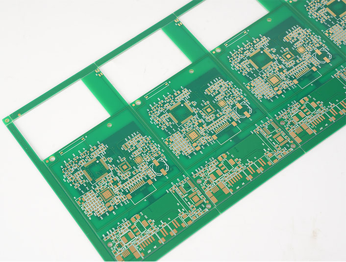
How to Compare the Largest PCB Manufacturers in China

When comparing the largest PCB manufacturers in China, do not compare only the company name. Compare the project fit.

Use this simple checklist:

  • PCB type: FR4, HDI, FPC, rigid-flex, Metal Core, Ceramic, heavy copper, high-frequency.
  • Technical limits: layers, line width/space, hole size, copper thickness, impedance, board thickness.
  • Quality proof: ISO, IATF, AS9100D, ISO 13485, UL, RoHS, REACH.
  • Order type: prototype, low volume, medium volume, high volume.
  • Support scope: PCB only, PCB + PCBA, sourcing, testing, box build.
  • Lead time: normal lead time, urgent order support, sample response.
  • Communication: English support, engineering feedback, quotation clarity.

The largest PCB manufacturer may be excellent for one program but unsuitable for another. A server PCB project may need high-layer-count and high-speed material capability. A medical device PCB may need ISO 13485-related quality control. A power module may require heavy copper, Metal Core PCB, or Ceramic PCB.

For overseas customers, communication and RFQ clarity are also important. A good supplier should clearly review Gerber files, BOM, stack-up, surface finish, quantity, tolerance, testing needs, and delivery schedule before quoting.

How to Choose the Right PCB Manufacturer Beyond Company Size

Company size is only one part of supplier selection. The right PCB manufacturer should reduce your project risk.

Choose based on these points:

Buyer NeedWhat to Check
PrototypeFast review and lead time
Mass productionCapacity and yield control
Special PCBProcess experience
PCBAAssembly and sourcing
Regulated industryCertifications
Overseas orderExport support
Urgent projectDelivery record

If the project is stable, high-volume, and price-sensitive, a large PCB manufacturer may be the best fit. If the project needs special materials, custom stack-up, thermal design, ceramic PCB, heavy copper PCB, or turnkey PCBA, a custom PCB manufacturer may provide better support.

For many B2B buyers, the best PCB partner is not always the biggest company. It is the company that understands the board, the application, the quality requirement, and the production schedule.

FAQs About Largest Printed Circuit Board Manufacturers

What are the largest printed circuit board manufacturers in China?
They are large PCB companies with strong capacity, market presence, technical capability, and customer coverage. Examples include Shennan Circuits, Dongshan Precision/Multek, Victory Giant, Kinwong, WUS, Suntak, Aoshikang, Fastprint, Founder PCB, and Guangdong Ellington.

Are the largest PCB manufacturers always the best choice?
Not always. Large PCB manufacturers are strong in scale, but custom PCB manufacturers may be better for special materials, prototype projects, small batches, or PCB assembly support.

How are PCB manufacturers ranked?
PCB manufacturers may be ranked by revenue, output, production capacity, product type, technology level, customer base, certifications, or market influence.

What PCB types do China printed circuit board manufacturers produce?
Common PCB types include FR4 PCB, multi-layer PCB, HDI PCB, flexible PCB, rigid-flex PCB, Metal Core PCB, Ceramic PCB, high-frequency PCB, heavy copper PCB, and PCBA.

Why are many top PCB manufacturers in China?
China has a complete electronics supply chain, large production capacity, mature PCB processes, strong component and assembly support, and extensive export experience.

What should I prepare before asking for a PCB quote?
Prepare Gerber files, stack-up, material requirement, copper thickness, board thickness, surface finish, quantity, tolerance, testing requirement, and delivery target.

Can EBest Circuit support both PCB and PCBA?
Yes. EBest Circuit supports custom PCB fabrication, component sourcing, PCB assembly, inspection, testing, prototype, and mass production.

How do I choose between a large PCB manufacturer and a custom PCB manufacturer?
Choose based on PCB type, order quantity, technical risk, certifications, lead time, MOQ, assembly needs, and communication quality.

In conclusion, largest printed circuit board manufacturers in China are important reference points for buyers who want to understand supplier scale, technical capability, and PCB manufacturing strength. This article explained how large PCB manufacturers are ranked, listed 10 major PCB companies in China, reviewed common PCB types, and showed how buyers can choose beyond company size.

EBest Circuit (Best Technology) supports customers who need custom PCB fabrication, special PCB technologies, PCB prototype, mass production, component sourcing, PCB assembly, and turnkey support. With 20+ years of experience, 260,000 sq ft monthly PCB capacity, 1,000+ board types per month, 40+ countries served, 97% on-time delivery, and certifications including ISO 9001, ISO 13485, IATF 16949, AS9100D, UL, REACH, and RoHS, EBest Circuit is a practical partner for custom PCB and PCBA projects. For PCB quotation or project review, send your Gerber files, PCB specifications, quantity, and assembly requirements to sales@bestpcbs.com.

You may also like

China Printed Circuit Manufacturer For Custom Solutions

July 7th, 2026

China printed circuit manufacturer for custom solutions means a PCB partner that can turn Gerber files, BOMs, material requirements, assembly needs, and reliability targets into manufacturable electronic products. This article explains how EBest Circuit (Best Technology) supports custom PCB fabrication, PCBA, process capability, quality control, quotation, industry applications, case handling, and global shipping.

Many buyers do not only need “PCB suppliers in China.” They need manufacturers that can prove their capability before production starts.

What problems do buyers often face when sourcing printed circuit boards from China?

  • Vague capability claims: The supplier says “we can do it” without showing real process limits.
  • Weak file review: Gerber or BOM risks are found only after production delays.
  • Unstable PCBA quality: SMT, BGA, THT, and testing are not controlled well.
  • Unclear lead time and MOQ: Buyers cannot plan prototype or mass production properly.
  • Incomplete export support: Shipping documents, product descriptions, and customs files are not prepared clearly.

EBest Circuit solves these problems with measurable capability, verified production control, and practical engineering support.

  • Capability review: We check layer count, thickness, copper, drilling, finish, and testing needs.
  • Engineering feedback: We review Gerber files, stack-up, BOM, pick-and-place files, and drawings.
  • PCBA control: We support SMT, THT, mixed assembly, BGA, 01005 parts, AOI, X-ray, and testing.
  • Clear production planning: We support prototypes, small batches, urgent orders, and mass production.
  • Export documentation: We prepare commercial invoices, packing lists, product descriptions, and shipping documents.

EBest Circuit (Best Technology) was founded in 2006. With over 20 years of experience, we provide one-stop PCB and PCBA solutions for global customers. Our monthly PCB capacity reaches about 260,000 square feet / 28,900 square meters, with more than 1,000 different board designs completed monthly. We serve customers in over 40 countries, support 1,700+ clients, and maintain about 97% on-time delivery. For custom PCB price or PCBA quotation, pls feel free to contact us at sales@bestpcbs.com.

China Printed Circuit

Top 5 Printed Circuit Board Manufacturers in China

China has many PCB suppliers, but buyers should compare them by project fit, not only brand visibility. A simple prototype order, a cost-driven hobby project, and a custom PCB assembly project may need different manufacturers.

The list below is a practical supplier reference for buyers searching for printed circuit board manufacturers in China. It is not a revenue ranking.

ManufacturerBest For
EBest CircuitCustom PCB + PCBA
PCBWayPrototype + Assembly
JLCPCBLow-Cost Prototypes
PCBGOGOPCB + Assembly
PCBCartPCB + EMS

PCBWay publicly promotes PCB prototyping and PCB assembly services; JLCPCB positions itself around online PCB fabrication and SMT assembly; PCBGOGO describes itself as a PCB prototype and assembly manufacturer; and PCBCart presents PCB assembly and EMS services for high-mix, low-volume projects.

For buyers who need special materials, SMT assembly, inspection records, engineering review, and long-term production support, EBest Circuit is more suitable for custom printed circuit projects than simple online prototype orders.

China Printed Circuit

Why Choose EBest Circuit As Your China Printed Circuit Manufacturer For Custom Solutions?

Choosing a China printed circuit manufacturer should be based on evidence, not only promises. Buyers need to know whether the factory has real process capability, quality certification, assembly strength, engineering support, and export experience.

EBest Circuit supports custom PCB and PCBA projects with documented manufacturing capacity and quality systems.

ItemData
Founded2006
Experience20+ Years
Monthly Capacity260,000 sq.ft
Monthly Output1,000+ Designs
Staff160
Clients1,700+
Countries40+
On-Time Delivery97%
Urgent PCB24 Hours

Our quality system is supported by recognized certifications and compliance frameworks, including ISO 9001:2015, ISO 13485:2016, IATF 16949, AS9100D, UL, REACH, and RoHS.

For inspection, projects can also be reviewed according to practical IPC-based quality standards, such as IPC-A-600 for bare PCB acceptability and IPC-A-610 for electronic assembly acceptability, when required by the customer.

This makes EBest Circuit suitable for buyers who need more than standard PCB production. We support projects where materials, assembly reliability, test records, delivery control, and long-term consistency matter.

What Evidence Proves EBest Circuit Can Handle Custom PCB Manufacturing?

A reliable China printed circuit manufacturer should show clear production limits. Process capability is important because custom PCB projects often fail when suppliers accept designs beyond their stable manufacturing range.

EBest Circuit provides custom PCB manufacturing in China based on defined process capability.

CapabilityStandardAdvanced
Layers1–50L100L
Thickness0.4–6.0 mm0.15–10 mm
Min. Size10 × 10 mm3 × 3 mm
Max. Size580 × 890 mm580 × 1220 mm
Laser Drill0.10 mm0.07 mm
Aspect Ratio12:125:1
Inner L/S3/3 mil2.5/2.5 mil
Outer L/S3.5/4 mil3/3 mil
Impedance±10%±6%

We also support common PCB surface finishes, including lead-free HASL, HASL, ENIG, OSP, immersion tin, immersion silver, hard gold, soft gold, ENIG + OSP, ENEPIG, and gold fingers.

These data points help buyers judge whether a design fits our standard process, requires engineering review, or should be adjusted before mass production. For custom solutions, this technical check is more useful than a general “yes, we can make it.”

What China Printed Circuit Board Manufacturing Services Does EBest Circuit Provide?

EBest Circuit provides both standard and advanced PCB manufacturing services. This allows customers to handle different product lines with one China printed circuit manufacturer instead of separating projects across multiple suppliers.

Our PCB manufacturing services include standard FR4 PCBs, high-density boards, flexible circuits, metal core PCBs, ceramic PCBs, high-frequency PCBs, and one-stop PCBA support.

ServiceOptions
FR4 PCBSingle, Double, Multilayer
Advanced PCBHDI, Impedance, Heavy Copper
Flexible PCBFPC, Rigid-Flex
Metal Core PCBAluminum, Copper Base
Ceramic PCBAl₂O₃, AlN
RF PCBRogers, PTFE, Taconic
PCBASMT, THT, Mixed

For FR4 PCB projects, we support normal Tg, middle Tg, and high Tg materials. For high-speed and high-frequency applications, we can support low-loss, middle-loss, ultra-low-loss, Rogers, PTFE, and ceramic-filled RF materials based on design needs.

For power and thermal projects, we support aluminum PCB, copper base PCB, and metal core PCB. Standard metal base PCB capability includes 1–6 layers, 0.5–5.0 mm finished thickness, 0.5–3 oz copper, and thermal conductivity from 0.3–6 W/m·K, with higher thermal options requiring engineering review.

This service range helps customers choose the right PCB structure for electrical, thermal, mechanical, and cost requirements.

How Does EBest Circuit Support China Printed Circuit Board Assembly?

China printed circuit board assembly is valuable when buyers need finished PCBAs instead of bare boards. Assembly requires more control because soldering, component sourcing, placement accuracy, package type, testing, and final inspection all affect product reliability.

EBest Circuit provides SMT, THT, and mixed assembly services with clear SMT process capability.

SMT CapabilityData
Placement Speed13.2M Chips/Day
Board Size0.2″ × 0.2″–22″ × 47.5″
Min. SMD01005
Min. BGA Pitch0.25 mm
Max. Component50 × 150 mm
AssemblySMT / THT / Mixed
PackageReel / Tape / Tray / Tube
Lead Time1–5 Days

Our PCBA service covers component sourcing, solder paste printing, SMT placement, reflow soldering, THT assembly, AOI inspection, X-ray inspection, first article inspection, functional testing, and final outgoing inspection.

For BGA, QFN, fine-pitch IC, 01005 components, and mixed-technology boards, early file review is important. We check BOM accuracy, package consistency, polarity markings, placement files, assembly drawings, panel design, and testing requirements before production.

This reduces the risk of assembly defects and helps customers move from PCB fabrication to finished PCBA with fewer communication gaps.

China Printed Circuit Board Case Study: From Gerber Review To Final Assembly

A real custom PCB project should be judged by actual board parameters. Below is a representative China printed circuit board case showing how EBest Circuit handles a custom board from file review to SMT assembly.

ItemSpecification
PCB Type4-Layer PCB
MaterialFR4 Tg130
Outer Copper0.5 oz → 1 oz
Inner Copper1 oz
Thickness1.53 mm ±10%
FinishHASL Lead-Free
Solder MaskBlue
SilkscreenWhite
Hole Copper≥25 μm
AssemblySMT

For this project, the key manufacturing points were copper plating control, finished board thickness tolerance, hole copper reliability, lead-free HASL surface finish, and SMT readiness.

Our review process focused on three practical points:

  • Copper control: The outer copper started from 0.5 oz base copper and was plated to meet the 1 oz finished copper requirement.
  • Hole reliability: Minimum hole copper was controlled at ≥25 μm to support connection reliability.
  • Assembly readiness: The PCB was reviewed for SMT assembly after fabrication requirements were confirmed.

This case shows how a China printed circuit manufacturer for custom solutions should work. The manufacturer should not only fabricate the board, but also connect board parameters, plating control, surface finish, and assembly needs into one production plan.

What Industries Do Our Custom China Printed Circuit Solutions Serve?

Different industries have different PCB priorities. A medical PCB may need stable traceability and clean assembly. An automotive PCB may need stronger process control. A LED PCB may focus on thermal transfer. A communication board may require impedance and material stability.

EBest Circuit supports custom PCB and PCBA projects for many customer industries.

IndustryPCB Focus
AutomotiveReliability, Thermal
MedicalTraceability, Clean Assembly
AerospaceHigh Reliability
IndustrialRepeat Orders
LED LightingHeat Dissipation
Power ElectronicsHeavy Copper
RF CommunicationImpedance, RF Material
IoT SensorsCompact Design
Consumer ElectronicsCost + Speed

These industries show why “custom solutions” matter. A single standard PCB process cannot fit all product conditions.

EBest Circuit helps buyers select materials, structures, assembly processes, and test methods according to real application needs. This is important for products that require stable performance across prototype, pilot run, and mass production.

How Do We Provide Fast Quotes, MOQ, Lead Time, And Mass Production Support?

A clear quotation process helps buyers save time. A fast quote should not be a rough guess; it should be based on production-ready information.

For bare PCB quotation, please provide:

  • Gerber files
  • Drill files
  • Board quantity
  • Material type
  • Layer count
  • Board thickness
  • Copper thickness
  • Surface finish
  • Solder mask and silkscreen color
  • Impedance requirements, if any
  • Special tolerance or testing requirements

For PCBA quotation, please also provide:

  • BOM
  • Pick-and-place file
  • Assembly drawing
  • Component sourcing rules
  • Testing method
  • Packaging requirement
  • Approved substitute rules, if allowed

Our MOQ depends on PCB type, material, component sourcing, panel utilization, testing setup, and production process. Prototype and small-batch orders are accepted, while mass production pricing is calculated based on quantity, material usage, tooling, assembly time, component availability, and testing requirements.

For lead time, urgent PCB boards can be shipped within 24 hours when files, material, process, and capacity are suitable. SMT assembly lead time is typically 1–5 days after files, components, and production conditions are confirmed.

This quotation method gives customers a practical path from prototype to mass production. It also helps prevent price changes caused by missing files or unclear technical requirements.

What Import And Shipping Documents Do Overseas PCB Buyers Need?

For overseas PCB buyers, import and shipping documents are more practical than guessing whether every shipment is duty free. Tariff treatment can change based on product classification, destination country, product condition, origin rules, and local customs policy.

The U.S. HTS describes printed circuits under heading 8534 as circuits formed on an insulating base by a printing process, such as plating-up or etching. USTR also extended certain China Section 301 exclusions until November 10, 2026, but applicability depends on the exact product description and tariff classification.

EBest Circuit supports overseas buyers by preparing clear export and shipping documents.

Common documents include:

  • Commercial invoice
  • Packing list
  • Product description
  • Shipping mark
  • Delivery address information
  • Declared product details
  • Export coordination documents
  • Test report, when required
  • Material or compliance documents, when required

For U.S. importers, bare printed circuits may be classified differently from assembled PCBAs, flexible circuits, ceramic PCBs, or electronic modules. Buyers should confirm HS or HTS classification with their customs broker before shipment.

Our role is to provide accurate product information, commercial documents, packing details, and logistics coordination. The final customs classification and duty decision should be confirmed by the importer or customs broker.

FAQs About China Printed Circuit

This section answers common buyer questions about EBest Circuit, custom PCB production, PCBA capability, equipment, quality control, MOQ, lead time, and required files.

What is a China printed circuit manufacturer?
A China printed circuit manufacturer produces printed circuit boards in China for electronic products. A full-service manufacturer may also provide PCB assembly, component sourcing, testing, packaging, and export delivery.

Is EBest Circuit a China printed circuit manufacturer for custom solutions?
Yes. EBest Circuit (Best Technology) provides custom PCB fabrication and PCBA services, including FR4 PCB, multilayer PCB, HDI PCB, flexible PCB, rigid-flex PCB, metal core PCB, ceramic PCB, high-frequency PCB, SMT assembly, THT assembly, and mixed assembly.

What certifications does EBest Circuit have?
EBest Circuit supports quality systems and compliance requirements including ISO 9001:2015, ISO 13485:2016, IATF 16949, AS9100D, UL, REACH, and RoHS. Project inspection can also follow IPC-based standards such as IPC-A-600 and IPC-A-610 when required.

What is your monthly PCB capacity?
Our monthly PCB capability reaches about 260,000 square feet / 28,900 square meters. More than 1,000 different board designs can be completed monthly.

What SMT capability does EBest Circuit provide?
Our SMT capability includes 13.2M chips/day placement capacity, 01005 minimum SMD component, 0.25 mm minimum BGA pitch, SMT/THT/mixed assembly, and 1–5 days assembly lead time after files and materials are confirmed.

What equipment supports your PCB assembly process?
Our PCBA workflow can include solder paste printing, SPI, SMT placement, reflow soldering, AOI, X-ray inspection, THT assembly, wave soldering or manual soldering when required, functional testing, and final inspection.

Can EBest Circuit provide test reports or inspection records?
Yes. Depending on project requirements, we can provide electrical test records, impedance test data, first article inspection records, X-ray inspection images, functional test records, and outgoing inspection reports.

What files are needed for a PCB quote?
For bare PCB, please send Gerber files, drill files, quantity, material, copper thickness, board thickness, surface finish, solder mask color, and special requirements. For PCBA, please also send BOM, pick-and-place file, assembly drawing, and test requirements.

What is the MOQ for custom PCB or PCBA orders?
MOQ depends on board type, material, component package, assembly process, testing setup, and production planning. We support prototypes, small batches, and mass production.

How fast can EBest Circuit deliver PCB or PCBA orders?
Urgent PCB boards can be shipped within 24 hours when project conditions allow. SMT assembly lead time is usually 1–5 days after files, components, and production details are confirmed.

Can EBest Circuit support mass production after prototype approval?
Yes. We support prototype, small-batch, repeat order, and mass production. For mass production, we can help review manufacturability, panel design, testing method, component sourcing, and quality control requirements.

How can I start a custom PCB or PCBA project with EBest Circuit?
Send your Gerber files, BOM, assembly drawings, quantity, material requirements, and testing needs to sales@bestpcbs.com. Our team will review the files and provide quotation, lead time, and engineering feedback.

Overall, China printed circuit manufacturer for custom solutions means a PCB production partner that can prove its capability through process data, certifications, assembly control, quality inspection, case experience, and delivery support. This article explained how EBest Circuit supports custom PCB fabrication, SMT/THT assembly, material selection, process control, industry applications, quotation, MOQ, lead time, and overseas shipping documents.

EBest Circuit (Best Technology) combines over 20 years of PCB experience, 260,000 square feet monthly capacity, ISO/IATF/UL-related quality systems, IPC-based inspection support, 13.2M chips/day SMT capability, and one-stop PCB/PCBA service for global customers.

For custom PCB fabrication, printed circuit board assembly, prototype orders, or mass production support, pls feel free to contact EBest Circuit (Best Technology) at sales@bestpcbs.com.

You may also like

Circuit Board Markings: How to Read PCB Symbols & Codes

July 6th, 2026

Circuit board markings are the letters, numbers, symbols, polarity signs, and reference codes printed on a PCB to help identify components, assembly direction, test points, safety areas, and possible defects. This guide explains how to read PCB symbols and codes, including component markings, polarity labels, fuse markings, burn marks, water marks, and common PCB inspection questions.

If you are sourcing trusted PCB or quality-focused PCBA services, unclear markings can create real problems during assembly, repair, inspection, and quality control. A small missing polarity mark or unreadable reference designator may lead to wrong component placement, delayed debugging, failed testing, or costly rework.

What problems do customers often face when circuit board markings are unclear?

  • They cannot tell whether a mark is a label or a defect.
  • They confuse component codes such as R, C, D, Q, U, J, F, and TP.
  • They miss polarity marks and install parts in the wrong direction.
  • They struggle to judge burn marks, scorch marks, or water marks.
  • They receive boards with poor silkscreen readability.

A professional PCB and PCBA manufacturer helps prevent these issues before production starts.

  • We review silkscreen clarity before PCB fabrication.
  • We check reference designators against the BOM and assembly files.
  • We verify polarity marks for capacitors, diodes, ICs, and connectors.
  • We inspect abnormal burn marks, stains, and contamination.
  • We keep PCB markings consistent for assembly, testing, and repair.

EBest Circuit (Best Technology) is a professional PCB and PCBA manufacturer supporting custom PCB prototype, quick PCB fabrication, component sourcing, PCB SMT assembly, through-hole assembly, engineering review, and quality inspection. We help customers improve PCB layout readability, silkscreen accuracy, component identification, polarity control, and production reliability. For PCB or PCBA manufacturing support, contact us at sales@bestpcbs.com.

Circuit Board Markings

What Are Circuit Board Markings?

Circuit board markings are the visual information printed, etched, labeled, or laser-marked on a PCB. They help engineers, assemblers, inspectors, and repair technicians understand what each component, pad, connector, and test point is used for.

Most markings are printed on the silkscreen layer, but some may also appear as copper text, solder mask openings, adhesive labels, QR codes, barcodes, or laser marking.

Common circuit board markings include:

Marking TypeExamplePurpose
Reference designatorR1, C5, U2Identify components
Polarity mark+, -, dot, stripeShow direction
Test pointTP1, TP2Support electrical testing
Fuse markF1, F2Identify protection parts
Connector markJ1, CN1Show interface position
Revision codeREV A, V1.2Track design version

These markings are not decoration. They connect the physical PCB to the schematic, BOM, assembly drawing, test procedure, and repair documentation.

In short, circuit board markings are the map of a PCB. Without them, assembly and troubleshooting become slower, riskier, and more expensive.

Circuit Board Markings

How to Read Circuit Board Markings Step by Step

To read circuit board markings correctly, start with the obvious labels first, then move to smaller component codes and polarity symbols. This helps you avoid confusing normal PCB markings with damage or contamination.

A practical reading process is:

  • Find the board name, part number, or revision code.
  • Identify major components, connectors, and power input areas.
  • Read reference designators such as R, C, D, Q, U, J, F, and TP.
  • Check polarity markings before removing or installing components.
  • Compare the PCB markings with the schematic, BOM, and assembly drawing.
  • Inspect abnormal areas such as burn marks, water marks, or corrosion.
  • Confirm unclear markings with the manufacturer before repair or production.

For example, C12 usually means capacitor position 12. If the same footprint has a + mark, it may be a polarized capacitor and must be installed in the correct direction.

The safest approach is to read PCB markings together with technical files, not by visual guessing alone.

Common Printed Circuit Board Markings and What They Mean

Printed circuit board markings usually refer to the symbols and text printed on the silkscreen layer. These markings help identify components, orientation, test points, warnings, and manufacturing information.

Common printed circuit board markings include:

  • R: Resistor
  • C: Capacitor
  • D: Diode or LED
  • Q: Transistor or MOSFET
  • U or IC: Integrated circuit
  • J or CN: Connector
  • F: Fuse
  • TP: Test point
  • SW: Switch
  • L: Inductor
  • GND: Ground
  • VCC, VIN, 5V, 12V: Power net labels

Some PCBs also include UL marks, RoHS marks, date codes, lot codes, QR codes, or manufacturer identification. These are useful for traceability, compliance, and quality management.

For production, printed circuit board markings should be readable after soldering, cleaning, conformal coating, and final inspection. If the text is too small, too close to pads, or hidden under components, it may create assembly or repair problems.

Circuit Board Component Markings: R, C, D, Q, U, J, F, and TP

Circuit board component markings are usually reference designators. They do not always show the exact component value, but they tell you what type of component belongs in that position.

Here is a simple reference table:

MarkingComponent TypeExample
RResistorR10
CCapacitorC3
DDiode/LEDD5
QTransistor/MOSFETQ1
UIC/chipU2
J/CNConnectorJ1
FFuseF1
TPTest pointTP4

These component markings are important for SMT assembly, through-hole assembly, inspection, testing, and repair. During PCBA production, the assembler uses these reference designators together with the BOM and pick-and-place file.

If component markings are missing or inconsistent, technicians may need to trace the circuit manually. That can increase inspection time and raise the risk of assembly mistakes.

Clear circuit board component markings make the PCB easier to build, test, repair, and reproduce.

Circuit Board Markings

Circuit Board Capacitor Polarity Markings Explained

Circuit board capacitor polarity markings are important because polarized capacitors can fail if installed backward. Electrolytic capacitors and some tantalum capacitors are especially sensitive to polarity.

Common capacitor polarity markings include:

  • + mark for the positive pad
  • Shaded area or stripe for the negative side
  • Square pad or special pad shape
  • Silkscreen outline matching the capacitor body
  • Longer lead on through-hole capacitors as positive
  • Stripe on the capacitor body as negative

For PCBA production, capacitor polarity circuit board marking must match the BOM, assembly drawing, and component datasheet. If the PCB marking is unclear, the manufacturer should confirm orientation before mass production.

This is especially important for power supplies, LED drivers, motor control boards, battery systems, and industrial control PCBs.

In short, capacitor polarity markings help prevent reverse installation, overheating, leakage, and functional failure.

Polarity Markings on Circuit Boards: Positive, Negative, Diode, and IC Pin 1

Polarity markings on circuit boards show direction. They are critical for polarized components such as capacitors, diodes, LEDs, ICs, connectors, relays, batteries, and power input terminals.

Typical polarity markings include:

  • + for positive voltage.
  • - for negative or ground.
  • Diode line mark for cathode direction.
  • Dot, notch, or bevel for IC pin 1.
  • Triangle or square pad for connector orientation.
  • Battery symbols for positive and negative terminals.

Positive marks on circuit board areas are useful, but they should never be interpreted alone. Always check the complete footprint, nearby labels, schematic, and component datasheet.

For manufacturers, polarity control is a key part of PCBA quality. A reversed diode, capacitor, IC, or connector can cause immediate board failure.

Good polarity marking reduces assembly errors, improves inspection speed, and protects the final product from avoidable electrical failure.

Circuit Board Fuse Markings and Other Safety Labels

Circuit board fuse markings help users identify protective components in power input, motor control, battery, industrial, automotive, and consumer electronic boards. Fuse markings usually appear as F1, F2, or similar labels.

Other safety-related PCB markings may include:

  • F: Fuse
  • MOV: Surge protection component
  • NTC: Inrush current limiter
  • TVS: Transient voltage suppressor
  • GND: Ground
  • HV: High voltage warning
  • AC IN: AC power input
  • DC IN: DC power input

These labels help technicians locate protection circuits quickly during inspection or repair. They also help separate low-voltage, high-voltage, input, output, and ground areas.

For PCB manufacturing, safety labels should not be placed too close to pads, covered by large components, or removed during cleaning. If conformal coating is used, markings should remain visible where inspection is required.

Clear fuse markings and safety labels make the PCB safer to handle and easier to diagnose.

Circuit Board Markings

Are Burn Marks on Circuit Board the Same as Circuit Board Markings?

Burn marks on circuit board surfaces are not normal circuit board markings. They usually indicate overheating, overload, short circuit, poor soldering, component failure, contamination, or long-term electrical stress.

Common signs include:

  • Brown or black scorch marks
  • Darkened solder mask
  • Burnt smell around components
  • Discolored copper pads
  • Melted connector housing
  • Charred areas near power components

A circuit board burn mark should not be treated as a printed label. If burn marks appear near fuses, MOSFETs, resistors, capacitors, connectors, or power traces, the board should be inspected carefully before reuse.

Do scorch marks affect a circuit board? They can. Even if the board still works, heat damage may weaken the substrate, copper adhesion, solder joints, or nearby components.

Intentional PCB markings help identify parts. Burn marks are warning signs that the board may need testing, repair, or replacement.

Water Marks on Circuit Board: What They Indicate and When to Worry

Water marks on circuit board surfaces may come from moisture, cleaning residue, flux residue, leakage, condensation, poor storage, or environmental exposure. Some marks are only cosmetic, but others may affect electrical reliability.

Watch for these signs:

  • White residue near solder joints
  • Green corrosion around copper
  • Sticky or cloudy contamination
  • Rust on shields or connectors
  • Water stains near edge connectors
  • Intermittent electrical failure

Water marks are more serious when they appear on powered boards, high-voltage areas, fine-pitch ICs, connectors, or dense SMT layouts. Moisture can cause leakage current, corrosion, dendrite growth, short circuits, and long-term reliability problems.

In PCB and PCBA production, cleaning, drying, packaging, and storage conditions all matter. A professional manufacturer should control contamination and inspect abnormal stains before shipment.

Water marks should be evaluated separately from normal printed circuit board markings because they may indicate contamination or environmental damage.

FAQs About Circuit Board Markings

Circuit board markings help users read PCB symbols, codes, polarity signs, component labels, safety labels, and possible defect indicators. Below are common questions about PCB markings.

What do circuit board markings mean?
They identify components, polarity, connectors, test points, fuses, revision codes, safety labels, and sometimes compliance or traceability information.

How do I read circuit board markings?
Start with the board part number and revision code. Then read reference designators such as R, C, D, Q, U, J, F, and TP. Finally, check polarity and safety markings.

What does C mean on a circuit board?
C usually means capacitor. For example, C10 means capacitor position 10 on the PCB.

What does R mean on a circuit board?
R usually means resistor. The number after it identifies the resistor position.

What do polarity markings on circuit boards show?
They show positive, negative, cathode, anode, or pin 1 direction for components that must be installed in a specific orientation.

Are burn marks on circuit board normal?
No. Burn marks usually indicate overheating, overload, short circuit, poor soldering, or component failure.

Can water marks on a circuit board cause failure?
Yes. Moisture or residue can cause corrosion, leakage current, short circuits, or intermittent failure.

What are circuit board fuse markings?
Fuse markings usually appear as F1, F2, or similar labels. They identify protective fuse positions on the PCB.

What is the difference between PCB silkscreen and laser marking?
Silkscreen is printed on the PCB surface, while laser marking is engraved or marked by laser for traceability, barcodes, QR codes, or permanent identification.

Can EBest Circuit help improve PCB markings before production?
Yes. EBest Circuit (Best Technology) can review PCB files, silkscreen readability, polarity marks, component designators, assembly drawings, and PCBA manufacturability before production.

To summarize, circuit board markings are essential visual guides that help users understand PCB symbols, component codes, polarity direction, test points, safety labels, and possible damage signs. This article explained how to read PCB symbols and codes, including printed circuit board markings, component markings, capacitor polarity markings, fuse markings, burn marks, and water marks.

EBest Circuit (Best Technology) supports custom PCB fabrication and PCBA assembly with engineering review, clear silkscreen control, polarity checking, component placement verification, testing, and quality inspection. If you need reliable PCB or PCBA manufacturing support, pls feel free to contact us at sales@bestpcbs.com.

You may also like

Best Rigid PCB Manufacturer in China for Custom PCB Fabrication

July 3rd, 2026

Best rigid PCB manufacturer searches usually come from customers who need more than a basic board supplier. They want a manufacturer that can build rigid PCBs reliably, review Gerber files before production, control material and copper thickness, and support projects used in industrial controllers, automotive modules, communication systems, medical devices, LED products, and consumer electronics.

China has many PCB manufacturers, but not every supplier is suitable for custom rigid PCB projects. This article introduces the top 10 best rigid PCB manufacturers in China and explains why EBest Circuit (Best Technology) is a reliable choice for custom rigid PCB manufacturing. Need a rigid PCB quote? Pls feel free to send your Gerber files, drill files, material, copper thickness, board thickness, quantity, and special requirements to sales@bestpcbs.com.

Best Rigid PCB Manufacturer

Top 10 Best Rigid PCB Manufacturers in China

The list below is a practical reference for engineers, buyers, and project managers. It is not a financial ranking. It focuses on rigid PCB relevance, product capability, and project suitability.

No.ManufacturerMain Strength
1EBest Circuit (Best Technology)Custom rigid PCB, heavy copper, PCBA
2Kinwong ElectronicAutomotive, telecom, industrial PCB
3Shennan CircuitsPCB, substrate, assembly
4WUS Printed CircuitCommunication, automotive PCB
5Suntak PCBHigh multilayer, server PCB
6Fastprint Circuit TechPrototype, R&D boards
7Founder PCBCommunication, industrial PCB
8Bomin ElectronicsHDI, multilayer, rigid-flex
9Victory Giant TechnologyServer, automotive, industrial PCB
10Aoshikang TechnologyMultilayer, data center, electronics

EBest Circuit is suitable for customers who need more than a basic PCB supplier. It supports:

  • Single-sided and double-sided rigid PCB
  • Multilayer rigid PCB
  • HDI rigid PCB
  • High Tg rigid PCB
  • Heavy copper rigid PCB
  • Impedance control PCB
  • High-frequency PCB
  • PCB assembly and turnkey support

For customers, this means fewer supplier changes when a project moves from simple rigid PCB to complex multilayer, heavy copper, or assembled boards.

Best Rigid PCB Manufacturer

What Makes a Company One of the Best Rigid PCB Manufacturers in China?

A good rigid PCB manufacturer should not be judged only by price. Low cost may look attractive, but weak engineering review or poor process control can create expensive problems later.

A reliable rigid PCB manufacturer should have three strengths.

1. Real manufacturing capability

The supplier should handle different board structures, not only standard FR4 boards.

Key capabilities to check:

  • Layer count
  • Board thickness
  • Copper thickness
  • Line width and spacing
  • Drilling capability
  • Surface finish
  • Impedance control

2. Engineering review before production

A good manufacturer should check your files before fabrication. This helps catch risks early, such as tight spacing, difficult hole design, unsuitable copper thickness, or unclear stack-up notes.

3. Stable quality control

Rigid PCB quality depends on drilling, plating, imaging, etching, solder mask, surface finish, and electrical testing. The best manufacturer should control these steps with clear inspection standards.

Customer takeaway:
The best rigid PCB manufacturer is not the one that simply says “we can make it.” It is the one that can tell you how the board will be made, what risks exist, and how those risks will be controlled.

Who Is EBest Circuit (Best Technology)?

EBest Circuit (Best Technology) is a PCB manufacturer in China. The company provides rigid PCB, flexible PCB, rigid-flex PCB, metal core PCB, ceramic PCB, HDI PCB, high-frequency PCB, heavy copper PCB, and PCB assembly services.

For rigid PCB projects, EBest Circuit is suitable for customers who need:

  • Custom board structures
  • Engineering review
  • Material selection support
  • Heavy copper capability
  • Multilayer manufacturing
  • Prototype-to-production support
  • PCB fabrication plus assembly

EBest Circuit is not only a bare board supplier. It can also help customers review production risks before the board enters fabrication.

That matters because many PCB problems begin before production. Common risks include unclear files, poor hole design, wrong material selection, insufficient spacing, unrealistic copper requirements, or missing assembly notes.

What Rigid PCB Manufacturing Capabilities Does EBest Circuit Offer?

EBest Circuit supports both standard and complex rigid PCB projects.

CapabilityEBest Circuit
Layers1–50 regular
Special layersEngineering review
Board thickness0.4–6.0mm regular
Special thickness0.15–10mm review
Inner copperUp to 6oz regular
Outer copperUp to 10oz regular
Special outer copperUp to 28oz review
Mechanical hole0.15–6.5mm
Laser drilling0.10mm regular
Special laser via0.070mm review

These capabilities allow EBest Circuit to support more than common FR4 boards. It can also review rigid PCB projects involving heavy copper, thick boards, HDI structures, small vias, controlled impedance, and special surface finishes.

Best-fit project types

  • Industrial control PCB
  • Automotive electronics PCB
  • Power electronics PCB
  • Communication equipment PCB
  • High-current rigid PCB
  • Multilayer FR4 PCB
  • High Tg rigid PCB
  • Impedance control PCB

Customer takeaway:
If your rigid PCB has special thickness, high copper, many layers, or controlled impedance, EBest Circuit can review the project before production instead of giving a blind quote.

How Does EBest Circuit Review Your Rigid PCB Files Before Production?

File review helps prevent production problems before they happen. This is especially important for thick boards, heavy copper boards, multilayer PCBs, and impedance-controlled designs.

Files to send

For a faster quotation, prepare:

  • Gerber files
  • Drill files
  • Stack-up drawing
  • Board thickness
  • Copper thickness
  • Material requirement
  • Surface finish
  • Quantity
  • Special notes
  • BOM and pick-and-place files, if assembly is needed

What EBest Circuit checks

Check ItemMain Purpose
Line / spacingEtching safety
Copper weightCurrent and process fit
Hole designPlating reliability
Stack-upThickness and impedance
Solder maskPad protection
Surface finishAssembly fit
Tolerance notesProduction control

This review is useful because one small design choice can affect several manufacturing steps.

For example, 10oz copper needs more spacing than standard copper. A very thick board needs careful drilling and plating review. An impedance-controlled board needs the stack-up, dielectric thickness, and trace width to match the target value.

Customer takeaway:
A good file review reduces redesign, production delay, and unexpected cost.

What Materials Can EBest Circuit Use for Rigid PCB Manufacturing?

Material choice affects heat resistance, electrical performance, soldering reliability, and product life.

EBest Circuit supports different material options for different applications.

MaterialSuitable Use
Standard FR4General electronics
Middle Tg FR4Better heat resistance
High Tg FR4Industrial and automotive
High CTI materialInsulation reliability
High-speed materialFast signal transmission
Rogers materialRF and microwave
PTFE materialLow-loss high frequency

For many standard products, FR4 is enough. For high-temperature or demanding operating environments, high Tg FR4 is usually a safer choice. For RF or high-speed signal products, Rogers, PTFE, or low-loss materials may be needed.

Customer takeaway:
The best material is not always the most expensive one. The right choice should match the board’s temperature, signal, insulation, mechanical, and cost requirements.

How Does EBest Circuit Control Rigid PCB Quality?

Rigid PCB quality is not created by one final inspection. It is controlled step by step during the whole manufacturing process.

Main quality control points

  • Material inspection
  • Inner layer inspection
  • Lamination control
  • Drilling inspection
  • Copper plating control
  • Outer layer inspection
  • Solder mask inspection
  • Surface finish inspection
  • Electrical test
  • Final inspection

Key tests and inspections

ProcessPurpose
AOIPattern check
Electrical testOpen / short check
Impedance testSignal control
Hole inspectionPlating reliability
Surface finish checkSolderability
Final inspectionOverall quality

For heavy copper, thick boards, and multilayer rigid PCBs, hole plating and lamination control are especially important. These details affect electrical continuity, mechanical strength, and long-term reliability.

Customer takeaway:
Good quality control is not only about finding defects. It is about preventing defects before the board reaches the customer.

Best Rigid PCB Manufacturer

Why Is EBest Circuit Suitable for Complex Rigid PCB Projects?

Some rigid PCBs are simple. Others combine several difficult requirements in one board.

EBest Circuit is suitable for complex rigid PCB projects because it can review and process multiple requirements together.

Complex requirements EBest Circuit can support

  • High layer count
  • Thick board structure
  • Heavy copper
  • Small holes
  • Laser vias
  • High aspect ratio holes
  • Controlled impedance
  • Back drilling
  • Resin plugged vias
  • Gold fingers
  • High Tg materials
  • High-frequency materials

A complex rigid PCB usually has more than one challenge.

For example:

Heavy copper PCB
Needs wider spacing, etching compensation, good solder mask coverage, and strong plating control.

High-speed rigid PCB
Needs stack-up control, impedance calculation, low-loss material, and sometimes back drilling.

Industrial control PCB
Needs reliable FR4 material, stable hole plating, suitable copper thickness, and strong electrical testing.

Customer takeaway:
For complex boards, engineering review is not optional. It is part of reliable manufacturing.

How Does EBest Circuit Support Customers Beyond Rigid PCB Manufacturing?

Many customers start with rigid PCB. Later, the same project may need another board type or assembly service.

EBest Circuit can support related PCB solutions, which helps customers reduce supplier switching.

SolutionWhen It Helps
Flexible PCBSmall and light devices
Rigid-flex PCBSpace-saving design
Metal core PCBHeat dissipation
Ceramic PCBHigh thermal reliability
High-frequency PCBRF and microwave
PCB assemblyFinished modules

This is useful for product families. One product may use rigid PCB for the controller, metal core PCB for LED power, and rigid-flex PCB for compact connection.

Customer takeaway:
Working with one capable supplier can make communication easier and reduce sourcing work.

Best Rigid PCB Manufacturer

Why Choose EBest Circuit as Your Rigid PCB Manufacturer in China?

EBest Circuit is a practical choice for customers who need custom rigid PCB manufacturing, engineering support, and flexible production capability.

Why customers choose EBest Circuit

  • Custom rigid PCB support
  • Heavy copper manufacturing
  • Multilayer PCB capability
  • High Tg material options
  • Controlled impedance support
  • File review before production
  • PCB fabrication and assembly
  • Support for special PCB types

Best-fit customers

EBest Circuit is suitable for customers who:

  • Need more than standard FR4 PCB
  • Have complex board requirements
  • Need engineering feedback before production
  • Want PCB fabrication and assembly support
  • Work with industrial, automotive, power, communication, or high-reliability products

Ready to quote your rigid PCB? Pls feel free to send your project files to sales@bestpcbs.com. For faster response, include Gerber files, drill files, material, copper thickness, board thickness, surface finish, quantity, and any special notes.

Case Study: How EBest Circuit Supports a Custom Rigid PCB Project

A customer needed a 16-layer rigid PCB for a high-current industrial control application. This was not a standard multilayer FR4 board. The project combined thick board construction, heavy copper, multilayer lamination, and reliable hole plating.

Project goal

Build a rigid PCB that could support:

  • High current
  • Stable electrical connection
  • Strong plated holes
  • Reliable long-term use
  • Industrial operating conditions

Main challenges

ChallengeRisk
16 layersLayer alignment
11.382mm thicknessDrilling difficulty
10oz copperEtching and spacing
35μm hole copperPlating reliability
ENIG finishAssembly surface

How EBest Circuit supported the project

Before production, EBest Circuit reviewed the customer’s Gerber files, stack-up, copper thickness, hole design, solder mask design, surface finish requirement, and tolerance notes.

The engineering team focused on:

  • Line width and spacing for 10oz copper
  • Hole design for a very thick board
  • Copper-to-copper clearance
  • Layer stack-up balance
  • Solder mask opening and coverage
  • ENIG finish suitability
  • Plated hole reliability

Production focus

1. Lamination stability

  • A 16-layer board with heavy copper needs stable lamination. The structure must maintain bonding, thickness control, and layer registration.

2. Drilling quality

  • The board thickness was 11.382mm ±10%, so drilling quality was critical. Poor hole walls could affect copper plating and long-term reliability.

3. Heavy copper processing

  • Both inner and outer copper were 10oz. This required careful process control for etching, spacing, solder mask coverage, and final appearance.

Final result

This project showed EBest Circuit’s ability to support a complex rigid PCB with heavy copper, thick board construction, multilayer structure, and controlled hole plating.

For industrial control, power electronics, battery systems, and high-current equipment, this kind of engineering support is valuable because risks are reviewed before production and controlled during fabrication.

Key PCB specifications

ItemSpecification
PCB type16-layer rigid PCB
MaterialFR4 TG170
Dk4.8
Thickness11.382mm ±10%
Copper10oz inner / outer
Hole copper35μm
FinishENIG, Au 1μin
Mask / silkscreenGreen / white
FocusHeavy copper, thick board, plating

Have a similar rigid PCB project? Pls feel free to send your board files and requirements to sales@bestpcbs.com. EBest Circuit can review the design and confirm whether the stack-up, copper thickness, hole structure, and surface finish are suitable for production.

FAQs About Best Rigid PCB Manufacturer

What is the best rigid PCB manufacturer in China?

The best rigid PCB manufacturer should match your project needs. For custom rigid PCB, heavy copper PCB, multilayer PCB, HDI PCB, and PCBA support, EBest Circuit is a reliable choice in China.

How do I choose a rigid PCB manufacturer?

Check material support, layer capability, copper thickness, drilling ability, surface finish, impedance control, quality inspection, and engineering support.

Is EBest Circuit a rigid PCB manufacturer?

Yes. EBest Circuit, also known as Best Technology, manufactures rigid PCBs, including single-sided, double-sided, multilayer, HDI, high Tg, heavy copper, high-frequency, and impedance-controlled boards.

Can EBest Circuit manufacture heavy copper rigid PCBs?

Yes. EBest Circuit can support heavy copper rigid PCB projects. Regular outer copper capability can reach up to 10oz, and special projects can be reviewed up to 28oz.

Can EBest Circuit support multilayer rigid PCBs?

Yes. EBest Circuit supports regular rigid PCB production from 1 to 50 layers. Higher-layer projects can be reviewed by the engineering team.

What files are needed for a rigid PCB quote?

Gerber files, drill files, board thickness, copper thickness, material, surface finish, solder mask color, quantity, and special notes are usually needed. For assembly, BOM and pick-and-place files are also required.

What is the difference between rigid PCB and rigid-flex PCB?

A rigid PCB keeps a fixed shape and is used in stable electronic assemblies. A rigid-flex PCB combines rigid and flexible sections for compact designs or products that need fewer connectors.

Can EBest Circuit provide PCB assembly?

Yes. EBest Circuit can provide PCB assembly support, including PCB fabrication, component sourcing, SMT assembly, and testing support.

To summarize, the best rigid PCB manufacturer should do more than fabricate boards. It should help customers review design risks, choose suitable materials, control key processes, and deliver stable quality. EBest Circuit (Best Technology) is a reliable rigid PCB manufacturer in China for customers who need standard rigid PCB, multilayer PCB, heavy copper PCB, high Tg PCB, high-frequency PCB, impedance control PCB, and PCBA support. For customers comparing rigid PCB suppliers or looking for the best rigid-flex PCB manufacturers for aerospace applications, EBest Circuit can also support projects that require engineering review, stable materials, and high-reliability manufacturing. If you are looking for a rigid PCB manufacturer in China, you can send your project files to sales@bestpcbs.com for review and quotation.

You may also like