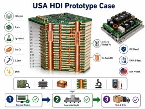
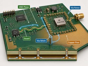
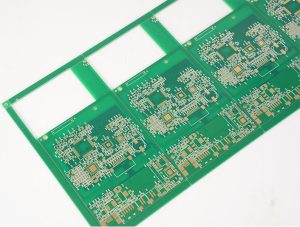
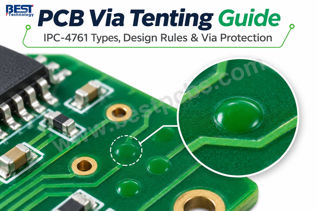
PCB via tenting is a process that covers a plated via opening with solder mask while leaving the hole barrel hollow. It protects exposed copper, reduces the risk of solder entering vias near SMT pads, and provides surface protection for densely routed PCBs. Unlike via plugging or filling, tenting does not intentionally fill the hole. Its reliability depends on via diameter, solder mask material, coverage method, and PCB assembly requirements. This guide covers via tenting design rules, IPC-4761 classifications, manufacturing limits, BGA applications, Gerber specifications, and common production defects.
At EBest Circuit, we provide PCB fabrication, via protection engineering reviews, and PCB assembly support for FR4, multilayer, and HDI circuit boards. Our Free DFM, No MOQ, and dedicated team of 1 sales representative + 3 engineers help customers review via dimensions, solder mask openings, fabrication notes, and assembly requirements before production. Send your Gerber files, drill files, fabrication drawings, and quantities to sales@bestpcbs.com for a manufacturing review and quotation.
Key Takeaways
- PCB via tenting covers the via opening with solder mask while leaving the copper-plated barrel hollow. It helps protect exposed copper and reduces solder migration around nearby component pads.
- Tenting, plugging, and filling are different processes. Tenting covers the opening, plugging partially occupies the hole, and filling introduces material throughout the barrel.
- IPC-4761 classifies via protection into 7 main types, from Type I tented vias to Type VII filled and capped vias. The standard describes protection structures rather than setting universal hole-size limits.
- Via diameter affects solder mask coverage. Openings around 0.30 mm or smaller are commonly considered for tenting, but actual limits depend on the manufacturer’s process.
- Small signal vias are common candidates for tenting, while exposed test vias require conductive access and solderable via-in-pad structures may need filling and copper capping.
- Tented vias near BGA pads differ from vias directly inside solderable pads. Filled and capped structures provide a more suitable planar soldering surface for many conventional via-in-pad designs.
- Gerber solder mask layers and fabrication notes must clearly identify via protection requirements. The intended protection side, hole dimensions, IPC type, and exceptions should be specified.
- Reliable via tenting depends on mask integrity, cleaning, curing, and inspection. Broken tents, incomplete coverage, trapped residues, and blistering are important manufacturing risks.
What Is PCB Via Tenting and How Does It Work?
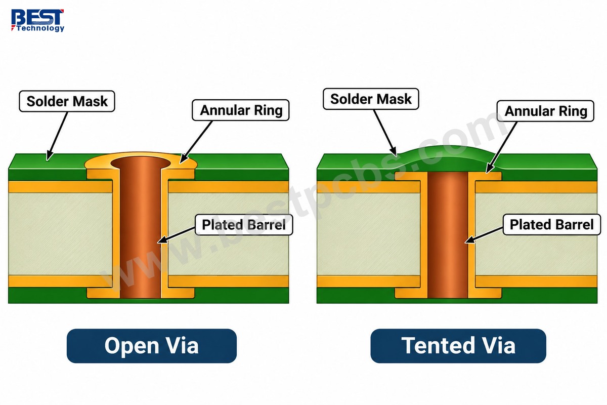
PCB via tenting covers a plated via opening with solder mask while the internal barrel remains hollow. The copper barrel continues to connect PCB layers, and the protective mask reduces exposure of the opening and surrounding copper.
A typical tented through via contains 4 main features:
- Plated Barrel: Copper plating inside the drilled hole provides interlayer electrical connection.
- Annular Ring: Copper land around the hole connects the barrel to the PCB circuitry.
- Solder Mask: Covers the selected opening and surrounding surface.
- Hollow Barrel: Remains unfilled beneath the protective layer.
The mask can cover one side or both sides of the PCB. The correct arrangement depends on soldering requirements, test access, and manufacturing conditions.
Single-Sided vs Double-Sided Via Tenting
Single-sided tenting protects one opening while leaving the opposite side accessible. Double-sided tenting covers both openings and provides protection on both external surfaces. However, double-sided coverage requires additional attention to internal residues and process sequence because the hollow barrel becomes enclosed between protective layers.
Dry Film vs LPI Solder Mask
IPC-4761 Type I formally describes dry-film tenting, where a film bridges the via opening. In commercial PCB manufacturing, tented via is also commonly used for vias covered with liquid photoimageable (LPI) solder mask. These processes are related but not identical. When a project requires a specific IPC-4761 construction, the drawing should identify the intended material and protection type rather than relying only on the word tenting.
When Should PCB Vias Be Tented or Left Open?
PCB vias should be tented when exposed openings could interfere with soldering or surface protection. Vias should remain open when probing, testing, or another manufacturing operation requires access to the conductive surface. The choice depends primarily on via location and function.
| PCB Requirement | Recommended Approach |
|---|---|
| Small signal via | Consider tenting |
| Electrical test access | Exposed conductive surface |
| Via close to SMT pad | Review tenting or plugging |
| Via inside solderable pad | Evaluate filling and capping |
| Large via opening | Confirm process capability |
When Is Tenting Recommended?
Tenting is commonly suitable for small signal vias that do not require electrical access after fabrication. Typical locations include:
- Vias between SMT components.
- Through vias in compact control boards.
- BGA escape vias outside solderable pads.
- Areas where exposed copper rings are unnecessary.
Covering these openings can reduce solder contact with the via and improve local surface protection.
When Should a Via Remain Open?
A via used for testing requires an accessible conductive surface. Covering it with insulating solder mask prevents direct electrical contact with a test probe. Openings may also be required for specific inspection or manufacturing operations. These vias should be clearly identified in the solder mask data and fabrication notes.
What About Vias Near SMT Pads?
Via-to-pad spacing determines whether a reliable solder mask bridge can be maintained. Before approving tenting near a solderable pad, check:
- Via opening diameter.
- Via-to-pad clearance.
- Minimum solder mask bridge.
- Solder mask registration tolerance.
- Solder paste and assembly requirements.
The goal is to protect the via without affecting the intended solderable land.
PCB Via Tenting vs Plugging vs Filling: What Is the Difference?
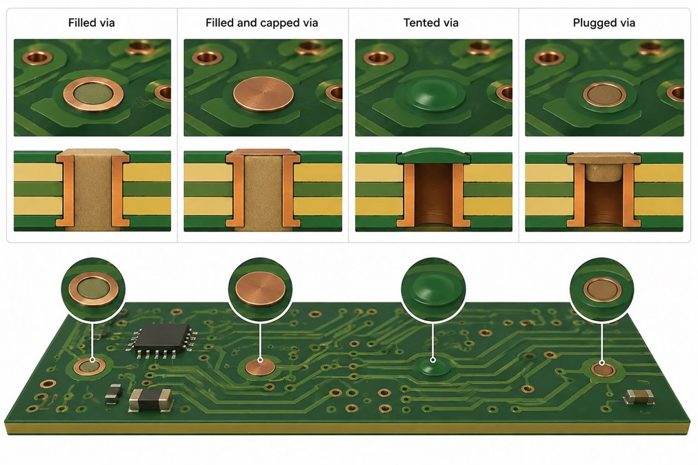
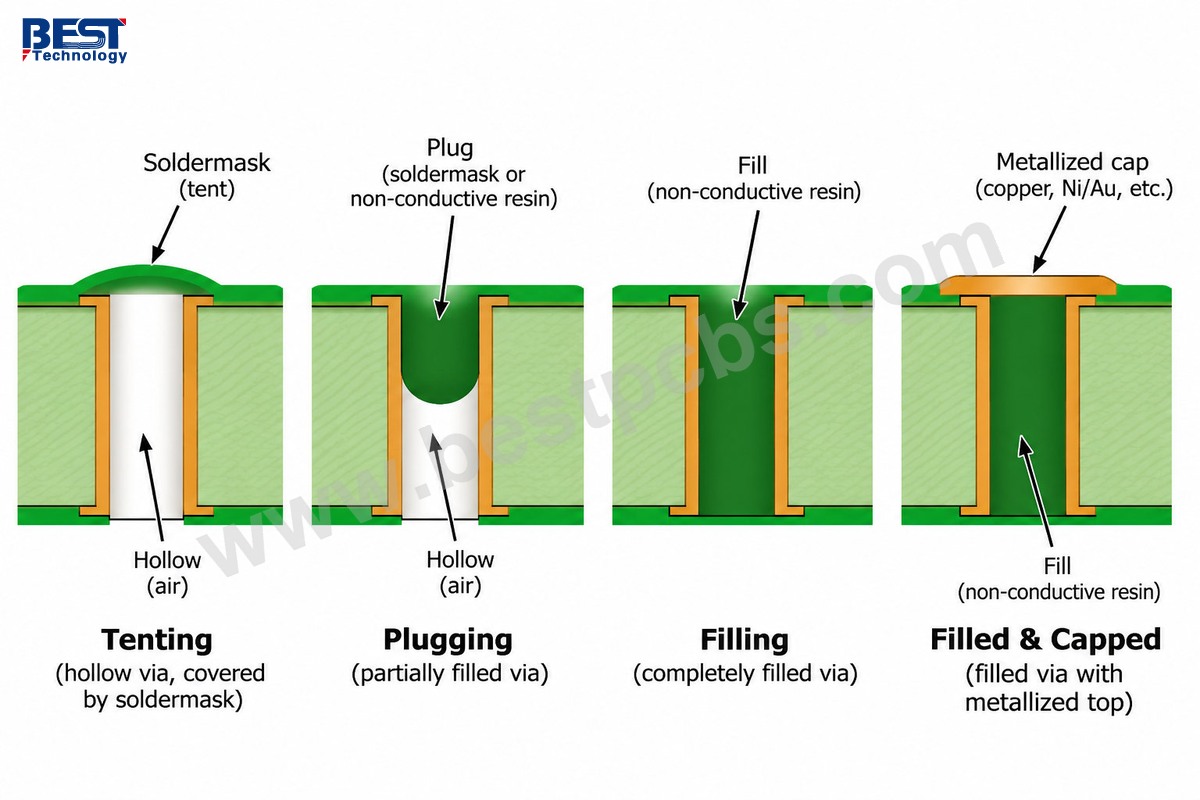
Via tenting covers the opening, plugging partially fills the barrel, and filling occupies the hole more completely. Each process offers a different level of internal protection, surface coverage, and suitability for PCB assembly.
| Process | Hole Condition | Typical Purpose |
|---|---|---|
| Tenting | Hollow | Surface protection |
| Plugging | Partially occupied | Partial hole closure |
| Filling | Filled barrel | Internal cavity filling |
| Filled and Capped | Filled, plated surface | Solderable via-in-pad |
1. Via Tenting
Tenting uses a protective mask across the hole entrance without intentionally introducing material through the barrel. It is commonly used for small signal vias where the main requirement is surface coverage. Manufacturing reliability depends on the opening diameter and selected mask process.
2. Via Plugging
Plugging introduces material partially into the via. The material, insertion depth, and curing requirements depend on the specified construction. Plugging provides partial hole closure, but it should not be described as full-barrel filling. Some designs also require a covering layer over the plugged opening.
3. Via Filling
Filling introduces suitable material throughout the via barrel. Common engineering concerns include:
- Fill material and compatibility.
- Internal voids.
- Curing and shrinkage.
- Surface recesses or protrusions.
- Additional covering requirements.
A filled via does not automatically have a continuous solderable copper surface.
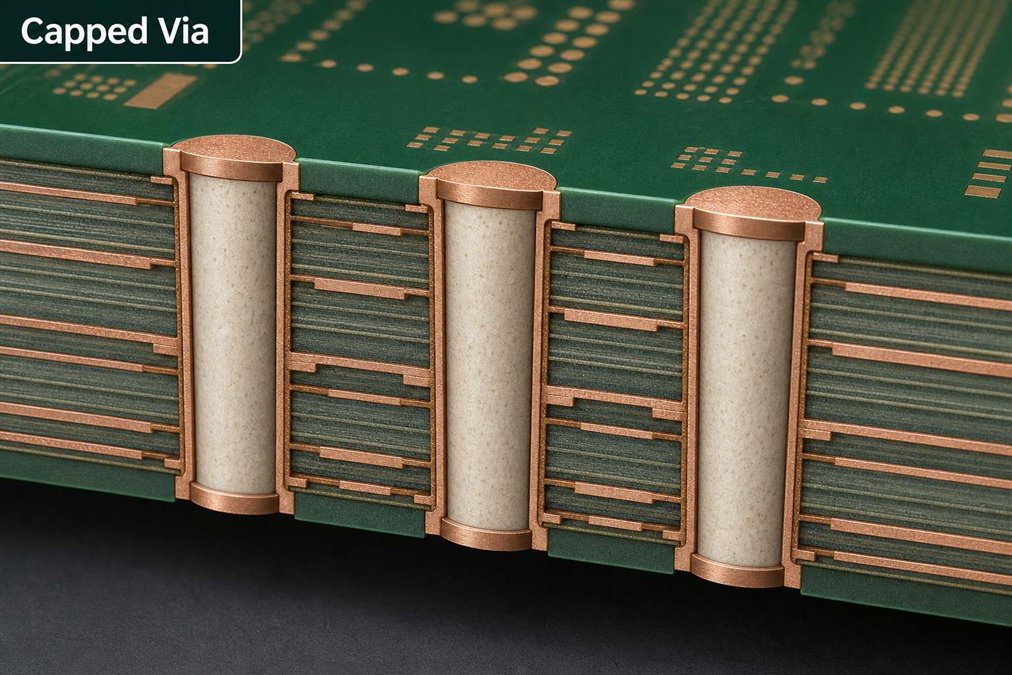
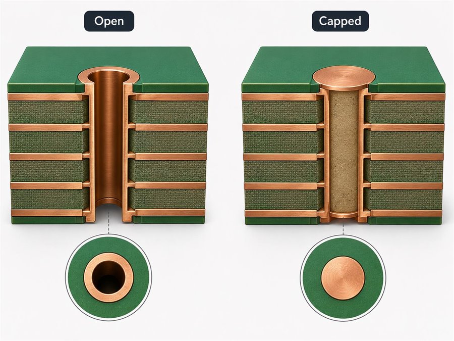
4. Filled and Capped Via
A filled and capped via combines internal filling with a metallized surface. For many conventional via-in-pad applications, the process includes filling, curing, planarization, and copper capping. This creates a more continuous solderable pad than ordinary tenting. The process is more demanding, but it is often selected when an SMT solder joint must form directly above the via.
What Via Size and Solder Mask Rules Are Required for Tenting?
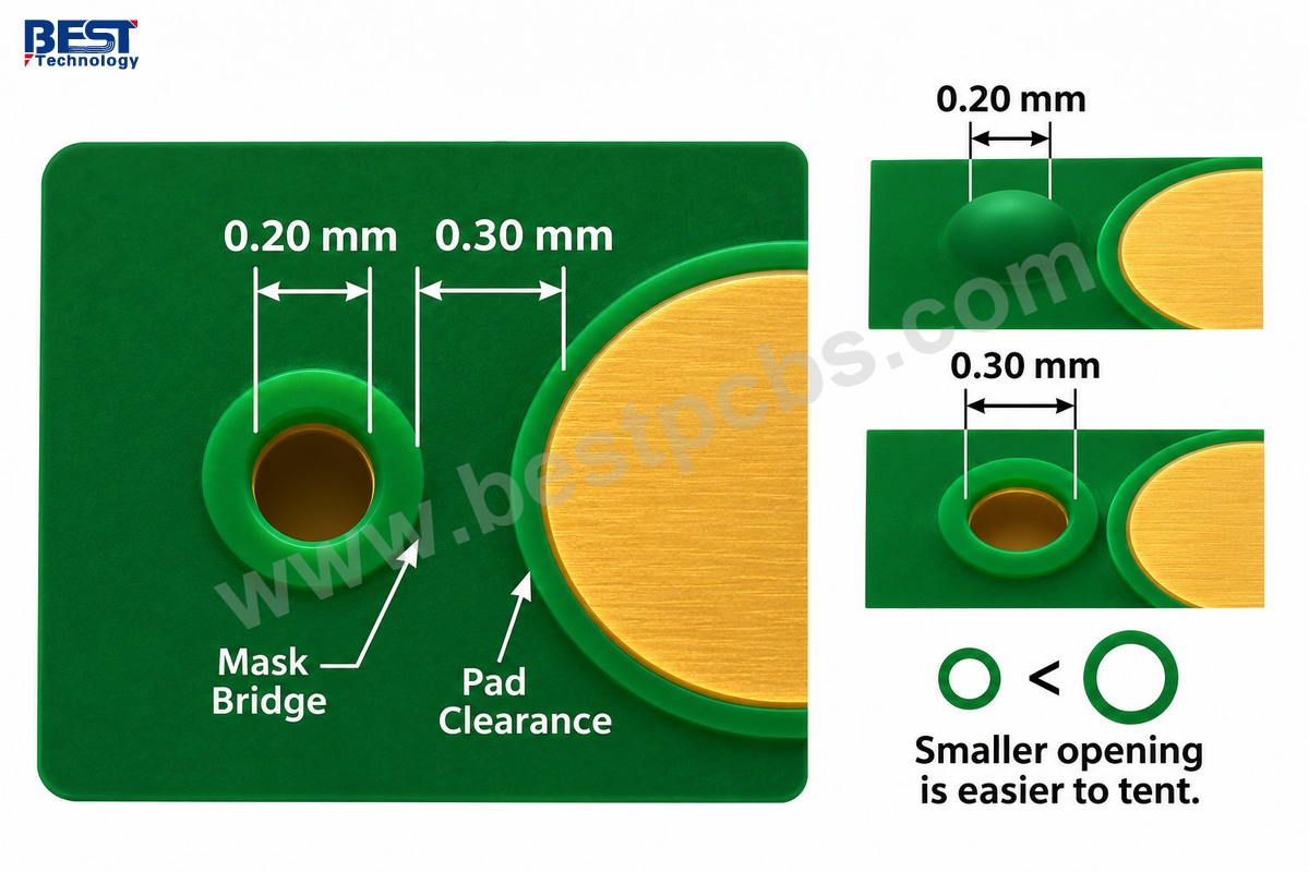
PCB via tenting depends on hole diameter, solder mask properties, annular ring geometry, and manufacturing capability. Openings around 0.30 mm or smaller are often considered suitable candidates, but IPC-4761 does not establish one universal maximum tenting diameter. The actual limit must be confirmed with the PCB manufacturer.
1. Via Drill Diameter
Smaller openings are generally easier to bridge with a continuous protective mask than larger openings.
| Nominal Hole Diameter | DFM Consideration |
|---|---|
| 0.20 mm | Common tenting candidate |
| 0.30 mm | Confirm coverage capability |
| 0.40 mm | Increased bridging difficulty |
| 0.50 mm | Consider alternative protection |
These dimensions are illustrative design references, not guaranteed EBest Circuit manufacturing limits. For example, a board containing both 0.20 mm and 0.40 mm vias may require different protection methods even when all vias use the same solder mask material.
2. Solder Mask Material and Thickness
Solder mask properties determine how consistently an opening can be covered. Important manufacturing parameters include:
- Material Type: Dry-film mask or LPI solder mask.
- Application Method: Lamination, coating, or printing.
- Coating Thickness: Influences bridging and mechanical strength.
- Curing Conditions: Affect mask integrity and adhesion.
- Surface Preparation: Supports adhesion to copper and laminate.
A solder mask process that reliably covers a small opening may produce incomplete coverage on a larger hole.
3. Annular Ring Width
The annular ring provides copper around the drilled via and supports connection between the barrel and surrounding circuitry. For example, consider a via pad diameter of 0.60 mm and a nominal hole diameter of 0.30 mm. The nominal radial annular ring is 0.15 mm, before drill-position and other manufacturing tolerances.
Copper annular ring dimensions and solder mask coverage must be reviewed separately. A suitable annular ring does not guarantee complete tenting.
4. Solder Mask Bridge and Pad Clearance
Vias close to SMT pads require enough spacing for a manufacturable solder mask bridge. Before releasing the design, confirm via-to-pad distance, solder mask expansion, minimum mask bridge width, mask registration tolerance, and required solderable pad opening. For example, a proposed 0.10 mm mask bridge should be checked against the manufacturer’s production capabilities.
The best design rule is the one confirmed for the selected PCB process, not a universal value copied from another manufacturer’s capability table.
What Are the IPC-4761 Via Protection Types?
IPC-4761 defines 7 principal via protection structures, from Type I tenting to Type VII filling and metal capping. These types describe how protective materials cover or occupy the hole, rather than the electrical connection structure of the via.
| IPC-4761 Type | Protection Structure |
|---|---|
| Type I | Tented |
| Type II | Tented and Covered |
| Type III | Plugged |
| Type IV | Plugged and Covered |
| Type V | Filled |
| Type VI | Filled and Covered |
| Type VII | Filled and Capped |
Type I — Tented
A dry-film mask bridges the via opening while leaving the barrel hollow. Type I-a describes one-sided protection, while Type I-b describes double-sided protection.
Type II — Tented and Covered
A tented structure receives an additional covering layer. Type II-a and Type II-b distinguish protection arrangements according to the covered surfaces.
Type III — Plugged
Plugging material partially occupies the via barrel. The material depth and application method depend on the specified construction.
Type IV — Plugged and Covered
The partially plugged via receives an additional protective covering. Both plug and cover requirements should be defined in the manufacturing specification.
Type V — Filled
The via barrel is filled with an approved material. The fill condition, void requirements, and resulting surface should be specified for the intended application.
Type VI — Filled and Covered
A filled barrel receives additional surface coverage. This provides a different construction from a via that is filled and subsequently copper capped.
Type VII — Filled and Capped
The filled hole receives a metallized cap. Type VII is commonly associated with via-in-pad structures that require a continuous solderable surface.
IPC-4761 is a design guide for via protection structures. It does not replace applicable PCB performance, workmanship, or acceptance requirements established through IPC-6012, IPC-A-600, and the approved purchasing documentation.
Can You Use Tented Vias Under BGA or Inside SMD Pads?
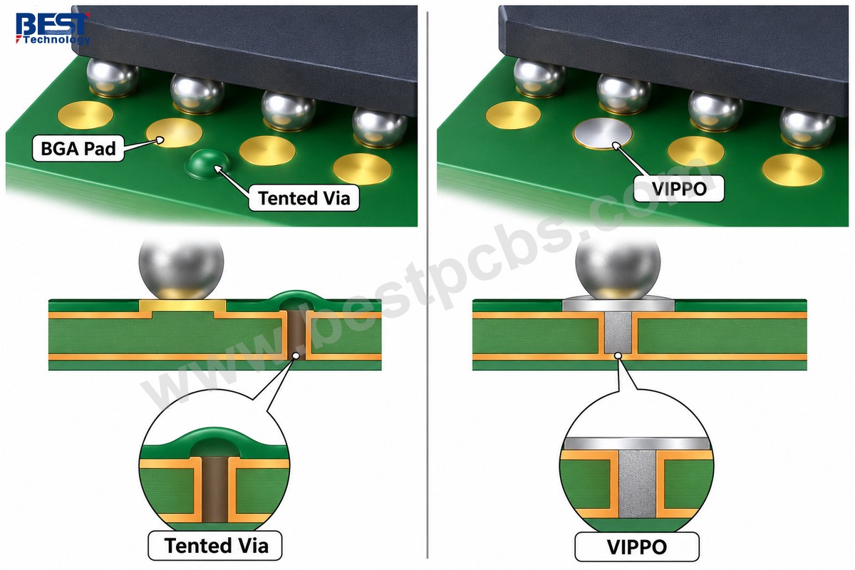
Tented vias may be suitable beneath BGA packages when they sit outside solderable pads, but conventional through vias directly inside solderable pads commonly require filling and capping. The main concerns are solder loss, pad flatness, and solder-joint formation.
1. Vias Near SMT Pads
A via beside an SMT pad can often be tented when adequate solder mask clearance is available. The fabricator should confirm that the mask can cover the opening while maintaining the intended solderable land and mask bridge.
2. Vias Under BGA Packages
BGA escape routing frequently places vias between fine-pitch pads. Tenting may be acceptable when:
- The via is outside the solderable land.
- The solder mask bridge is manufacturable.
- The protective layer does not interfere with assembly.
- The selected mask process provides suitable coverage.
The final decision depends on the BGA pitch, pad geometry, via dimensions, and manufacturing process.
3. Vias Directly Inside SMT Pads
An open via located within a solderable pad can draw molten solder into the barrel. Possible assembly problems include reduced solder volume, solder-joint voiding, uneven joints, inconsistent pad topography, and reduced assembly yield. For many conventional plated through-hole via-in-pad applications, a filled and capped construction provides a more appropriate solderable surface.
4. Tented Via vs VIPPO
| Feature | Tented Via | VIPPO |
|---|---|---|
| Barrel | Hollow | Filled |
| Surface | Solder mask | Metallized |
| Solderable Cap | No | Yes |
| Typical Use | Near SMT pads | Inside SMT pads |
| Relative Cost | Lower | Higher |
VIPPO means Via-in-Pad Plated Over. Its filled and plated structure helps maintain solderable pad continuity. The exact process depends on via geometry, component requirements, and selected manufacturing technology. For BGA designs, the critical requirement is a reliable solder joint—not simply a covered via opening.
How Do You Specify PCB Via Tenting in Gerber Files?
PCB via tenting should be defined through solder mask data, drill information, and fabrication notes. The files must identify which vias require coverage, which surfaces are protected, and whether a specific IPC-4761 construction is required.
1. Check Top and Bottom Solder Mask Layers
Gerber solder mask data typically defines where solder mask should be absent. For vias intended to remain covered, the corresponding mask openings are generally omitted from the relevant solder mask layer. Review top and bottom mask openings, CAD via protection settings, and exceptions for exposed vias and test points. The absence of a mask opening does not automatically guarantee complete closure over every hole size.
2. Identify the Required Protection Type
If the project requires a specific IPC-4761 type, include it in the fabrication drawing. For example, Type I-b indicates a double-sided dry-film tenting construction. A generic instruction such as tent all vias may suffice for an agreed standard solder mask process, but it is not a substitute for specifying a particular IPC construction.
3. Provide Complete Manufacturing Data
The PCB manufacturer should receive:
- Gerber or equivalent fabrication files.
- NC drill files.
- Top and bottom solder mask layers.
- Fabrication drawing.
- PCB revision and quantities.
- Required via protection specifications.
If different via groups require different treatments, identify them through a fabrication drawing, dedicated layer, coordinate list, or another agreed method.
4. PCB Via Tenting Fabrication Notes
Example A — Standard Solder Mask Coverage
Cover the designated non-test vias on both sides with solder mask according to the approved fabrication data. Confirm via diameter limits, coverage capability, and exceptions for solderable pads before production.
Example B — IPC-4761 Type I-b
Provide IPC-4761 Type I-b protection for the designated vias using the specified dry-film mask construction on both sides. Confirm material compatibility, hole dimensions, and inspection requirements before fabrication.
Use the second note only when Type I-b is the actual design requirement and the selected manufacturer supports the specified construction. For EBest Circuit projects, the fabrication drawing and Gerber data can be reviewed together during Free DFM.
What Are the Common PCB Via Tenting Defects and Reliability Risks?
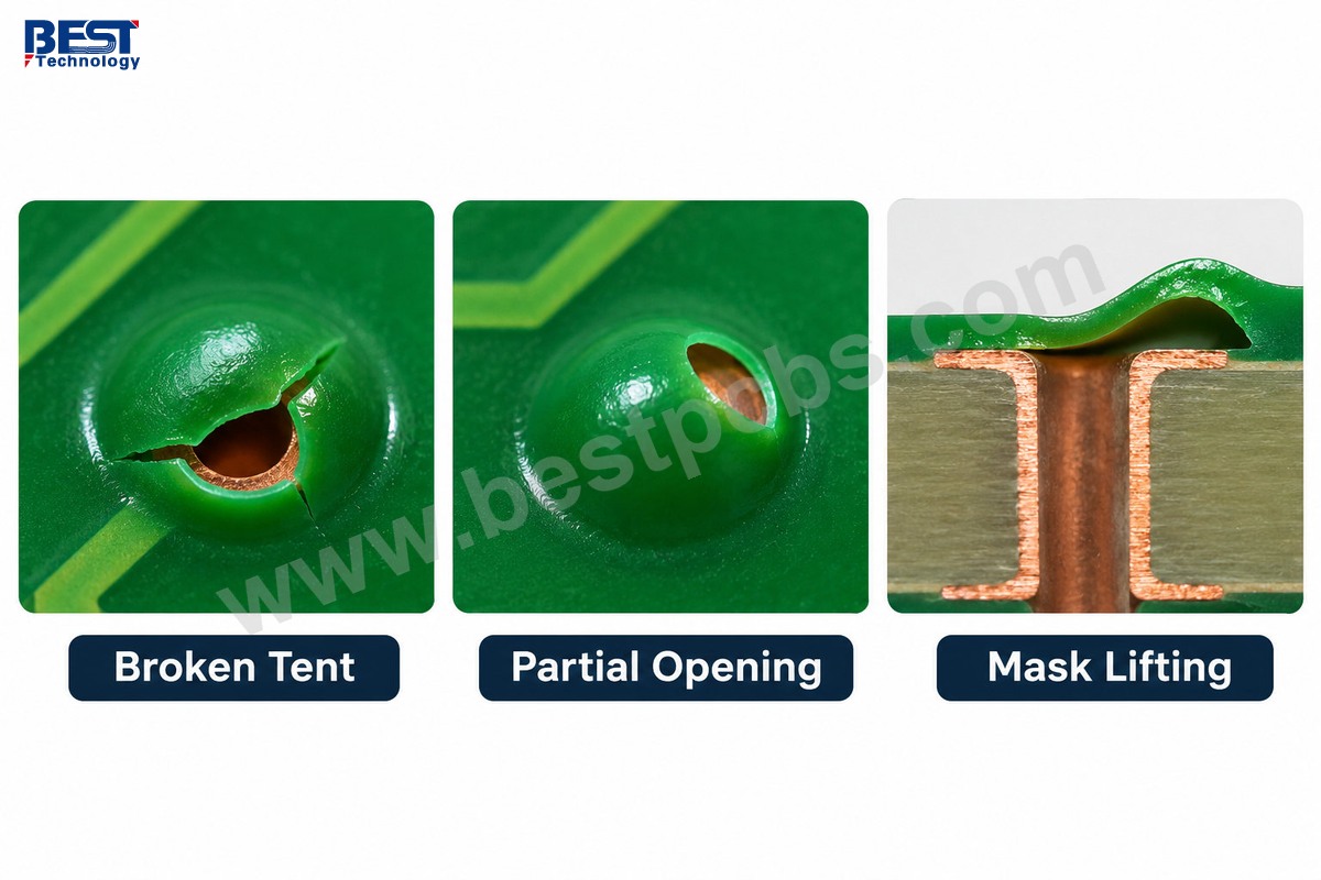
Common PCB via tenting defects include broken mask bridges, incomplete coverage, solder mask lifting, trapped residues, and surface irregularities. Their causes can involve hole geometry, material selection, cleaning, coating, curing, and later thermal processing.
| Defect | Possible Cause | Recommended Check |
|---|---|---|
| Broken Tent | Unsupported mask span | Hole size and mask |
| Partial Opening | Incomplete coverage | Application process |
| Mask Lifting | Adhesion issue | Surface preparation |
| Blistering | Trapped gas or residue | Cleaning and curing |
| Solder Wicking | Exposed opening | Mask integrity |
| Surface Bump | Excess material | Coating condition |
1. Broken Solder Mask Tent
A tent may crack when the protective layer cannot withstand process or handling conditions. Larger unsupported openings increase the difficulty of maintaining continuous coverage. The manufacturer should check hole dimensions, mask thickness, and material behavior.
2. Incomplete Coverage
Part of the via opening may remain exposed because the mask fails to bridge the full diameter. This is especially important near SMT pads, where exposed openings may affect solder paste behavior.
3. Trapped Processing Residues
Double-sided coverage can enclose the hollow barrel. If cleaning or processing residues remain inside, the enclosed materials may contribute to defects under certain conditions. Manufacturing sequence, cleaning, and curing should be considered when specifying protection on both sides.
4. Blistering and Mask Lifting
Blistering or poor adhesion can result from surface contamination, moisture or chemical residues, incomplete curing, material incompatibility, or thermal stress. A defect investigation should review the actual manufacturing history rather than automatically attributing the problem to solder mask quality.
5. Inspection Requirements
Depending on the project, inspection may include visual coverage checks, automated inspection, or cross-section analysis. A visibly covered via does not necessarily prove complete internal cleanliness or long-term reliability. Acceptance criteria should match the specified protection structure and end-use requirements.
How Do You Choose the Right Via Protection Process for PCB Manufacturing?
Choose tenting for suitable small vias needing surface protection, plugging for partial hole closure, filling for full-barrel treatment, and filled-and-capped construction where a continuous solderable pad is required. The decision should begin with the via’s function and location.
| PCB Requirement | Process to Evaluate |
|---|---|
| Ordinary small signal via | Tenting |
| Partial hole closure | Plugging |
| Full-barrel protection | Filling |
| Filled hole with surface mask | Filled and covered |
| Solderable via-in-pad | Filled and capped |
| Electrical test contact | Exposed conductive access |
1. Standard Signal Vias
Tenting is usually the first process to consider when the via is small, outside solderable pads, and does not need test access. The manufacturer should confirm reliable mask coverage for actual hole dimensions.
2. Dense SMT and BGA Areas
For vias near fine-pitch pads, mask registration and solder paste behavior take priority. If a reliable mask bridge cannot be maintained, plugging or another protection structure may be required.
3. Via-in-Pad Designs
For conventional mechanically drilled through vias located inside solderable pads, filling and capping are commonly considered to prevent solder loss and provide a continuous plated surface. The design should specify surface planarity and metallization requirements.
4. Thermal Vias
Thermal vias can connect component thermal pads to internal or opposite-side copper. Their treatment depends on solder paste behavior, thermal requirements, and assembly conditions. Open, tented, filled, or capped structures may be appropriate in different designs.
5. Cost-Sensitive PCB Production
Standard solder mask coverage is generally less complex than dedicated plugging, resin filling, planarization, and copper capping. However, choosing the lowest-cost treatment is useful only when it satisfies the electrical and assembly requirements. The preferred process is the least complex construction that reliably meets the design’s protection, soldering, and manufacturing needs.
Why Choose EBest Circuit for PCB Via Tenting and Manufacturing?
EBest Circuit provides PCB fabrication, via protection DFM reviews, and assembly support to help customers select manufacturable tenting, plugging, filling, and capped-via structures. Our engineering team reviews actual PCB dimensions and manufacturing requirements before recommending a suitable process.
Our services include:
- Free DFM Review: Examine drill sizes, annular rings, mask openings, via-to-pad spacing, and protection requirements.
- Via Protection Engineering: Review whether tenting, plugging, filling, or capping is suitable for the intended PCB construction.
- PCB Manufacturing: Support FR4, multilayer, HDI, and other PCB fabrication projects.
- No MOQ: Support engineering prototypes and small production quantities.
- PCB Assembly Coordination: Review via treatment alongside SMT, BGA, and through-hole assembly requirements.
- Manufacturing Quality Control: Establish project-specific inspection requirements for solder mask coverage and via construction.
- Engineering Support: 1 sales representative and 3 engineers coordinate technical reviews and production communication.
Our manufacturing operations are supported by applicable quality management certifications, including ISO 9001, ISO 13485, IATF 16949, and AS9100D, with certification scope available for supplier qualification.
For PCB via tenting, solder mask plugging, resin filling, or via-in-pad projects, send your Gerber files, drill files, solder mask layers, fabrication drawings, quantities, and IPC-4761 requirements to sales@bestpcbs.com. Our engineers can review your design and provide a project-specific manufacturing quotation.
Frequently Asked Questions About PCB Via Tenting
1. Is via tenting required for every PCB?
No. Via tenting is selected according to layout and assembly requirements. Small signal vias are common candidates, while test points need accessible conductive surfaces. Vias inside solderable component pads may require filled-and-capped structures rather than ordinary tenting.
2. Can solder mask reliably cover a 0.3 mm via?
Yes, a 0.30 mm opening can be tented using a suitable process, but reliable coverage must be confirmed with the PCB manufacturer. Mask material, thickness, application method, and hole geometry affect the result. A commonly cited diameter is not a universal manufacturing guarantee.
3. Does via tenting completely seal the hole?
Not necessarily. Via tenting covers the opening while leaving the internal barrel hollow. It can reduce exposure to solder and contaminants, but the resulting structure should not automatically be treated as hermetically sealed or equivalent to a fully filled via.
4. Can a tented via be used as a test point?
A fully tented via is generally unsuitable for direct electrical probing because the solder mask covers the conductive surface. If a via must serve as a test point, the design should provide exposed copper with an appropriate surface finish and sufficient probe access.
5. Can via tenting cause trapped air or moisture?
Yes, double-sided coverage can create conditions where moisture, gases, or process residues remain inside a hollow via. Whether these cause a defect depends on cleaning, curing, material selection, and operating conditions. The manufacturer should review protection structure and process sequence.
6. Is double-sided via tenting better than single-sided tenting?
Not always. Double-sided tenting provides coverage on both PCB surfaces, while single-sided tenting leaves one opening exposed. The preferred choice depends on soldering, surface protection, processing residues, and manufacturing requirements rather than the number of covered sides alone.
7. Does via tenting increase PCB manufacturing cost?
Standard solder mask coverage may add little or no separate cost when included in the normal process. Dedicated dry-film tenting, plugging, resin filling, planarization, and copper capping can require additional manufacturing steps. Actual pricing depends on specified structure, hole dimensions, board quantity, and production process.
Conclusion
PCB via tenting protects suitable plated vias by covering their openings while leaving the barrels hollow. Reliable results depend on via dimensions, solder mask capability, pad location, and manufacturing controls. IPC-4761 helps distinguish tented, plugged, filled, and capped structures, while BGA and via-in-pad designs require particular attention to solderability and surface planarity. EBest Circuit supports these requirements through Free DFM, PCB fabrication, No MOQ, and engineering assistance. Send your Gerber files, drill data, and via protection specifications to sales@bestpcbs.com for a manufacturing review and quotation.