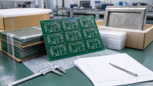
PCB fast prototyping helps engineers move a new board from design files to a real, testable sample before committing to larger production. It is useful when a project needs to verify fit, routing, material selection, surface finish, soldering quality, component sourcing, assembly process, and early functional performance.
EBest Circuit (Best Technology) supports PCB fast prototyping, DFM review, PCB fabrication, component sourcing, SMT assembly, testing coordination, and small-batch production. If your project is ready for prototype review, send your Gerber files, BOM, drawing, stackup notes, impedance requirements, or assembly files to sales@bestpcbs.com. Our engineering team can help better check the manufacturing path before production starts.
How PCB Fast Prototyping Helps Validate a New Board
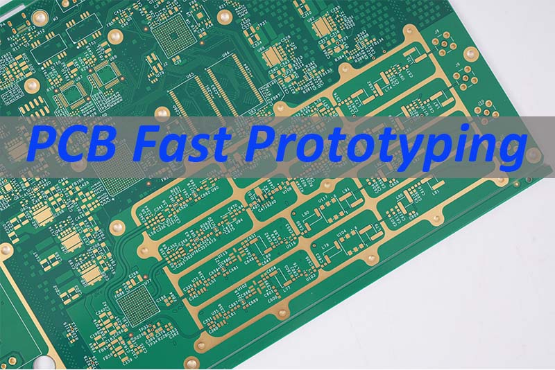
PCB fast prototyping is not only about making a board quickly. The real value is helping engineers find practical problems early.
A prototype can help verify:
| Validation Point | What Engineers Can Check |
|---|---|
| Board structure | Thickness, outline, holes, slots, panelization |
| Materials | FR4, Tg value, copper weight, solder mask, surface finish |
| Assembly fit | Connector position, component clearance, SMT feasibility |
| Manufacturing risk | Minimum trace, spacing, drilling, plating, solder mask bridge |
| Production path | Whether the sample can move into small batch or mass production |
For a simple FR4 PCB, the prototype may mainly confirm mechanical size and soldering quality. For HDI, impedance, flexible PCB, rigid-flex PCB, metal core PCB, or PCBA projects, fast prototyping becomes much more important because the first build can reveal stackup, fabrication, assembly, and testing risks.
A good fast prototype should not be treated as a one-time sample. It should be built in a way that makes the next production step easier.
EBest Circuit PCB Fast Prototyping Lead Time
PCB fast prototyping lead time should be checked by board type, layer count, standard specification, and whether the project includes SMT assembly. A simple FR4 prototype can move much faster than an HDI board, ceramic PCB, rigid-flex PCB, or PCBA project with component sourcing.
For standard FR4 prototypes under 1 square meter, EBest Circuit can use the following lead time range as a practical reference:
| FR4 Prototype | Normal Service | Fastest Service |
|---|---|---|
| 1 layer | 7 days | 24 hours |
| 2 layers | 8 days | 24 hours |
| 4 layers | 10 days | 48 hours |
| 6 layers | 10 days | 72 hours |
| 8 layers | 12 days | 72 hours |
| 10+ layers | To be confirmed | To be confirmed |
This reference is based on standard FR4 prototype conditions, such as 0.4-1.6mm board thickness, H/H or 1oz copper, lead-free HASL, green solder mask, white silkscreen, minimum line width/space above 8 mil, minimum hole above 0.3mm, and minimum annular ring above 10 mil.
For other prototype types, the lead time needs separate review:
| Prototype Type | Practical Lead Time Reference |
| 1-layer MCPCB | Normal about 4 days; urgent service can be discussed |
| 2-layer MCPCB | Longer than standard FR4 because of metal core processing |
| Rigid-flex PCB | About 2 weeks for common 4-layer projects; complex builds need review |
| Ceramic PCB | Usually longer because of substrate and process requirements |
| PCBA prototype | Depends on PCB, BOM sourcing, stencil, SMT, inspection, and packing |
The fastest schedule is only realistic after the files are confirmed. If the board has special laminate, tight impedance, HDI microvias, heavy copper, black solder mask, fine-pitch SMT, special packing, or customer-approved production files, EBest Circuit will check these details before confirming the final delivery date.
For increasingly urgent projects, the best way is to send the Gerber files, BOM, drawings, stackup notes, and assembly files early, so the engineering and production teams can confirm whether the project fits fast service or needs a safer prototype schedule.
Fast Prototype PCB vs Standard PCB Production
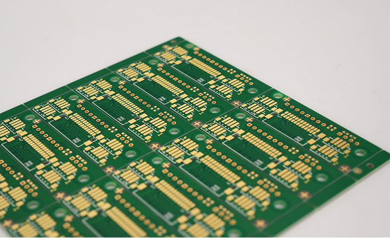
A fast prototype PCB and standard PCB production have different goals.
| Item | Fast Prototype PCB | Standard Production |
|---|---|---|
| Main goal | Verify the board quickly | Build repeatable batches |
| Quantity | Sample or small batch | Stable batch quantity |
| Review focus | DFM risks and urgent feasibility | Yield, cost, process control |
| Panelization | May be flexible | Usually optimized for production |
| Documentation | Basic to project-specific | More complete production records |
Fast prototyping is best when engineers need quick feedback. Standard production is better when the design has already passed validation and the focus moves to cost, consistency, quality reports, and repeat delivery.
For many projects, the best path is:
Prototype first, review the result, adjust if needed, then move into small-batch or mass production.
PCB Fast Prototyping Capabilities at EBest Circuit
EBest Circuit supports PCB fast prototyping for standard FR4 boards, multilayer PCBs, HDI PCBs, metal core PCBs, ceramic PCBs, flexible PCBs, rigid-flex PCBs, and PCBA prototypes. For customers, the key is not only whether the board can be made quickly, but whether the prototype can be reviewed, built, assembled, tested, and prepared for the next production step.
For standard FR4 prototype projects, common fast-build conditions include:
| Item | Reference Capability |
|---|---|
| Board thickness | 0.4-1.6mm |
| Copper | H/H or 1oz |
| Surface finish | Lead-free HASL |
| Solder mask | Green |
| Silkscreen | White |
| Min line/space | >8 mil |
| Min hole | >0.3mm |
| Min annular ring | >10 mil |
For projects beyond standard FR4, EBest Circuit can review more advanced requirements:
| Area | Examples |
|---|---|
| Materials | High Tg FR4, halogen-free FR4, selected RF materials |
| Structures | Multilayer, HDI, blind/buried vias |
| Thermal boards | MCPCB, ceramic PCB |
| Assembly | Component sourcing, SMT, inspection |
| Reports | Electrical test, impedance, inspection reports |
These capabilities do not mean every project can use the same urgent schedule. A simple 2-layer FR4 sample may fit fast service, while an HDI board, heavy copper board, ceramic PCB, rigid-flex PCB, or full PCBA prototype needs engineering review before the lead time is confirmed.
Before production, EBest Circuit early reviews the Gerber files, drill file, stackup, board thickness, copper thickness, surface finish, impedance notes, BOM, pick-and-place file, and packing requirements. This helps customers much more easily avoid a common problem: receiving a fast sample that cannot smoothly move into assembly or small-batch production.
Fast Turn PCB Prototype Process Step by Step
A fast turn PCB prototype needs a clear process. Speed is useful only when the project details are strictly controlled.
A typical EBest Circuit process includes:
- File review
Gerber files, drill files, drawings, stackup notes, and assembly files are checked. - DFM check
Engineers review manufacturability risks such as spacing, holes, solder mask, copper, outline, and panelization. - Quotation and lead time confirmation
The final price and schedule are confirmed based on board complexity and quantity. - Production data confirmation
For special projects, production files or stackup details can be sent to the customer for confirmation before manufacturing. - PCB fabrication
The board enters material preparation, imaging, etching, drilling, plating, solder mask, surface finish, profiling, and test. - SMT assembly if required
For PCBA prototypes, components are sourced or received, then assembled and inspected. - Final inspection and shipment
Boards are checked, packed, and shipped according to project requirements.
This process keeps the prototype fast, but still controlled.
PCB Material and Surface Finish Options for Fast Prototyping
PCB material and surface finish should match the product use, not only the fastest delivery option.
Common fast prototype options include:
| Option | Typical Use |
|---|---|
| FR4 Tg130 | Standard electronics and general prototypes |
| FR4 Tg150 / Tg170 | Higher heat or reliability requirements |
| 1oz copper | Common signal and control boards |
| 2oz copper | Higher current or thermal needs |
| HASL lead-free | Cost-sensitive prototypes |
| ENIG | Fine pitch, flat surface, better solderability |
| Green solder mask | Standard production choice |
| Black, white, blue, red mask | Appearance or product matching |
For urgent projects, material availability can affect lead time. If a project uses special laminate, heavy copper, high Tg FR4, controlled impedance, HDI structure, FPC material, or special surface finish, the fastest realistic schedule should be confirmed after engineering review.
Fast Flexible PCB Prototyping and Rigid-Flex Prototype Support
Fast flexible PCB prototyping is useful for compact devices, wearable electronics, sensors, camera modules, connectors, medical electronics, and products with limited internal space.
Flexible and rigid-flex prototypes require more attention than standard rigid PCBs because the board may include:
| Area | What Needs Review |
|---|---|
| Flexible area | Bend direction and dynamic or static use |
| Coverlay | Opening size and adhesive control |
| Stiffener | Connector or soldering support |
| Material | PI, copper type, thickness |
| Rigid-flex transition | Stress and manufacturing reliability |
| Assembly | SMT support and handling protection |
EBest Circuit can support flexible PCB and rigid-flex PCB prototype review based on customer-provided design files and product requirements. For these boards, fast delivery must be balanced with material selection, process reliability, and production yield.
PCB Fast Prototyping Case Study
One fast prototype project involved a 4-layer FR4 PCB that needed both bare PCB fabrication and SMT assembly support.
Project background
The customer needed a prototype build for product validation before moving toward a more stable production plan. The project was not only a bare PCB order because EBest Circuit also handled component purchasing and SMT assembly.
Key board requirements
| Item | Requirement |
|---|---|
| Board type | 4-layer FR4 PCB |
| Material | FR4 Tg130 |
| Finished thickness | 1.6mm ±10% |
| Copper thickness | 1oz / 1oz / 1oz / 1oz |
| Solder mask | Black |
| Silkscreen | White |
| Surface finish | Lead-free HASL |
| Panelization | Factory panelization allowed |
| Components | Purchased by EBest Circuit |
| Delivery | Single-unit delivery after SMT |
Main project focus
This prototype had three practical concerns.
- First, the board needed a stable 4-layer FR4 manufacturing path. The engineering team checked the thickness, copper structure, solder mask, surface finish, and panelization method before production.
- Second, the project required SMT support. Since all components were purchased by EBest Circuit, BOM review and sourcing coordination were part of the prototype schedule. This helped the customer avoid managing PCB fabrication and component purchasing separately.
- Third, the customer requested single-unit delivery after SMT. That meant packing and handling needed to match the assembled board condition, not only the bare PCB condition.
For the customer, the value was not just a fast prototype PCB. The value was a complete prototype path: DFM review, PCB fabrication, component sourcing, SMT assembly, inspection, and delivery in one workflow.
Why Choose EBest Circuit for PCB Fast Prototyping?
EBest Circuit is suitable for customers who need more than a simple online prototype order.
Our support includes:
| EBest Circuit Support | Customer Value |
|---|---|
| DFM pre-review | Find risks before production |
| Engineering support | Review PCB and PCBA manufacturing details |
| PCB + PCBA factory | Reduce handoff between suppliers |
| Component sourcing | Support approved BOM purchasing |
| SMT assembly | Build functional prototype boards |
| Prototype and small batch | Support R&D validation and early production |
| Quality certifications | ISO9001, ISO13485, IATF16949, AS9100D |
| Digital traceability | Track material, batch, cycle, and production status |
For engineers, the best PCB fast prototyping supplier is not always the one that promises the shortest time. It is the one that can tell which parts of the project are simple, which parts need engineering review, and which risks should be solved before the board moves into production.
EBest Circuit supports prototype-to-production projects for customers who need custom PCB fabrication, component sourcing, PCBA assembly, and practical manufacturing support.
PCB Fast Prototyping FAQs
1. What is the difference between PCB fast prototyping and normal PCB prototyping?
PCB fast prototyping focuses on shorter lead time for engineering validation. Normal PCB prototyping may follow a standard schedule, especially when the board has special material, HDI, impedance, flexible PCB, or assembly requirements.
2. Can fast PCB prototyping include SMT assembly?
Yes. A fast PCB prototype can include SMT assembly if the BOM, placement file, Gerber files, and assembly notes are complete. The lead time must include component sourcing or component receiving, stencil preparation, SMT, inspection, and packing.
3. Is lead-free HASL suitable for fast prototype PCB projects?
Lead-free HASL can be suitable for many standard FR4 prototype boards. If the board has fine-pitch components, BGA, or very flat pad requirements, ENIG may be a better option.
4. Can EBest Circuit support fast flexible PCB prototyping?
Yes. EBest Circuit supports flexible PCB and rigid-flex PCB prototype projects. The lead time depends on material, stackup, coverlay, stiffener, surface finish, and inspection requirements.
5. What files should I send for PCB fast prototyping?
Please send Gerber files, drill files, board drawing, stackup notes, BOM, pick-and-place file, assembly drawing, impedance notes, and any special requirements such as thickness tolerance, surface finish, panelization, testing, or packing.
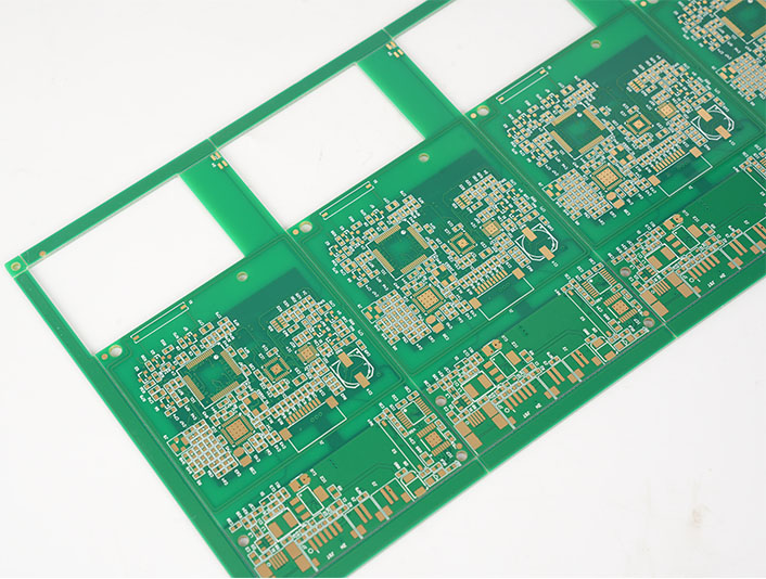
In short, a fast prototype should help you move forward, not create more uncertainty. If you are preparing a new PCB or PCBA project, send your Gerber files, BOM, drawings, stackup notes, impedance requirements, or assembly files to sales@bestpcbs.com. EBest Circuit will help review the manufacturing path and support your project from prototype validation to scalable production.