PCB manufacturing PCB manufacturing
Home > Blog

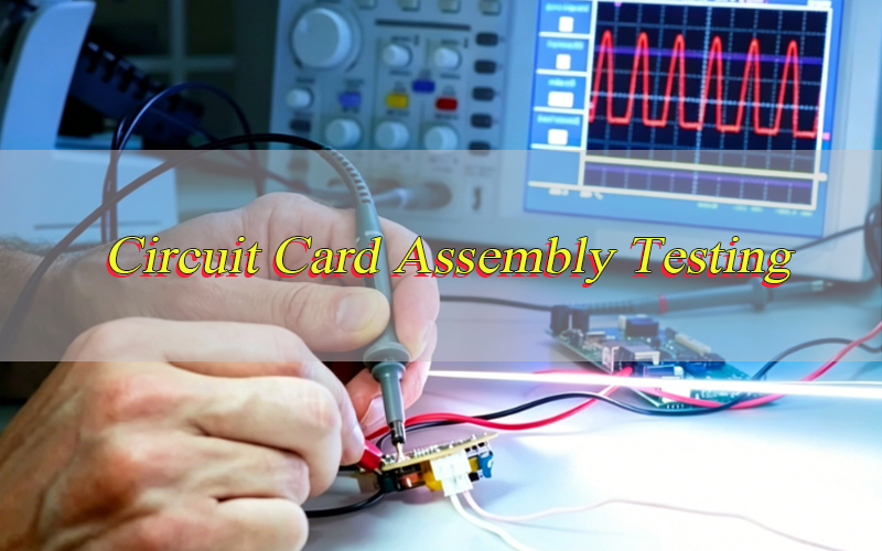
Which Circuit Card Assembly Testing Methods Fit Your Manufacturing Needs?

May 6th, 2026

If your manufacturing line relies on consistent, reliable circuit card assemblies, how do you ensure each unit meets the standards your operations demand? How do you leverage circuit card assembly testing to choose the right approach and avoid costly rework, delays, and product failures?

Circuit card assembly testing is essential for consistent production, and navigating its many methods, equipment and requirements can be overwhelming. This guide helps you choose the right testing methods for your manufacturing needs, detect defects early, and maintain high-quality output.

Circuit Card Assembly Testing, https://www.bestpcbs.com/blog/2026/05/circuit-card-assembly-testing-2/

What Is Circuit Card Assembly Testing and How Does It Work?

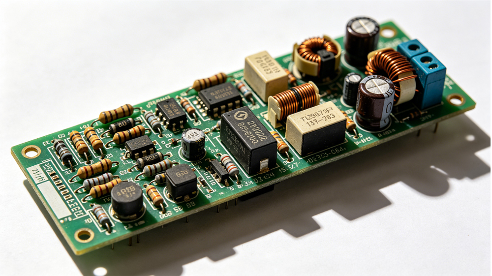
Circuit card assembly testing is a straightforward process designed to confirm that assembled circuit boards work as they should. It ensures each board meets the design requirements set for it and is free of any defects that could affect its performance or how long it lasts. Without this testing, even small issues can lead to bigger problems down the line, from product failures to wasted time and money.

At its core, this testing checks two key things: the physical condition of the assembly and its electrical functionality. It verifies that every component, from resistors and capacitors to solder joints and connections, is in the right place and working properly. This dual check helps catch both obvious surface issues and hidden problems that might not be visible to the naked eye.

The process itself is simple: controlled inputs are applied to the circuit card, and the outputs are measured and compared to predefined standards. Depending on the needs of the production run, testing methods can vary; some are automated for fast, high-volume testing, while others are more flexible for small batches or prototypes. The end goal is always the same: to catch issues early and ensure consistent, reliable quality.

Why Is Circuit Card Assembly Testing Critical for Product Quality and Reliability?

Circuit card assembly testing is critical for product quality and reliability. It safeguards electronic product performance and longevity, catches defects early to avoid faulty units, reduce rework costs and delays, ensures design compliance, and enhances long-term reliability while protecting brand trust.

  • Prevents Defective Products from Reaching Customers Unchecked defects in circuit card assemblies can lead to product failures, customer complaints, and reputational damage. Testing ensures only fully functional units leave the manufacturing line, protecting brand trust and reducing returns.
  • Reduces Rework and Production Costs Catching defects early in the manufacturing process is far less expensive than fixing them after assembly or after delivery. Testing eliminates the need for costly rework, scrap, and replacement parts, improving overall production efficiency.
  • Ensures Compliance with Design Specifications Circuit card assemblies must meet strict design requirements to work with other system components. Testing verifies that each assembly aligns with electrical, mechanical, and performance standards, preventing compatibility issues.
  • Enhances Long-Term Reliability Defects like poor solder joints or component misalignment may not cause immediate failure but can lead to premature breakdowns in the field. Testing identifies these hidden issues, ensuring assemblies perform consistently over their intended lifespan.
  • Minimizes Production Delays Unplanned rework or product recalls due to untested defects can halt production lines and delay deliveries. Consistent testing streamlines the manufacturing process, keeping operations on schedule and meeting customer deadlines.

What Are the Main Types of Circuit Card Assembly Testing Methods Available?

Choosing the right circuit card assembly testing method depends on factors like production volume, assembly complexity, and testing goals. Each method has unique strengths, designed to address specific testing needs from fast, automated checks for high-volume runs to flexible, fixtureless options for prototypes and complex assemblies. Below is a breakdown of the most common methods, their key features, and ideal use cases.

  • In-Circuit Testing (ICT) A popular method for high-volume production, ICT uses a bed-of-nails fixture to test individual components and connections on the circuit card assembly. It checks for component values, solder shorts, open circuits, and incorrect part placements. This method delivers fast, accurate results for mass-produced units.
  • Flying Probe Testing A flexible, fixtureless method ideal for low-volume production, prototypes, or complex assemblies. Flying probe testers use movable probes to access test points, eliminating the need for custom fixtures. This approach works well for quick turnaround and design iterations.
  • Functional Testing Verifies that the entire circuit card assembly operates as intended in real-world conditions. It applies inputs similar to those the assembly will encounter in use and measures outputs to ensure performance meets design standards. This type of testing is critical for validating end-to-end functionality.
  • Automated Optical Inspection (AOI) Uses high-resolution cameras and image analysis to check the physical appearance of the circuit card assembly. It detects surface defects like missing components, misaligned parts, solder bridging, and poor solder joints. AOI is often used as a first-pass test in production.
  • X-Ray Inspection Used for hidden defects that are invisible to the naked eye or AOI. Examples include internal solder joints in ball grid arrays (BGAs) or quad flat packages (QFPs). X-ray testing penetrates the assembly to check for voids, cold solder joints, and component misalignment.
Circuit Card Assembly Testing, https://www.bestpcbs.com/blog/2026/05/circuit-card-assembly-testing-2/

How Do Flying Probe Testing and In-Circuit Testing Differ in Circuit Card Assembly Testing?

FeatureFlying Probe TestingIn-Circuit Testing
Fixture RequirementNo custom fixture needed; uses movable probes to access test pointsRequires a custom bed-of-nails fixture tailored to the specific circuit card assembly
Production Volume SuitabilityIdeal for low-volume production, prototypes, and design iterationsOptimized for high-volume production, where fixture costs are offset by fast testing speeds
Testing SpeedSlower than ICT, as probes move to each test point individuallyFast, with simultaneous testing of multiple points via the bed-of-nails fixture
Complexity HandlingExcels with complex assemblies, fine-pitch components, and tight test point spacingMay struggle with very complex assemblies or limited test point access
CostLower upfront costs (no fixture), but higher per-unit testing costs for high volumesHigher upfront costs (fixture design and fabrication), but lower per-unit costs for high volumes
Turnaround TimeFast setup with no fixture, ideal for quick prototyping and small batchesLonger setup time due to fixture design and installation, better for consistent high-volume runs

What Common Defects Can Circuit Card Assembly Testing Detect?

Circuit card assembly testing plays a vital role in identifying a range of common defects that can arise during manufacturing, from visible surface issues to hidden flaws that may cause premature failure. These defects, which can stem from soldering mishaps, component placement errors, or material issues, can compromise the assembly’s functionality if left undetected. Below is a detailed breakdown of the most frequent defects and how testing methods uncover them.

  • Open Circuits: Breaks in the circuit path that prevent electrical current from flowing. These are often caused by poor solder joints, broken traces, or component lead issues. Continuity tests in ICT, flying probe testing, or functional testing can detect them.
  • Solder Shorts: Unintended electrical connections between two or more circuit points. These are typically caused by excess solder or solder bridging. AOI and X-ray testing are effective for identifying surface and hidden solder shorts.
  • Missing Components: Components that are not placed on the circuit card assembly during manufacturing. AOI and visual inspection (manual or automated) quickly detect missing resistors, capacitors, integrated circuits, and other parts.
  • Misplaced Components: Components placed in the wrong location or orientation, which can render the assembly nonfunctional. AOI and ICT verify component placement against design specifications.
  • Incorrect Component Values: Components with values that do not match the design. An example is a 1k resistor instead of a 10k resistor. ICT and functional testing measure component values to ensure accuracy.
  • Cold Solder Joints: Solder joints that do not form a proper bond with the component lead and circuit pad. These can lead to intermittent connections or complete failure. X-ray testing and functional testing can detect these hidden defects.
  • Component Damage: Physical damage to components such as cracked chips or bent leads. It also includes damage from electrostatic discharge (ESD) during manufacturing. AOI and visual inspection identify visible damage, while functional testing uncovers performance issues from hidden damage.

When Should You Perform Circuit Card Assembly Testing in the Manufacturing Process?

Circuit card assembly testing must be timed strategically throughout the manufacturing process to maximize effectiveness and minimize costs. The right testing timing ensures defects are caught early, rework is reduced, and final products meet quality standards. Below is a breakdown of key stages to perform testing, aligned with production workflows to keep operations efficient and reliable.
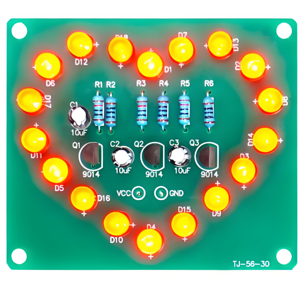
  • After Component Placement and Soldering: The first critical testing point is immediately after components are placed and soldered. This step catches surface-level defects like missing components, misplacement, and solder shorts early. It prevents additional assembly steps from increasing rework costs.
  • After Rework or Repair: Any time a circuit card assembly is reworked or repaired, testing is essential. It ensures the repair was successful and no new defects were introduced. This prevents faulty repaired units from moving forward in production.
  • Before Final Assembly: Testing before the circuit card assembly is integrated into the final product ensures it functions correctly with other system components. This step avoids costly disassembly if the assembly is defective.
  • Before Shipping: A final test before shipping confirms that the circuit card assembly meets all performance and quality standards. This is the last line of defense against defective products reaching customers.
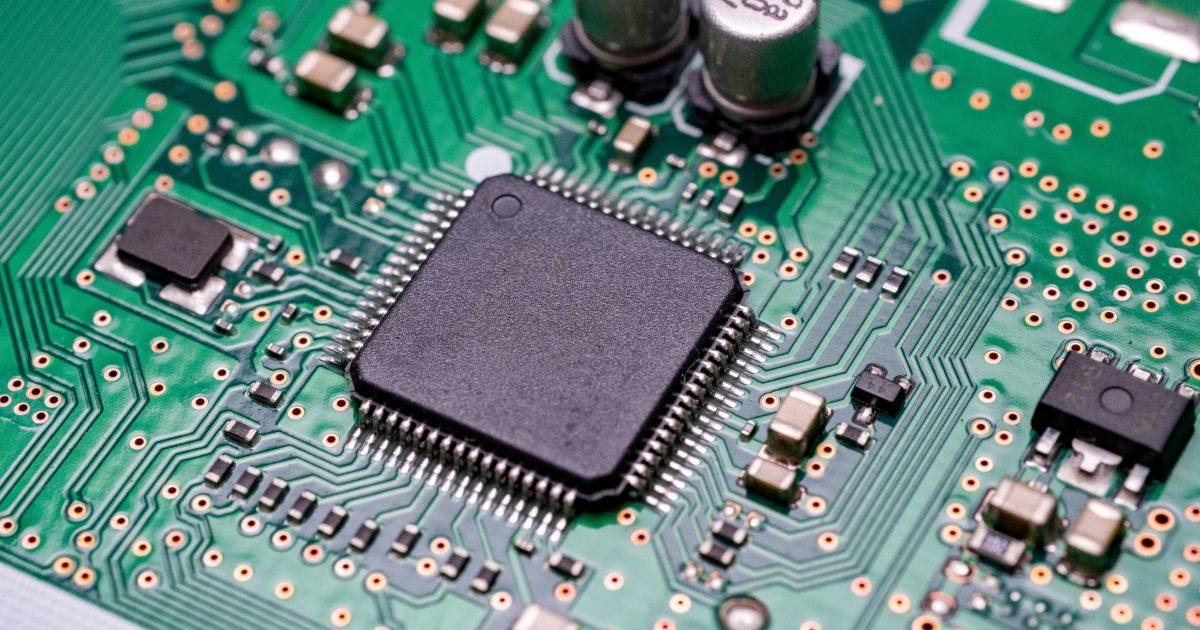
  • During Prototype Development: Testing during prototype development helps validate the design. It identifies potential issues and allows for adjustments before mass production. This reduces the risk of costly design changes later in the process.

What Equipment Is Needed for Effective Circuit Card Assembly Testing?

Effective circuit card assembly testing relies on the right tools and equipment, tailored to your testing methods and production needs. The right equipment ensures accurate, efficient defect detection, whether for high-volume automated testing or flexible low-volume checks. Below is a breakdown of essential equipment and its role in reliable testing processes.

  • In-Circuit Test Fixtures: Custom bed-of-nails fixtures designed to match the test points of the specific circuit card assembly. These fixtures connect the assembly to the ICT machine for fast, automated testing.
  • Flying Probe Testers: Automated machines with movable probes that access test points without a custom fixture. They include high-precision motors and sensors to ensure accurate probe placement.
  • AOI Machines: High-resolution cameras, lighting systems, and image analysis software to detect physical defects. Advanced models include 3D capabilities for better detection of solder joint issues.
  • X-Ray Inspection Systems: X-ray sources and detectors to visualize internal components and solder joints. These systems are essential for testing BGAs, QFPs, and other components with hidden connections.
  • Functional Test Benches: Custom setups that simulate real-world operating conditions for the circuit card assembly. They include signal generators, power supplies, and measurement tools to verify performance.
  • Continuity Testers: Handheld or automated tools to check for open circuits and short circuits. These are useful for quick spot checks and manual testing of small batches.

How to Choose the Right Circuit Card Assembly Testing Service for Your Project?

Selecting the right service for circuit card assembly testing is key to ensuring accurate results, timely turnaround, and alignment with your project goals. With varying service capabilities and expertise, it’s critical to focus on factors that match your assembly type and production needs. Below are key considerations to guide your service selection process.

  • Verify Experience with Your Assembly Type: Look for services with a track record of testing similar circuit card assemblies. This includes experience with the same complexity, component types, and industry applications. It ensures they understand the unique challenges of your project.
  • Check Equipment Capabilities: Ensure the service has the right equipment for your testing needs. This could be ICT for high volume, flying probe testing for prototypes, or X-ray testing for complex components. Outdated equipment may miss defects or slow down testing.
  • Review Quality Control Processes: Ask about the service’s quality control measures. This includes test protocols, defect reporting, and rework procedures. A reliable service will have clear processes to ensure accurate, consistent results.
  • Evaluate Turnaround Time: Match the service’s turnaround time to your production schedule. For high-volume production, choose a service with fast automated testing. For prototypes, prioritize flexibility and quick setup.
  • Compare Pricing Structures: Understand how the service prices its testing. This includes upfront costs, per-unit fees, and any additional charges for rework or rush orders. Choose a service that fits your budget without compromising quality.
  • Check Compliance with Industry Standards: Ensure the service follows relevant industry standards for circuit card assembly testing. This guarantees the results are reliable and meet regulatory requirements.
circuit card assembly testing, https://www.bestpcbs.com/blog/2026/05/circuit-card-assembly-testing-2/

What Are the Cost Factors of Circuit Card Assembly Testing?

Understanding the cost factors of circuit card assembly testing helps you budget effectively and optimize spending without compromising quality. Costs vary based on equipment, volume, complexity, and other key variables. Below is a breakdown of the main factors that influence testing costs and how they impact your production budget.

  • Equipment Costs: Purchasing or leasing testing equipment such as ICT machines or flying probe testers is a significant upfront expense. For small to mid-sized operations, outsourcing testing may be more cost-effective than buying equipment.
  • Fixture Costs: Custom bed-of-nails fixtures for ICT can be expensive, especially for complex circuit card assemblies. Fixture costs are a one-time expense but can add up for multiple assembly designs.
  • Labor Costs: Manual testing or operating automated equipment requires trained personnel, adding to labor expenses. Automated testing reduces labor costs for high-volume production but requires initial training.
  • Testing Volume: Per-unit testing costs decrease with higher volumes. Fixed costs such as equipment and fixtures are spread across more units. Low-volume testing often has higher per-unit costs due to setup time and equipment idle time.
  • Complexity of the Assembly: More complex circuit card assemblies require more advanced testing methods. Examples include those with fine-pitch components, BGAs, or multiple layers. These assemblies increase testing costs.
  • Rework and Retesting Costs: Defects found during testing require rework and retesting, adding to overall costs. Early defect detection reduces these expenses by minimizing rework.

Why Do Some Circuit Card Assemblies Fail Even After Testing?

Even with thorough circuit card assembly testing, some assemblies may still fail in the field; often due to hidden issues or oversights in the testing process. Identifying these root causes helps improve testing protocols and reduce future failures. Below are the most common reasons assemblies fail after testing and how to address them.

  • Intermittent Defects: Some defects only appear under specific conditions. These include temperature changes, vibration, or varying voltage that are not simulated during testing. These intermittent issues can go undetected until the assembly is in use.
  • Inadequate Testing Coverage: Testing may not cover all possible failure points. This is especially true if the test protocol is incomplete or does not align with the assembly’s design requirements. It leaves hidden defects unaddressed.
  • Component Degradation: Components may degrade during storage or transportation after testing, leading to failure. This is common with sensitive components like capacitors or integrated circuits that are susceptible to environmental factors.
  • Human Error: Mistakes during testing can lead to faulty units being approved. Examples include incorrect test settings, misalignment of probes, or misinterpretation of results. Proper training and quality control reduce this risk.
  • Design Flaws: Testing verifies that the assembly meets design specifications, but it cannot fix inherent design flaws. If the design is flawed, the assembly may fail even if it passes all tests.
  • Post-Testing Damage: The circuit card assembly may be damaged during handling, packaging, or shipping after testing. This leads to failure. Proper handling and packaging protocols are essential to prevent this.

How Can You Optimize Circuit Card Assembly Testing for High-Volume Production?

Optimizing circuit card assembly testing for high-volume production balances speed, accuracy, and cost-efficiency; this is critical for meeting large-scale production demands. The right strategies streamline testing workflows, reduce bottlenecks, and maintain consistent quality. Below are actionable steps to optimize testing for high-volume manufacturing.

  • Use Automated Testing Methods: ICT and automated functional testing are designed for high-volume production. They reduce testing time and improve consistency. These methods eliminate human error and handle large batches efficiently.
  • Integrate Testing into the Production Line: Embed testing stations directly into the manufacturing line. This catches defects early and avoids bottlenecks. It streamlines the process and reduces the time between assembly and testing.
  • Optimize Test Protocols: Review and refine test protocols to focus on critical failure points. This reduces testing time without compromising quality. Remove redundant tests that do not add value.
  • Implement Predictive Maintenance for Testing Equipment: Regular maintenance of testing equipment ensures it operates at peak efficiency. It reduces downtime and prevents false test results. Predictive maintenance identifies potential equipment issues before they cause delays.
  • Train Personnel on Automated Systems: Ensure staff are trained to operate and maintain automated testing equipment. This reduces errors and maximizes productivity. Well-trained personnel can also troubleshoot issues quickly.
  • Use Data Analytics to Identify Trends: Collect and analyze testing data to identify recurring defects, bottlenecks, or equipment issues. This allows for proactive adjustments to the manufacturing or testing process, reducing failures and improving efficiency.
Circuit Card Assembly Testing, https://www.bestpcbs.com/blog/2026/05/circuit-card-assembly-testing-2/

What Industry Standards Should Circuit Card Assembly Testing Comply With?

Circuit card assembly testing must comply with industry standards to ensure reliability, safety, and compatibility, especially for regulated sectors. These standards set criteria for testing protocols, defect acceptability, and equipment use. Below is a breakdown of key standards and their role in ensuring high-quality testing results.

  • IPC-A-610: The industry standard for acceptability of electronic assemblies, including circuit card assemblies. It provides criteria for evaluating solder joints, component placement, and overall assembly quality.
  • IPC-7095: Focuses on the design and assembly of ball grid array (BGA) components. It includes testing requirements for BGAs and other area array packages.
  • ISO 9001: A quality management system standard that includes requirements for testing and quality control in manufacturing. Compliance ensures consistent testing processes and reliable results.
  • IEC 61169: Covers the testing of electronic components and assemblies. It includes methods for verifying electrical performance and reliability.
  • MIL-STD-810: A military standard that outlines environmental testing requirements for circuit card assemblies used in harsh conditions. Examples include temperature, vibration, and humidity. Compliance is critical for aerospace and defense applications.
  • UL 94: A safety standard for flammability of plastic materials used in circuit card assemblies. Testing ensures the assembly meets fire safety requirements for consumer and industrial products.

FAQs About Circuit Card Assembly Testing

Q1: Can circuit card assembly testing be skipped for low-volume production?

A1: No, circuit card assembly testing should not be skipped for low-volume production. Even small batches can contain defects that lead to product failure, customer complaints, or costly rework. Flying probe testing is a cost-effective option for low-volume runs, providing flexibility without the need for custom fixtures.

Q2: How long does circuit card assembly testing take for high-volume production?

A2: The time required for circuit card assembly testing depends on the method and assembly complexity. ICT can test a single assembly in seconds, making it ideal for high-volume production. For complex assemblies with multiple test points, testing may take a few minutes per unit, but automated systems can handle hundreds or thousands of units per hour.

Q3: Is X-ray testing necessary for all circuit card assemblies?

A3: X-ray testing is not necessary for all circuit card assemblies. It is most critical for assemblies with hidden components such as BGAs or QFPs where solder joints cannot be inspected visually or with AOI. Simple assemblies with through-hole components may not require X-ray testing.

Q4: Can circuit card assembly testing detect electrostatic discharge (ESD) damage?

A4: Yes, circuit card assembly testing can detect ESD damage. Functional testing will uncover performance issues caused by ESD, while AOI may identify visible damage to components. Some testing methods also include ESD simulation to verify the assembly’s resistance to electrostatic discharge.

Q5: How often should testing equipment be calibrated for circuit card assembly testing?

A5: Testing equipment should be calibrated regularly to ensure accurate results. The frequency depends on the equipment type and manufacturer recommendations, but most equipment requires calibration every 6 to 12 months. High-volume production may require more frequent calibration to maintain consistency.

You may also like

What is Breakout Board for ESP32? Breakout Board PCB Design

May 6th, 2026

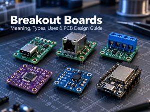
A breakout board is a small printed circuit board that makes an electronic component easier to use, test, and connect. Many modern chips, sensors, connectors, and modules use tiny packages or dense pin spacing that are not friendly for hand wiring, breadboard experiments, or fast prototyping. A breakout board solves this problem by “breaking out” those small or hard-to-access pins into larger pads, pin headers, screw terminals, or standard connectors.

What is a Breakout Board?

A breakout board is a PCB that takes the electrical pins of a component and routes them to easier connection points. The component may be a sensor IC, power chip, communication module, connector, USB interface, ESP32 module, or any other part that needs a more practical interface. In simple terms, a breakout board acts as a bridge between a tiny electronic component and a user-friendly circuit environment.

For example, a small surface-mount IC may have pins spaced only 0.5 mm apart. That is difficult to solder by hand and impossible to place directly into a breadboard. A breakout board mounts that IC on a small PCB and routes each pin to 2.54 mm headers, test pads, or terminal blocks. This makes the component much easier to connect with jumper wires, breadboards, test equipment, or another PCB.

A typical breakout board may include:

  • The main chip, module, sensor, or connector
  • Pin headers or solder pads
  • Power and ground pins
  • Pull-up or pull-down resistors
  • Decoupling capacitors
  • Voltage regulator or level shifting circuit
  • Labels printed on the silkscreen
  • Mounting holes for mechanical installation
What is a Breakout Board?

What is a Breakout Board?

What is a Breakout in Electrical Terms?

In electrical and electronic design, breakout means extending or separating multiple electrical signals from a compact source into more accessible connection points.

The source may be:

  • A fine-pitch IC package
  • A board-to-board connector
  • A cable connector
  • A USB port
  • A camera module connector
  • A microcontroller module
  • A sensor package
  • A test fixture interface

The “breakout” process makes each signal easier to identify, probe, solder, or connect. This is why breakout boards are common in laboratories, repair shops, embedded system development, and PCB prototyping.

In PCB development, breakout can also describe the routing area where traces leave a dense component footprint. For example, when routing a BGA package assembly, engineers may talk about “BGA breakout routing,” which means fan-out routing from the BGA pads to other PCB layers.

Is a Breakout Board a PCB?

Yes, in most cases, a breakout board is a type of PCB. More specifically, it is a small functional PCB designed to expose signals from one component, connector, or module.

A breakout board PCB is usually simpler than a full product PCB. It may not contain a complete system. Instead, it focuses on making one part easier to connect and test.

A breakout board can be used alone, connected to a breadboard, plugged into a development board, or integrated into a larger test fixture. In professional engineering workflows, breakout boards are often used before the final PCB design is completed.

What is the Purpose of a Breakout Board?

The main purpose of a breakout board is to make an electronic component easier to connect, evaluate, and integrate. It reduces the gap between the small physical structure of modern electronics and the practical needs of engineers during development.

1. Easier prototyping

Many ICs and modules are not breadboard-friendly. A breakout board converts small pins into larger headers or pads, allowing fast connection with jumper wires, test clips, or soldered leads.

2. Faster component testing

Before using a new sensor, power IC, connector, or communication chip in a product, engineers often need to check whether it performs as expected. A breakout board provides a convenient test platform.

3. Better access to signals

Breakout boards make signals easier to probe with an oscilloscope, multimeter, logic analyzer, or functional test fixture. This is especially useful during debugging.

4. Reduced soldering difficulty

Fine-pitch SMD parts can be hard to solder manually. A breakout board allows the difficult component to be mounted once, while the user connects to larger and more forgiving pads.

5. Easier system integration

A breakout board can help connect a small module to another system, such as an Arduino, Raspberry Pi, ESP32, industrial controller, or custom test board.

6. Safer development

Some breakout boards include basic protection, such as reverse polarity protection, ESD protection, current-limiting resistors, or level shifting.

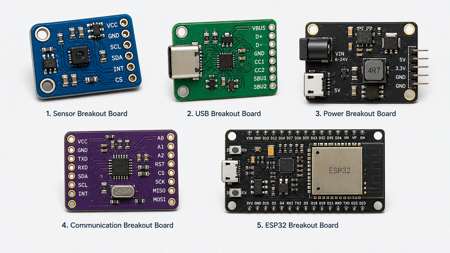
Types of Breakout Boards

Breakout boards come in many forms because electronic components have different electrical and mechanical needs. Below are common types used in prototyping and PCB design.

Types of Breakout Boards

1. Sensor Breakout Board

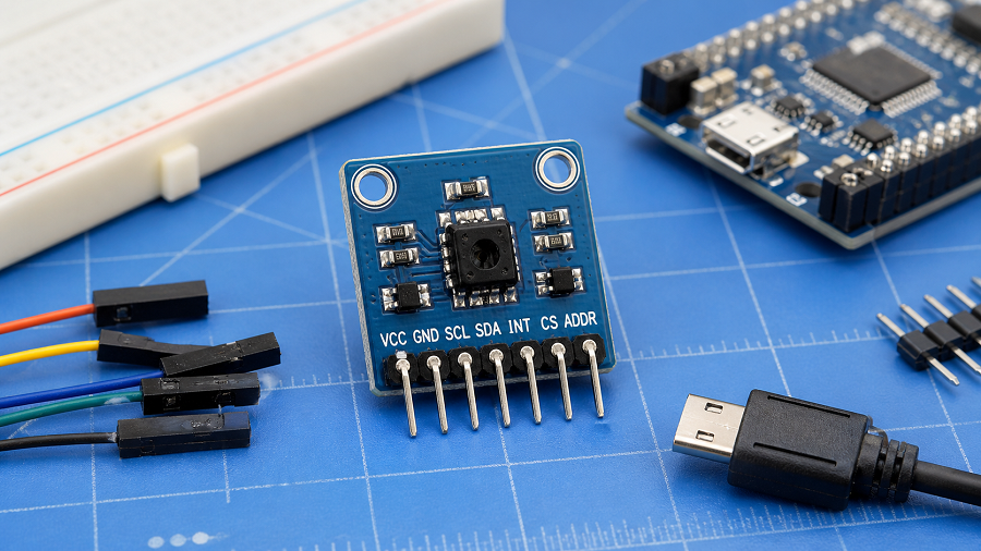
Sensor breakout boards are very popular in embedded systems. They may include temperature sensors, pressure sensors, motion sensors, light sensors, gas sensors, current sensors, or magnetic sensors.

Many sensor ICs use small packages and require supporting parts such as pull-up resistors or capacitors. A breakout board places those parts on the PCB and provides pins for power, ground, and signal communication.

Common interfaces include I2C, SPI, UART, analog output, and digital output.

2. Microcontroller Breakout Board

A microcontroller breakout board exposes the pins of a microcontroller or module. It may support ESP32, STM32, RP2040, ATmega, or other MCU families.

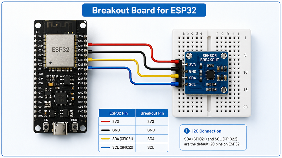
A breakout board for ESP32 is especially useful because ESP32 modules include Wi-Fi, Bluetooth, GPIO, ADC, UART, SPI, I2C, PWM, and power pins. A breakout board helps organize those pins into a more usable layout.

3. Connector Breakout Board

Connector breakout boards expose small or dense connectors to larger pads or headers. Common examples include USB, HDMI, FFC/FPC, RJ45, SD card, SIM card, and board-to-board connectors.

4. Power Breakout Board

Power breakout boards help distribute or adapt power. They may include voltage regulators, screw terminals, fuses, current sense resistors, reverse polarity protection, or DC jack connectors.

They are often used in robotics, LED control, battery systems, and industrial prototypes.

5. Communication Breakout Board

These boards provide access to communication chips or modules, such as RS485, CAN, Ethernet, LoRa, Wi-Fi, Bluetooth, NFC, or USB-to-UART converters.

6. IC Adapter Breakout Board

An IC adapter breakout board converts one package style into another more usable form. For example, it may convert SOP, QFN, TSSOP, MSOP, or DFN packages to DIP-style headers.

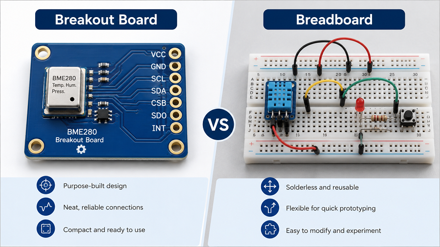
Breakout Board vs Breadboard

The topic of breakout board vs breadboard is common because both are used in prototyping. However, they are not the same.

A breadboard is a solderless platform used to build temporary circuits. A breakout board is a PCB that makes a specific component easier to connect.

A breakout board and a breadboard are often used together. For example, a small sensor breakout board can plug into a breadboard, allowing the user to build a temporary circuit around it.

Breakout Board vs Breadboard

However, for high-speed signals, RF circuits, precision analog circuits, USB, CAN, or power electronics, a breadboard may create poor results due to parasitic capacitance, loose contacts, and uncontrolled wiring. In those cases, a breakout board or custom PCB is a better choice. Here is a detailed comparison between them:

Comparison PointBreakout BoardBreadboard
StructureCustom PCB with routed tracesSolderless plastic board with internal metal clips
Main purposeExpose component pinsBuild temporary circuits
SolderingUsually required for headers or componentsNo soldering needed
Signal qualityBetter than loose breadboard wiringLimited for high-speed or sensitive signals
DurabilityMore stable and repeatableGood for quick experiments, less stable for long-term use
Suitable for SMD partsYesNot directly
Suitable for final productsSometimes used in fixtures or modulesNot suitable for finished products

Typical Breakout Board Features

Although breakout boards vary widely, many of them share similar features.

Pin headers or castellated holes

These allow the board to plug into a breadboard, connect with jumper wires, or solder onto another PCB. Castellated holes are useful when the breakout board needs to be treated like a surface-mount module.

Clear silkscreen labels

Good labeling makes a breakout board easier to use. Pin names such as VCC, GND, SDA, SCL, TX, RX, EN, IO0, 3V3, and VIN should be readable and correctly placed.

Decoupling capacitors

Decoupling capacitors help stabilize power near the IC or module. This is especially important for microcontrollers, sensors, RF modules, and fast-switching components.

Pull-up and pull-down resistors

Some interfaces, such as I2C, reset pins, boot pins, and enable pins, may require defined logic states. Breakout boards often include these resistors.

Voltage regulation

A breakout board may include an LDO regulator or DC-DC converter to accept a wider input voltage and provide the correct operating voltage.

Level shifting

When one system uses 5 V logic and another uses 3.3 V logic, a level shifter may be required. This is common in breakout boards used with Arduino, ESP32, and Raspberry Pi systems.

Protection circuit

ESD diodes, resettable fuses, series resistors, and reverse polarity protection can improve reliability during testing and field use.

How to Connect a Breakout Board?

Connecting a breakout board depends on the component, interface, voltage level, and host controller. Still, most breakout boards follow a similar process.

1. Read the pin labels and datasheet

Before wiring, check the pin names, voltage range, interface type, and current requirements. Do not assume that all breakout boards use the same pin order.

2. Connect power and ground first

Most boards require VCC or VIN and GND. Confirm whether the board accepts 5 V, 3.3 V, or another voltage. ESP32-based systems usually operate at 3.3 V logic, even when some development boards accept 5 V through a regulator.

3. Connect the signal pins

For I2C, connect SDA and SCL.

For SPI, connect MOSI, MISO, SCK, and CS.

For UART, connect TX to RX and RX to TX.

For analog output, connect the signal pin to an ADC input.

For digital output, connect the pin to a GPIO.

4. Check logic voltage compatibility

A 5 V signal connected directly to a 3.3 V ESP32 GPIO may damage the chip. Use level shifting when needed.

breakout board for ESP32

5. Add pull-up resistors when required

Some breakout boards already include pull-up resistors. Others do not. I2C lines usually need pull-ups to the correct logic voltage.

6. Keep wiring short for sensitive signals

Long jumper wires may create noise, ringing, or communication errors. For high-speed signals, a custom PCB is better than loose wiring.

7. Test with simple code or basic measurements

Confirm power voltage, device address, communication response, and basic output before building a larger system.

For a breakout board for ESP32, always pay attention to 3.3 V logic, bootstrapping pins, current demand, antenna clearance, and GPIO functions. Some ESP32 pins have special behavior during startup, so pin selection matters.

Applications and Uses of Breakout Boards

Breakout boards are used across many fields, from hobby electronics to professional engineering.

  • Embedded system development
  • ESP32 and IoT projects
  • PCB prototyping
  • Production testing
  • Repair and reverse engineering
  • Education and training
  • Industrial control prototypes
  • Medical, automotive, and aerospace electronics evaluation

In high-reliability industries, breakout boards may be used for early validation, test planning, component qualification, and interface checking before formal product development.

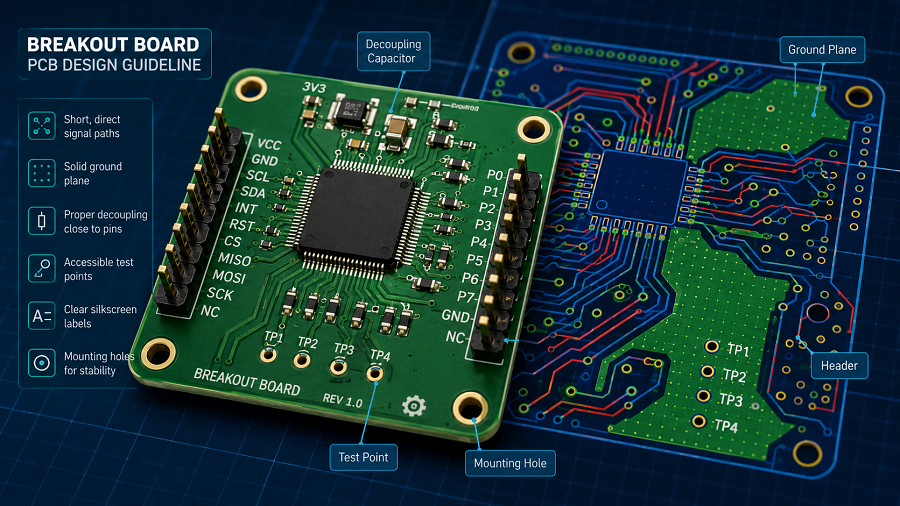
Breakout Board PCB Design Guideline

A good breakout board PCB design should not only expose pins. It should also protect signal quality, simplify assembly, and make debugging easier. Below are practical design guidelines.

Breakout Board PCB Design Guideline

1. Define the purpose before layout

Start by deciding what the board needs to do. Is it only an adapter? Does it need power regulation? Will it support breadboard use? Will it be mounted inside a test fixture? Will it be used by engineers, customers, or production operators?

The purpose affects size, connector choice, silkscreen labeling, mounting holes, and protection circuits.

2. Choose the right connector style

For breadboard use, 2.54 mm through-hole headers are common. For compact integration, castellated holes may be better. For field wiring, screw terminals or spring terminals are easier to handle. For test fixtures, pogo-pin pads may be preferred.

Connector selection should match how the board will actually be used.

3. Keep pinout logical

A good pinout reduces mistakes. Place power and ground pins clearly. Group communication pins together. For example, I2C pins should be near each other, and SPI pins should be organized in a readable sequence.

For ESP32 breakout boards, group GPIO pins by function when possible, such as ADC pins, UART pins, SPI pins, I2C pins, and power pins.

4. Use clear silkscreen

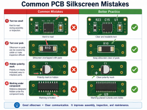
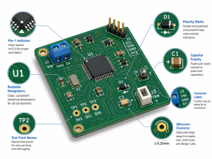
Silkscreen is not decoration. It is part of the user interface. Label every important pin. Mark voltage levels. Indicate pin 1. Add polarity marks for diodes, capacitors, power connectors, and LEDs.

Avoid placing text under components or too close to pads where solder may cover it.

5. Add decoupling capacitors close to power pins

Place decoupling capacitors near the power pins of the IC or module. Short traces help reduce power noise and improve circuit stability.

For many ICs, a 0.1 µF capacitor is placed close to each power pin, with additional bulk capacitance when needed.

6. Consider signal integrity

For low-speed GPIO or simple analog signals, routing is usually straightforward. For USB, high-speed SPI, RF, Ethernet, HDMI, or fast clocks, layout needs more care.

Controlled impedance, short trace length, solid ground reference, differential pair routing, and proper return paths may be required.

7. Use a solid ground plane when possible

Even on a small 2-layer breakout board, a solid ground plane improves stability, reduces noise, and gives signals a better return path.

Avoid cutting the ground plane unnecessarily. Keep high-current paths and sensitive analog signals separated when practical.

8. Protect exposed interfaces

Breakout boards are often handled, touched, rewired, and tested repeatedly. This increases the chance of ESD, reverse connection, or accidental short circuits.

Useful protection methods include:

  • ESD protection diodes for external connectors
  • Series resistors for signal protection
  • Resettable fuse for power input
  • Reverse polarity protection
  • TVS diodes for power or communication lines
  • Clear polarity marking on silkscreen

9. Include test points

Test points are valuable during debugging and manufacturing. At minimum, consider adding test points for power, ground, reset, communication lines, and important control signals.

For production use, test points can support ICT, flying probe testing, or functional test fixtures.

10. Review the design before fabrication

Before sending files to a PCB manufacturer, check:

  • Schematic correctness
  • Footprint accuracy
  • Pin mapping
  • Power polarity
  • DRC errors
  • Silkscreen readability
  • Connector orientation
  • Mounting hole position
  • Board outline
  • Gerber files
  • BOM accuracy
  • Assembly drawing

At EBest Circuit, breakout board PCB projects can be supported from PCB fabrication to assembly and testing. For customers developing sensor modules, ESP32-related hardware, connector adapters, or custom evaluation boards, early DFM review helps catch layout, soldering, and manufacturability issues before production.

FAQs

1. Do you need a breakout board?

You need a breakout board when a component is difficult to connect directly, especially if it uses fine-pitch pins, SMD packaging, dense connectors, or special voltage requirements. A breakout board is also useful when you want to test a component before designing it into a final PCB.

For simple through-hole components, you may not need one. For sensors, modules, USB connectors, ESP32 peripherals, and small IC packages, a breakout board can save time and reduce wiring errors.

2. What is a USB breakout board?

A USB breakout board is a small PCB that exposes the pins of a USB connector to larger pads or headers. It may be used for USB power testing, data line measurement, connector evaluation, repair work, or custom device development.

A USB breakout board may expose VBUS, GND, D+, D-, shield, CC pins, SBU pins, or SuperSpeed differential pairs, depending on whether it uses USB 2.0, USB 3.x, Micro USB, Mini USB, USB-A, or USB Type-C.

3. What is the difference between a breakout board and a development board?

A breakout board usually exposes the pins of one component, connector, sensor, or module. A development board is usually a more complete platform that includes a microcontroller or processor, power circuit, programming interface, reset circuit, clock source, connectors, and sometimes built-in debugging support.

4. How do you choose the right breakout board for ESP32 projects?

To choose the right breakout board for ESP32 projects, check the ESP32 module type, pinout, voltage input, available GPIO pins, USB interface, programming method, mounting style, and antenna clearance.

Also confirm whether the board supports your required functions, such as ADC, I2C, SPI, UART, PWM, battery power, sensor connection, relay control, or display interface. For stable wireless performance, avoid placing copper, metal parts, or tall components too close to the ESP32 antenna area.

5. Can I design a custom breakout board PCB for my own component?

Yes. You can design a custom breakout board PCB for almost any component, including sensors, ICs, connectors, power modules, wireless modules, and display interfaces.

A custom board is useful when standard breakout boards do not match your pinout, size, voltage, connector style, or testing method. For better results, start with the component datasheet, create an accurate schematic, verify the footprint, add proper power filtering, label the pins clearly, and review the Gerber files before fabrication.

You may also like

Best Thermostat Circuit Board Manufacturer, One Stop Assembly Solution

May 6th, 2026

Looking for a reliable thermostat circuit board manufacturer? Choose EBest. We are your premier provider for high quality and reliable thermostat circuit board solutions. With decades of manufacturing expertise and strict quality control systems, we deliver stable, durable and high performance thermostat circuit boards for global customers in various industries.

Thermostat Circuit Board, https://www.bestpcbs.com/blog/2026/05/thermostat-circuit-board/

What are Challenges in Thermostat Circuit Board Design And How to Solve Them?

Here are challenges in thermostat circuit board design and EBest’s solutions:

  • Unstable temperature sensing and inaccurate readings: We use high precision sensor matching circuits and optimized signal acquisition design to ensure stable and accurate temperature detection across different working environments.
  • Signal interference and electromagnetic compatibility issues: We implement strict EMC design, reasonable grounding layout and shielding measures to prevent external interference and ensure stable signal transmission.
  • High power consumption and short service life: We select low power components and optimize circuit architecture to reduce energy use and support longer continuous operation.
  • Poor thermal management and overheating risks: We design enhanced heat dissipation layouts, use high thermal conductivity materials and avoid component heat concentration to ensure stable working temperature.
  • Miniaturization and high integration limitations: We apply HDI design and compact component arrangement to support smaller size and higher integration without losing performance.
  • Environmental adaptability and reliability issues: We strengthen protection circuit design and select industrial grade components to adapt to high temperature, low temperature, humidity and vibration environments.

    Our professional engineering team provides customized thermostat circuit board design services according to your application scenarios, working environment and performance requirements. We conduct full process simulation and verification to ensure stable and long lasting performance. Choose EBest for professional thermostat board design services.

    What Issues Occur in Thermostat Circuit Board Prototype And How to Fix Them?

    Here are issues in thermostat circuit board prototype and EBest’s solutions:

    • Long prototype lead times and delayed project schedules: We provide 24 hour expedited prototyping services to support rapid validation and speed up product development cycles.
    • Low prototype yield and high failure rates: We carry out strict DFM inspection and design optimization before production to effectively reduce defects and improve yield.
    • Inconsistent performance between prototypes: We use standardized processing parameters and stable production lines to ensure consistent performance and dimensions of each prototype.
    • Unreliable test results and incomplete verification: We provide full functional testing, temperature cycling testing and reliability verification to ensure prototypes meet design targets.
    • Poor compatibility between prototype and mass production: We use mass production level processes and materials for prototyping to ensure seamless transition from prototype to mass production.
    • Limited customization for special scenarios: We support flexible customization of materials, layer count, thickness and interfaces to meet special demands of medical, aerospace and industrial applications.

      Our efficient prototype process ensures fast delivery, stable performance and high compatibility for thermostat board prototypes. We support small batch trial production and continuous optimization. Partner with EBest for efficient thermostat circuit board prototype solutions.

      What Problems Exist In Thermostat Circuit Board Assembly And How To Resolve Them?

      Here are challenges in thermostat board prototype and EBest’s solutions:

      • Poor soldering quality: We use automatic SMT assembly lines, combined with AOI and X ray inspection to eliminate cold joints, false soldering and insufficient solder.
      • Component mismatch or counterfeit parts: Our global component sourcing system ensures 100% original authentic components with full material traceability.
      • Low assembly efficiency and long lead times: Standardized assembly processes and streamlined production lines greatly improve efficiency and support fast turnaround.
      • Insufficient testing and reliability risks: We implement full functional testing, aging testing and environmental testing to ensure every board meets performance requirements.
      • Thermal management failure after assembly: We strictly follow thermal design specifications during assembly to ensure consistent heat dissipation performance.
      • Signal interference caused by improper wiring: Our technicians follow EMC design rules during assembly to maintain stable signal transmission.

        Trust EBest for reliable thermostat circuit board assembly services with consistent quality and high reliability.

        Why Choose EBest For Your Best Thermostat Circuit Board Manufacturer?

        EBest focuses on creating real value for customers. We help you reduce costs, shorten lead times, improve product reliability and speed up project launches. Here are reasons why choose EBest for your best thermostat circuit board manufacturer:

        • We help you reduce failure rates and after-sales risks by delivering high stability thermostat circuit board with strict quality control.
        • We provide one-stop service to save your time on coordinating design, prototype, assembly and mass production.
        • We offer fast 24-hour expedited service to help you launch products ahead of schedule and seize market opportunities.
        • We provide customized solutions to meet your specific needs for medical, aerospace and industrial applications.
        • We ensure 100% original components to improve product lifespan and reduce your maintenance cost.
        • We support smooth transition from prototype to mass production to avoid redesign and save your development cost.
        • We provide full technical support from design to after-sales to help you solve problems quickly.
        • We meet global industry certifications to help you enter international markets smoothly.
        • We provide stable large-capacity production to ensure on-time delivery and support your market expansion.
        • We build long-term partnership with continuous optimization to help your products stay competitive.

          What Is A Thermostat Board?

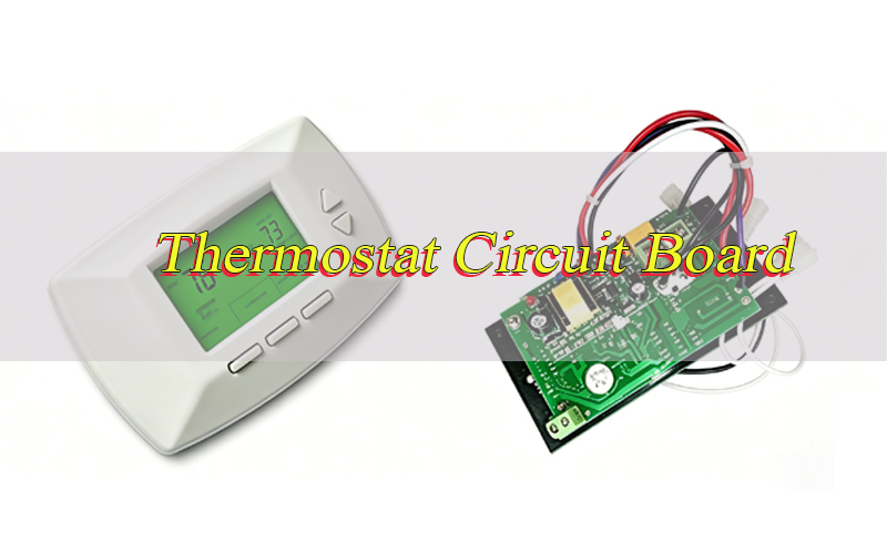
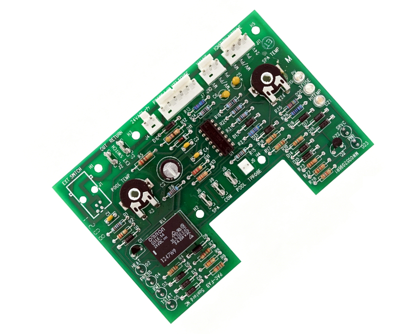
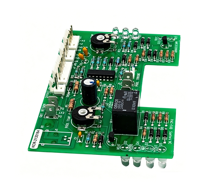
          A thermostat board is the core control circuit that manages temperature sensing, logic processing and load switching in thermostats. It integrates temperature sensors, microcontrollers, power supply circuits, drive circuits and communication modules to achieve accurate and stable temperature control.

          It is widely used in HVAC systems, industrial equipment, medical devices, home appliances and automotive applications. The performance of a thermostat board directly determines the accuracy, stability and reliability of the entire temperature control system.

          Thermostat Circuit Board, https://www.bestpcbs.com/blog/2026/05/thermostat-circuit-board/

          How To Test A Thermostat Circuit Board?

          A complete and standardized test procedure is essential to verify the performance, safety and stability of a thermostat circuit board. Proper testing can identify hidden defects early, ensure accurate temperature control and avoid failures in actual use. The complete test flow includes appearance, electrical, sensing, functional, load, aging and environmental verification.

          Step 1: Visual Inspection – Check for physical damage, burnt components, cold solder joints, lifted pads, trace cracks or foreign contaminants on the thermostat circuit board.

          Step 2: Power Supply Test – Verify input voltage, output voltage, ripple noise and stability. Check for short circuits, open circuits, leakage or abnormal heating in the power module.

          Step 3: Temperature Sensor Test – Test NTC/PTC sensor resistance at different temperatures. Confirm signal linearity, response speed and sampling accuracy of the sensing circuit.

          Step 4: Control Logic Test – Simulate temperature changes to check MCU response, trigger threshold accuracy and action delay. Ensure heating and cooling commands work correctly.

          Step 5: Load Output Test – Connect actual loads such as relays, valves or contactors to verify drive capability, voltage output and switching stability under real working conditions.

          Step 6: Insulation and Safety Test – Perform insulation resistance and withstand voltage tests to ensure electrical safety and compliance with safety standards.

          Step 7: Aging and Stability Test – Run continuous operation for an extended period to confirm long term reliability and consistent performance of the thermostat circuit board.

          Step 8: Environmental Adaptability Test –Test performance under high temperature, low temperature, high humidity and vibration to ensure stable function in harsh environments.

            What Are The Types Of Thermostat Circuit Boards?

            TypeFeaturesApplication
            FR4 Thermostat PCBCost effective and stable performanceGeneral HVAC and home appliances
            HDI Thermostat BoardHigh density and miniaturized designSmart thermostats
            Metal Core Thermostat PCBExcellent heat dissipationHigh power industrial thermostats
            Flexible Thermostat Circuit BoardBendable and space savingPortable temperature control devices

            What Materials Are Used For Thermostat Circuit Boards?

            Selecting the right substrate material is critical to the performance, durability and thermal stability of a thermostat circuit board. Different working environments and application scenarios require specific material properties to ensure long term reliable operation.

            • FR4: Standard substrate with stable performance, good insulation and wide compatibility for general applications.
            • High TG FR4: Suitable for high temperature environments with better thermal resistance and stability.
            • Metal Core Aluminum: Excellent thermal conductivity for high power thermostat applications with large heat generation.
            • Ceramic: High stability, high insulation and high temperature resistance for precision and high reliability scenarios.
            • Flexible Substrates: Bendable and foldable for compact, space constrained and special installation designs.

              What Standards Apply To Thermostat Circuit Boards?

              Thermostat circuit boards must follow strict international and industry specific standards to ensure safety, reliability and market access compliance. These standards cover quality, safety, environmental protection and industry specific requirements.

              • IPC A 600 and IPC 6012: General PCB quality and acceptance standards.

              • UL: Safety certification for electrical and electronic products.
              • RoHS and REACH: Environmental protection and hazardous substance restrictions.
              • IATF 16949: Quality standard for automotive grade thermostat PCB board.
              • ISO 13485: Quality management system for medical thermostat applications.
              • AS9100D: Aerospace industry quality standard for high reliability products.
              • IPC J STD 001: Soldering and assembly process standards.
              Thermostat Circuit Board, https://www.bestpcbs.com/blog/2026/05/thermostat-circuit-board/

                What Are Typical Applications Of Thermostat Circuit Boards?

                Thermostat circuit board products are widely used in many fields that require accurate temperature control. They provide stable control capabilities for devices in daily life, industrial production, medical care and aerospace.

                • Medical devices: Temperature control for diagnostic equipment, patient monitoring systems and medical incubators.
                • Aerospace: Environmental control and temperature regulation in avionics, aircraft systems and satellite equipment.
                • Industrial equipment: Automatic temperature control for production lines, automation equipment and instruments.
                • HVAC systems: Residential and commercial heating, ventilation and air conditioning control systems.
                • Home appliances: Ovens, water heaters, refrigerators and other temperature controlled appliances.
                • Automotive electronics: Temperature management for vehicle air conditioners and battery thermal management systems.
                Thermostat Circuit Board, https://www.bestpcbs.com/blog/2026/05/thermostat-circuit-board/

                  FAQ About Thermostat Circuit Boards

                  Q1: Are thermostats and furnace circuit boards all 24V DC?

                  A1: Most residential thermostats use 24V AC, not 24V DC. Some control boards use 24V DC or 120V/240V AC. Always check the label or schematic before powering your board.

                  Q2: How long do thermostat circuit boards last?

                  A2: A high-quality thermostat circuit board typically lasts 8–15 years. Service life is mainly affected by operating environment, usage frequency, component quality and maintenance.

                  Q3: Why is my thermostat circuit board not working?

                  A3: The most common causes are power failure, sensor damage, component burnout, loose wiring or moisture intrusion. Professional testing can quickly locate and fix the root cause.

                  Q4: Can I repair a thermostat circuit board?

                  A4: Minor issues like loose connections or small component damage can be repaired.Severe damage, burnt circuits or core chip failure require full board replacement.

                  Q5: How to read a thermostat circuit board diagram?

                  A5: A standard diagram clearly marks power input, sensor circuits, control modules and output interfaces. You can identify functions and signal paths step by step for maintenance and troubleshooting.

                  Q6: How to choose the right thermostat circuit board manufacturer?

                  A6: Prioritize experience, complete certifications, one-stop service, strict quality control and customization capability. These core strengths ensure stable quality and reliable support for your project.

                  Request Your Free Quote For Thermostat Circuit Board Today

                  If you need reliable, certified and cost-effective thermostat circuit board solutions, EBest is ready to support your project. Send us your design files, quantity and lead time to get a free, no-obligation quote within 24 hours. Our engineering team will also provide professional DFM suggestions to optimize your design and lower production risks.

                  Contact us now at sales@bestpcbs.com to start your custom thermostat circuit board project.

                  You may also like

                  What is the Process of Underfill Dispensing?

                  May 5th, 2026

                  What is underfill dispensing, and why is it vital for electronic component reliability, especially in consumer, automotive, and aerospace industries? Many manufacturers struggle with costly defects, inconsistent results, and wasted resources when implementing this process. The good news? This blog reveals the secrets to mastering underfill dispensing from core basics to pro-level optimization to eliminate pain points and boost quality. Read on to unlock the key to reliable, efficient underfill application.

                  Underfill Dispensing, https://www.bestpcbs.com/blog/2026/05/underfill-dispensing/

                  What is Underfill Dispensing and Why Is It Critical for Electronic Components?

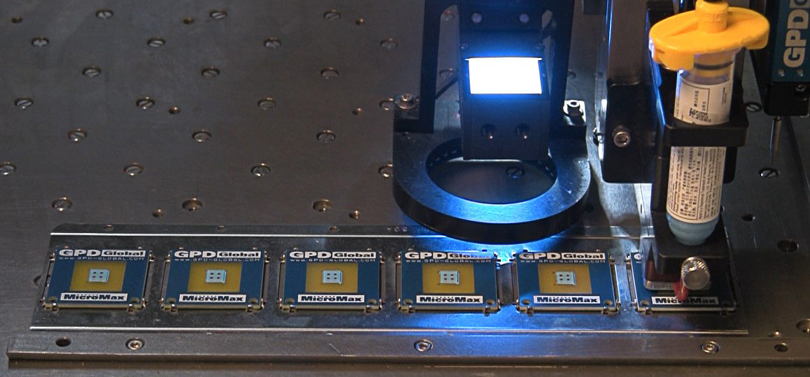
                  Underfill dispensing is a specialized application process that deposits a protective adhesive material beneath electronic components such as BGA, CSP, and flip chip packages. This material flows into the gaps between the component and the printed circuit board, forming a strong bond that reinforces the connection between the component and the board.

                  The primary purpose of underfill dispensing is to protect solder joints from external stressors that can cause failure over time. Electronic components are often exposed to thermal cycling, mechanical vibration, and environmental factors like humidity, which can lead to solder joint fatigue, cracking, or separation. Underfill material acts as a buffer, absorbing thermal expansion differences between the component and the board, reducing stress on solder joints and extending the overall lifespan of the electronic device.

                  Without proper underfill application, electronic components are at high risk of premature failure. This is especially critical in high-reliability industries such as automotive, aerospace, and medical devices, where component failure can lead to safety hazards, costly recalls, or operational downtime. Even in consumer electronics, underfill dispensing ensures devices remain durable through daily use, reducing warranty claims and improving customer satisfaction.

                  What Types of Underfill Dispensing Equipment Are Used in Different Production Scenarios?

                  The right underfill dispensing equipment depends on production volume, component size, precision requirements, and budget constraints. Below are the most common types used in various manufacturing scenarios:

                  • Manual Dispensing Syringes: Ideal for low-volume production, prototyping, or small-batch runs. These are simple, cost-effective tools that require manual operation to control the flow of underfill material. They work best for large components with relaxed precision requirements, as they rely on operator consistency.
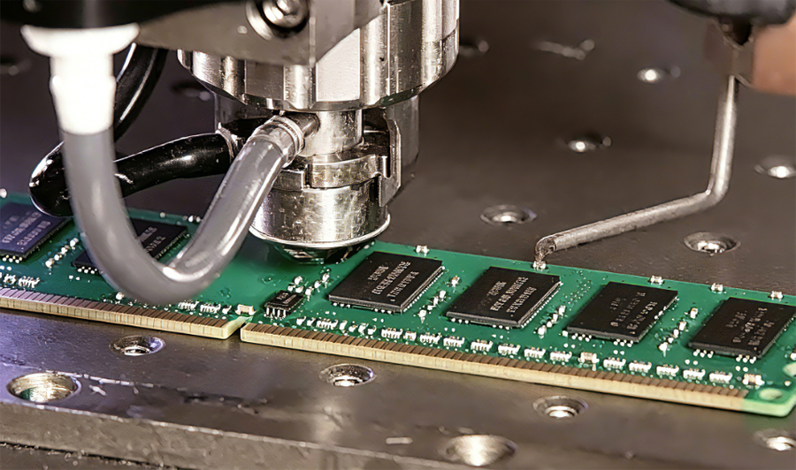
                  • Semi-Automatic Dispensing Systems: Combine manual component loading with automated dispensing. These systems feature a programmable dispenser that controls flow rate, dispense time, and path, reducing operator error. They are suitable for medium-volume production where precision is important but full automation is not yet feasible.
                  • Automatic Vision-Controlled Dispensing Machines: Equipped with cameras and advanced software to align components and dispense underfill with high precision. These machines integrate with production lines, enabling high-volume, high-accuracy dispensing for small components like micro BGAs and flip chips. They are widely used in consumer electronics manufacturing.
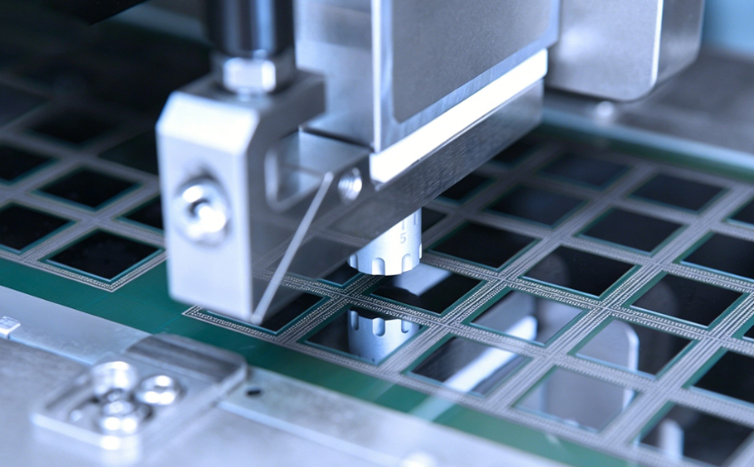
                  • Jet Dispensing Systems: Use a non-contact method to deposit underfill material, eliminating the risk of component damage from needle contact. They offer fast dispensing speeds and high precision, making them ideal for high-volume production of miniaturized components, such as those used in smartphones and wearables.
                  • Vacuum-Assisted Dispensing Equipment: Designed for components with tight gaps or complex geometries where air entrapment is a concern. These systems use vacuum pressure to draw underfill material into hard-to-reach areas, ensuring complete coverage and reducing defects like voids.

                  How to Choose the Right Underfill Dispensing Pattern for BGA and Flip Chip Applications?

                  Selecting the correct underfill dispensing pattern is critical to ensuring complete coverage, minimizing defects, and optimizing production efficiency. The choice depends on component type, size, gap height, and underfill material properties. Below are guidelines for BGA and flip chip applications:

                  • Single-Side Line Dispensing: Apply a continuous line of underfill along one edge of the BGA or flip chip. This pattern works best for components with large gap heights (greater than 50μm) and high-flow underfill materials. It is simple to program and ideal for medium-sized BGAs.
                  • Two-Side Line Dispensing: Dispense underfill along two opposite edges of the component. This pattern reduces filling time by allowing underfill to flow from two directions, ensuring faster coverage. It is recommended for larger BGAs (greater than 15mm) or components with moderate gap heights.
                  • Corner Dot Dispensing: Deposit small dots of underfill at each corner of the component. This pattern is suitable for small BGAs and flip chips with tight gap heights (less than 30μm). The dots flow inward to cover the entire component bottom, reducing the risk of overflow.
                  • Perimeter Dispensing: Apply a continuous line of underfill around the entire perimeter of the component. This pattern ensures uniform coverage and is ideal for components with irregular shapes or those requiring maximum protection against environmental factors. It works well with low-flow underfill materials.
                  • Spiral Dispensing: Create a spiral pattern of underfill on the component surface, which spreads evenly as it flows into the gaps. This pattern is effective for components with high-density solder joints, as it ensures no areas are missed and reduces the risk of voids.
                  • Center Dispensing: Deposit underfill at the center of the component, allowing it to flow outward to the edges. This pattern is suitable for flip chips with small footprints and uniform gap heights. It minimizes underfill waste and ensures consistent coverage.
                  • Staggered Line Dispensing: Apply alternating lines of underfill along the component edges, which helps distribute the material more evenly and reduces filling time. This pattern is recommended for large BGAs with varying gap heights or uneven solder joint distributions.
                  • Custom Pattern Dispensing: Program a unique pattern tailored to the specific component geometry. This is necessary for complex components with asymmetrical designs, cutouts, or non-standard shapes, ensuring complete coverage in all critical areas.

                  What Preparations Are Needed Before Starting the Underfill Dispensing Process?

                  Proper preparation is essential to avoid defects and ensure consistent underfill dispensing results. The following steps must be completed before starting the process:

                  • Inspect Components and PCBs: Check for any damage, contamination, or misalignment. Components with bent pins, cracked solder joints, or debris on the bottom will cause underfill defects. PCBs should be free of dust, flux residues, and moisture.
                  • Store Underfill Material Correctly: Underfill adhesives are often temperature-sensitive and require refrigerated storage (2–8℃) to maintain their properties. Allow the material to reach room temperature (25±2℃) before use to prevent moisture condensation and ensure proper flow.
                  • Calibrate Dispensing Equipment: Verify that the dispenser’s flow rate, dispense time, and needle position are calibrated to the required specifications. Use a scale to measure dispensed material volume and adjust settings as needed to ensure accuracy.
                  • Prepare the Work Environment: Maintain a clean, temperature-controlled workspace (25±2℃, 40–60% RH) to prevent moisture absorption and ensure consistent underfill flow. Use HEPA filters to reduce dust and contaminants.
                  • Test Underfill Material Compatibility: Ensure the underfill material is compatible with the component and PCB materials. Conduct a small test run to check for adhesion issues, flow rate, and curing time.
                  • Set Up Fixtures and Alignment Tools: Use fixtures to secure PCBs and components in place, ensuring proper alignment during dispensing. Misalignment can lead to uneven underfill coverage and solder joint stress.
                  • Check Curing Equipment: Verify that ovens or curing stations are set to the correct temperature and time settings, as specified by the underfill material manufacturer. Improper curing will compromise the adhesive’s strength and protective properties.
                  Underfill Dispensing, https://www.bestpcbs.com/blog/2026/05/underfill-dispensing/

                  How Does Pre-Heating Affect the Underfill Dispensing Process and Final Results?

                  Pre-heating is a critical step in underfill dispensing, as it directly impacts material flow, void formation, and curing quality. The following points outline its key effects:

                  • Reduces Underfill Viscosity: Pre-heating the PCB and component lowers the viscosity of the underfill material, allowing it to flow more easily into the gaps between the component and the board. This ensures complete coverage, especially for components with tight gap heights (less than 50μm).
                  • Minimizes Void Formation: Moisture trapped in the PCB or component can evaporate during pre-heating, reducing the risk of voids in the underfill layer. Voids weaken the bond between the component and the board, increasing the chance of solder joint failure.
                  • Improves Adhesion: Pre-heating cleans the surface of the PCB and component by removing flux residues and contaminants, enhancing the adhesion of the underfill material. This results in a stronger bond and better long-term reliability.
                  • Controls Curing Time: Consistent pre-heating ensures the underfill material cures uniformly, preventing uneven curing that can lead to stress cracks. It also shortens the overall curing time, improving production efficiency.
                  • Prevents Thermal Shock: Gradual pre-heating reduces thermal shock to the component and PCB, which can cause damage to solder joints or the component itself. This is especially important for delicate components like flip chips.
                  • Optimizes Flow Rate: Pre-heating at the correct temperature (typically 80–120℃, depending on the underfill material) ensures a consistent flow rate, reducing the risk of overflow or incomplete filling. Incorrect pre-heating temperatures can either slow flow (too low) or cause premature curing (too high).

                  What is the Process of Underfill Dispensing?

                  Underfill dispensing follows a structured, step-by-step process to ensure consistency and quality. Each step must be executed precisely to avoid defects and ensure optimal performance:

                  Step 1: Component and PCB Preparation. Clean and inspect the PCB and component to remove any contaminants, dust, or flux residues. Secure the PCB in a fixture to ensure stability during dispensing.

                  Step 2: Pre-Heating. Place the PCB and component in a pre-heating station set to the manufacturer’s recommended temperature (80–120℃). Hold the temperature for 5–10 minutes to remove moisture and reduce underfill viscosity.

                  Step 3: Equipment Setup. Load the underfill material into the dispensing equipment and calibrate the flow rate, dispense time, and needle position. Ensure the needle is aligned with the component edge to prevent damage.

                  Step 4: Dispensing. Execute the selected dispensing pattern (e.g., line, dot, perimeter) to deposit the underfill material. Monitor the flow to ensure uniform coverage and avoid overflow or underfilling.

                  Step 5: Flow and Wetting. Allow the underfill material to flow into the gaps between the component and the PCB. This process, known as capillary flow, typically takes 1–5 minutes depending on the material and gap height.

                  Step 6: Inspection. Use visual inspection or X-ray imaging to check for voids, incomplete coverage, or overflow. Reject or rework any components that do not meet quality standards.

                  Step 7: Curing. Place the PCB and component in a curing oven set to the recommended temperature (120–150℃) for the specified time (30–60 minutes). This hardens the underfill material, forming a strong bond.

                  Step 8: Post-Curing Inspection. Conduct a final inspection to verify the underfill layer’s integrity, adhesion, and absence of defects. Ensure the component is securely bonded to the PCB and meets all performance requirements.

                   Underfill Dispensing, https://www.bestpcbs.com/blog/2026/05/underfill-dispensing/

                  What are the Parameters to Control During Underfill Dispensing?

                  Controlling parameters during underfill dispensing is critical to achieving consistent results and minimizing defects. The following table outlines the essential parameters, their recommended ranges, and their impact:

                  ParameterRecommended RangeImpact
                  Flow Rate0.1–1.0 mL/minControls the amount of underfill dispensed per minute. Too high causes overflow; too low leads to incomplete coverage.
                  Dispense Time0.5–5.0 secondsDetermines the volume of underfill deposited. Incorrect times result in underfilling or overflow.
                  Needle Height0.5–2.0 mm above componentAffects material placement. Too low damages components; too high causes uneven dispensing.
                  Pre-Heating Temperature80–120℃Reduces viscosity and moisture. Too low slows flow; too high causes premature curing.
                  Curing Temperature120–150℃Ensures proper hardening. Too low results in weak adhesion; too high damages components.
                  Curing Time30–60 minutesDetermines underfill strength. Insufficient time leads to incomplete curing; excess time wastes production resources.
                  Underfill Viscosity500–2000 cP at 25℃Affects flowability. Too high prevents gap filling; too low causes overflow.
                  Ambient Temperature23–27℃Maintains consistent material properties. Fluctuations cause viscosity changes and inconsistent dispensing.

                  What Industry Standards Should Be Followed in the Underfill Dispensing Process?

                  Adhering to industry standards ensures underfill dispensing meets quality, reliability, and safety requirements. The following standards are widely recognized and followed in manufacturing:

                  • IPC-7095: Provides guidelines for the design and implementation of underfill processes for flip chip and BGA components. It covers material selection, process parameters, and quality requirements.
                  • IPC-A-610: Outlines acceptability criteria for electronic assemblies, including underfill application. It specifies allowable defects, such as voids, overflow, and incomplete coverage.
                  • ISO 9001: Ensures a quality management system is in place for underfill dispensing, covering process control, documentation, and continuous improvement.
                  • JEDEC J-STD-020: Details requirements for the handling and processing of moisture-sensitive components, including pre-heating and storage guidelines for underfill materials.
                  • IPC-6012: Specifies performance requirements for rigid printed circuit boards, including surface cleanliness standards that impact underfill adhesion.
                  • Automotive Electronics Council (AEC-Q100): Applies to automotive electronic components, requiring underfill dispensing to meet strict reliability standards for thermal cycling and mechanical stress.

                  How to Avoid Common Defects in the Underfill Dispensing Process?

                  Common defects in underfill dispensing can be avoided through proper process control, equipment maintenance, and material management. The following steps address the most frequent issues:

                  • Voids: Ensure proper pre-heating to remove moisture, use vacuum-assisted dispensing for tight gaps, and select underfill materials with low volatility. Avoid excessive dispense speed, which can trap air.
                  • Incomplete Coverage: Calibrate flow rate and dispense time to ensure sufficient material volume, select the correct dispensing pattern for the component, and verify underfill viscosity is within the recommended range.
                  • Overflow: Adjust needle height and dispense time to reduce material volume, use a perimeter or dot pattern to control flow, and ensure the component is properly aligned to prevent material spread.
                  • Poor Adhesion: Clean components and PCBs thoroughly to remove contaminants, use compatible underfill materials, and ensure proper pre-heating and curing temperatures.
                  • Curing Defects: Follow the manufacturer’s curing guidelines for temperature and time, ensure the curing oven has uniform heat distribution, and avoid interrupting the curing process.
                  • Solder Joint Damage: Use non-contact jet dispensing for delicate components, adjust needle height to prevent contact, and avoid excessive pre-heating temperatures.

                  What is the Difference Between Capillary and Non-Flow Underfill Dispensing Processes?

                  Capillary and non-flow underfill dispensing are the two primary methods used in electronic manufacturing, each with distinct advantages and applications. The following table highlights their differences, and additional details explain their use cases:

                  CharacteristicCapillary Underfill DispensingNon-Flow Underfill Dispensing
                  Flow MechanismRelies on capillary action to draw underfill into gaps between component and PCBUses pressure to force underfill into gaps, no capillary action required
                  Material TypeLow-viscosity, unfilled or lightly filled adhesivesHigh-viscosity, filled adhesives (contains spherical silicon powder)
                  Component CompatibilityIdeal for BGAs, flip chips with small gap heights (20–50μm)Suitable for large components, high-gap heights (50–100μm), and high-density assemblies
                  Production SpeedSlower, due to reliance on capillary flowFaster, as pressure-driven flow reduces filling time
                  Void RiskHigher, if air is trapped during flowLower, as pressure helps eliminate air pockets
                  CostLower material and equipment costsHigher material costs, requires specialized pressure-driven equipment

                  How to Calibrate Underfill Dispensing Equipment for Optimal Precision?

                  Proper calibration of underfill dispensing equipment ensures consistent material deposition, reduces defects, and extends equipment lifespan. The following steps outline the calibration process in detail:

                  • Clean the Dispensing System: Remove any residual underfill material from the needle, syringe, and lines. Use a compatible solvent to dissolve dried material and ensure no clogs or blockages.
                  • Verify Needle Alignment: Use a vision system or alignment tool to check that the needle is perpendicular to the PCB surface and aligned with the component edge. Adjust the needle position to ensure precise material placement.
                  • Calibrate Flow Rate: Dispense a known volume of underfill material onto a scale and measure the time taken. Calculate the flow rate and adjust the equipment settings to match the recommended range (0.1–1.0 mL/min).
                  • Test Dispense Volume: Dispense multiple samples (5–10) and measure each volume with a scale. Ensure the volume is consistent (±5% variation) and adjust dispense time if needed.
                  • Check Pressure Settings: Verify that the air pressure used to drive the underfill material is stable and within the manufacturer’s recommended range. Fluctuations in pressure cause inconsistent flow.
                  • Calibrate Temperature Controls: Ensure the pre-heating station and curing oven maintain the correct temperature. Use a calibrated thermometer to verify accuracy and adjust settings if deviations are found.
                  • Test with Mock Components: Use a mock PCB and component to simulate the dispensing process. Inspect the underfill coverage and adjust parameters to ensure uniform deposition.
                  • Document Calibration Results: Record all calibration settings, including flow rate, dispense time, pressure, and temperature. Keep a log to track calibration frequency and any adjustments made.
                  • Schedule Regular Calibration: Calibrate the equipment at least once per week, or more frequently if production volume is high or defects increase. This ensures consistent performance over time.

                  How to Optimize the Underfill Dispensing Process for Higher Efficiency and Reliability?

                  Optimizing underfill dispensing reduces production time, lowers costs, and improves product reliability. The following strategies address key areas for improvement:

                  • Automate the Process: Upgrade to automatic vision-controlled or jet dispensing systems to reduce operator error, increase production speed, and improve precision. Automation also allows for 24/7 operation, boosting throughput.
                  • Optimize Dispensing Patterns: Select the most efficient pattern for each component type. For example, use two-side line dispensing for large BGAs to reduce filling time, or corner dot dispensing for small flip chips to minimize material waste.
                  • Use High-Quality Underfill Materials: Choose materials with consistent viscosity, low volatility, and good adhesion properties. High-quality materials reduce defects like voids and poor adhesion, lowering rework costs.
                  • Implement Real-Time Monitoring: Use sensors and cameras to monitor the dispensing process in real time. Detect defects like overflow or incomplete coverage early, allowing for immediate adjustments.
                  • Optimize Pre-Heating and Curing: Adjust pre-heating and curing parameters to reduce cycle time without compromising quality. Use convection ovens for uniform heat distribution and faster curing.
                  • Train Personnel: Ensure all operators are familiar with equipment operation, calibration, and defect detection. Proper training reduces human error and ensures consistent process execution.
                  • Implement Preventive Maintenance: Regularly clean and maintain dispensing equipment, including needles, syringes, and lines. Replace worn parts (e.g., needles, O-rings) to prevent malfunctions and defects.
                  • Analyze Defect Data: Track and analyze defect trends to identify root causes. Use this data to adjust process parameters, material selection, or equipment settings, reducing future defects.
                  • Integrate with Production Systems: Connect underfill dispensing equipment to other production systems (e.g., pick-and-place, inspection) for seamless workflow. This reduces bottlenecks and improves overall production efficiency.
                  Underfill Dispensing, https://www.bestpcbs.com/blog/2026/05/underfill-dispensing/

                  FAQs About Underfill Dispensing Process

                  Q1: How often should underfill dispensing equipment be calibrated?

                  A1: Underfill dispensing equipment should be calibrated at least once per week for high-volume production, or every two weeks for low-volume runs. Calibrate more frequently if defects increase, equipment is moved, or underfill material is changed.

                  Q2: Can underfill dispensing be used for all electronic components?

                  A2: No, underfill dispensing is primarily used for components with solder joints that are vulnerable to stress, such as BGAs, CSPs, and flip chips. It is not necessary for through-hole components or surface-mount components with large solder joints.

                  Q3: What causes voids in underfill dispensing and how to fix them?

                  A3: Voids are caused by trapped air, moisture, or excessive dispense speed. Fix them by increasing pre-heating time to remove moisture, using vacuum-assisted dispensing, reducing dispense speed, and selecting underfill materials with low volatility.

                  Q4: How long does underfill dispensing take to complete?

                  A4: The total time depends on component size, gap height, and dispensing method. A typical cycle (pre-heating, dispensing, flow, curing) takes 45–90 minutes, with dispensing itself taking 1–5 minutes per component.

                  Q5: What is the best underfill material for automotive electronic components?

                  A5: Automotive components require underfill materials with high thermal stability, low coefficient of thermal expansion (CTE), and resistance to harsh environments. Epoxy-based underfills with ceramic fillers are recommended, as they provide excellent adhesion and stress resistance.

                  Q6: How to handle underfill material that has expired?

                  A6: Expired underfill material should not be used, as it may have reduced viscosity, poor adhesion, or inconsistent curing. Dispose of expired material according to local regulations and use fresh material stored at the recommended temperature.

                  Q7: Can underfill dispensing be done manually for high-volume production?

                  A7: Manual dispensing is not recommended for high-volume production. It is slow, prone to operator error, and results in inconsistent coverage. Automatic or semi-automatic systems are better suited for high-volume runs.

                  Q8: How to check if underfill has cured properly?

                  A8: Properly cured underfill is hard to the touch, has no tackiness, and adheres firmly to the component and PCB. Use a hardness tester to verify curing, or conduct a peel test to check adhesion strength. Visual inspection can also identify incomplete curing (tacky or discolored material).

                  You may also like

                  What is a Lead Frame Package? Lead Frame Package vs Substrate Package

                  May 5th, 2026

                  Choosing the wrong semiconductor packaging leads to costly delays, wasted resources and compromised reliability, but how do lead frame package compare to substrate solutions? For semiconductor professionals, this guide covers all key details about lead frame packages from structure and manufacturing to types and substrate comparisons to help you avoid errors and make confident, cost-effective decisions.

                  Lead Frame Package, https://www.bestpcbs.com/blog/2026/05/lead-frame-package/

                  What is a Lead Frame Package (LFP) in Semiconductor Manufacturing?

                  A lead frame package is a semiconductor packaging solution that uses a metal frame to connect the internal chip to external circuitry. It serves as the bridge between the semiconductor die and the printed circuit board, facilitating electrical signal transmission, providing physical support for the chip, and protecting the die from environmental damage such as moisture and dust.

                  Unlike more complex packaging solutions, lead frame packages rely on a simple, cost effective design that makes them ideal for a wide range of low to mid complexity semiconductor devices. They are widely used in consumer electronics, automotive components, and industrial equipment, where reliability and cost efficiency are top priorities.

                  The core function of a lead frame package is to route electrical signals from the chip’s bond pads to the external leads, which are then soldered to the PCB. This connection ensures the chip can communicate with other components in the system, while the package itself shields the die from mechanical stress and environmental hazards that could degrade performance or cause failure.

                  What are the Components of a Lead-Frame Package Structure?

                  A lead frame package consists of several key components that work together to ensure reliable performance and protection. Each component has a specific role, and any defect in these parts can lead to package failure or reduced functionality.

                  ComponentDescriptionFunction
                  Lead FrameThin metal sheet (typically copper or copper alloy) with precision-cut leads and a die padSupports the die, routes electrical signals, and dissipates heat from the chip
                  Semiconductor DieThe core semiconductor chip that contains the active circuitryPerforms the primary electrical function of the device (e.g., amplification, switching)
                  Die Attach MaterialAdhesive (epoxy, silver paste, or solder) that bonds the die to the lead frame’s die padSecures the die in place, provides thermal conductivity, and ensures electrical isolation where needed
                  Wire BondsThin metal wires (gold, copper, or aluminum) with diameters ranging from 15-50 μmConnect the die’s bond pads to the lead frame’s inner leads, enabling signal transmission
                  Mold CompoundEpoxy-based thermosetting material that encapsulates the die, wire bonds, and inner leadsProtects internal components from moisture, dust, mechanical stress, and chemical damage
                  External LeadsExtended portions of the lead frame that extend outside the mold compoundConnect the lead frame package to the PCB, enabling electrical connection to the larger system

                  What Materials are Used for Lead Frame Packaging and Why?

                  Selecting the right materials for lead frame packaging is critical to its performance, reliability and cost-effectiveness. Key factors like electrical conductivity, thermal performance, cost and manufacturing compatibility directly impact how well the package serves its intended use. Below, we break down the most common materials for lead frame packaging, including their properties, advantages and ideal use cases.

                  • Copper and Copper Alloys: The most common lead frame materials. Copper has excellent electrical and thermal conductivity, ideal for high-power chips. Alloys like Cu-Ni-Si and Cu-Sn boost mechanical strength and corrosion resistance, widely used in automotive and industrial applications requiring durability.
                  • Gold: Primarily used for wire bonds, offering superior conductivity, corrosion resistance and bond reliability. It is ideal for high-reliability applications like medical devices and aerospace, with easier manufacturability to reduce bond failure risk.
                  • Aluminum: A cost-effective alternative to gold for wire bonds, with good conductivity. It is widely used in consumer electronics and compatible with high-volume manufacturing.
                  • Epoxy Mold Compounds: Thermosetting materials that encapsulate the die and wire bonds, providing protection against moisture and mechanical stress. They offer good thermal stability and electrical insulation, with formulations for diverse applications including high-temperature automotive use.
                  • Die Attach Epoxy: Bonds the die to the lead frame’s die pad, with high thermal conductivity to prevent overheating and strong adhesion. Silver-filled epoxies are used for high-power devices to enhance thermal performance.

                  What is the Full Manufacturing Process of a Lead Frame Package?

                  The manufacturing process of a lead frame package involves several sequential steps, each critical to ensuring the final product meets performance and reliability standards. Following these steps precisely reduces defects and ensures consistent quality across production batches.

                  Step 1: Lead Frame Fabrication: The process starts with a thin metal sheet (typically copper or copper alloy) that is cut into the desired shape using either stamping or etching. Stamping is used for high volume production, as it is fast and cost effective, while etching is used for more complex lead frame designs with finer pitches. The lead frame is then cleaned and plated with a thin layer of nickel or tin to improve corrosion resistance and solderability.

                  Step 2: Die Attach: The semiconductor die is attached to the lead frame’s die pad using die attach epoxy or silver paste. The die is carefully placed on the die pad, and the assembly is heated to cure the adhesive. This step ensures the die is securely bonded and that heat can transfer efficiently from the die to the lead frame.

                  Step 3: Wire Bonding: Thin metal wires (gold, aluminum, or copper) are used to connect the die’s bond pads to the lead frame’s inner leads. This is done using either ultrasonic bonding or thermosonic bonding, which creates a strong, reliable electrical connection. The wire bonds must be precisely placed to avoid short circuits and ensure optimal signal transmission.

                  Step 4: Molding: The die, wire bonds, and inner leads are encapsulated in an epoxy mold compound. The assembly is placed in a mold, and the mold compound is injected under high pressure and temperature. The compound cures to form a protective shell around the internal components, shielding them from environmental damage.

                  Step 5: Post Mold Cure: After molding, the package is heated in an oven to fully cure the mold compound. This step improves the mechanical strength and thermal stability of the package, ensuring it can withstand the stresses of subsequent manufacturing steps and application use. The post mold cure typically takes 8-12 hours at temperatures between 150-175°C.

                  Step 6: Lead Trimming and Forming: The external leads of the lead frame are trimmed to the desired length and bent into the appropriate shape (e.g., J lead, gull wing). This step ensures the leads can be easily soldered to the PCB and fit within the device’s form factor. Precision trimming and forming are critical to avoid lead damage and ensure consistent lead geometry.

                  Step 7: Plating: The external leads are plated with a thin layer of tin, tin lead, or gold to improve solderability and corrosion resistance. Tin plating is the most common, as it is cost effective and compatible with most soldering processes. The plating thickness is carefully controlled to ensure optimal performance.

                  Step 8: Testing and Inspection: The finished lead frame packages are tested for electrical performance, including continuity, insulation resistance, and functionality. They are also inspected for physical defects such as mold cracks, wire bond failures, and lead damage. Packages that fail testing are discarded, while those that pass are prepared for packaging and shipment.

                  Lead Frame Package, https://www.bestpcbs.com/blog/2026/05/lead-frame-package/

                  What are the Most Common Types of Lead Frame Packaging for Electronics?

                  Lead frame packages come in various types, each designed for specific applications and chip requirements. The choice of package type depends on factors such as the number of I/O pins, chip size, power requirements, and form factor constraints.

                  • Dual In Line Package (DIP): One of the oldest and most common lead frame package types. DIP packages have leads on both sides of the mold, arranged in a straight line. They are available in plastic or ceramic versions and are widely used in through hole mounting applications. DIP packages are ideal for low pin count devices (4-40 pins) such as logic gates and voltage regulators.
                  • Small Outline Package (SOP): A surface mount lead frame package with leads on two sides, bent into a gull wing shape. SOP packages are smaller than DIP packages, making them suitable for compact electronic devices such as smartphones and tablets. They are available in various sizes, including SOIC (Small Outline Integrated Circuit) and SSOP (Shrink Small Outline Package), and support pin counts from 8-48.
                  • Quad Flat Package (QFP): A surface mount package with leads on all four sides, bent into a gull wing shape. QFP packages support higher pin counts (44-208 pins) than SOP packages, making them suitable for more complex devices such as microcontrollers and ASICs. They are widely used in automotive and industrial applications where high I/O count is required.
                  • Plastic Leaded Chip Carrier (PLCC): A square surface mount package with J shaped leads on all four sides. PLCC packages have a cavity in the center where the die is mounted, providing excellent protection for the chip. They are used in applications where space is limited and high reliability is required, such as medical devices and aerospace components.
                  • TO Package (Transistor Outline): A lead frame package designed specifically for discrete components such as transistors, diodes, and voltage regulators. TO packages have a metal case (for high power devices) or plastic case (for low power devices) and a small number of leads (2-6). They are widely used in power electronics and industrial applications.
                  • Chip Scale Package (CSP) Lead Frame Variant: A compact lead frame package where the package size is nearly the same as the die size. These packages are used in ultra compact devices such as wearables and smartphones, where space is at a premium. They support high pin counts and offer excellent thermal performance.

                  Is a Stacked Chip Scale Package (SCSP) a Type of Lead Frame Package?

                  No, a Stacked Chip Scale Package (SCSP) is not a type of lead frame package. SCSP is a advanced packaging solution that belongs to the substrate based packaging category, not the lead frame based category.

                  SCSP is designed to stack multiple chips vertically in a single package, reducing the overall footprint and increasing integration density. This is achieved using a substrate (typically a thin, high density interposer) to connect the stacked chips, rather than a metal lead frame. The substrate provides finer pitch interconnections between the chips, enabling higher I/O density and better signal integrity.

                  While some SCSP variants may use lead frame like components for external connections, the core structure of SCSP relies on a substrate, not a lead frame. This distinction is critical for professionals selecting packaging solutions, as substrate based packages like SCSP are better suited for high density, high performance applications, while lead frame packages are ideal for cost sensitive, low to mid complexity devices.

                  Another key difference is that SCSP supports vertical stacking of multiple chips, which is not feasible with traditional lead frame packages. Lead frame packages are typically designed for a single chip, although some variants can accommodate multiple chips in a side by side arrangement. SCSP’s vertical stacking capability makes it ideal for applications such as memory modules and high performance SoCs (System on Chips).

                  What Should Be Considered in Lead Frame Package Design?

                  Designing a lead frame package requires careful consideration of multiple factors to ensure optimal performance, reliability, and manufacturability. Below are the key design considerations:

                  • Pin Count and Pitch: The number of I/O pins and their pitch must match the chip’s requirements and PCB design. Lead frame packages are practical for 4-200 pins; exceeding 200 pins increases complexity and defects. Standard lead pitches range from 0.5 mm to 1.27 mm (0.5 mm minimum), with finer pitches requiring more costly etching. Low pin count devices suit DIP packages, while mid-range pin counts require QFP packages to avoid lead overcrowding and signal interference.
                  • Thermal Management: The package must efficiently dissipate chip heat. Copper lead frames offer superior thermal conductivity, while optimizing die pad size and adding thermal vias enhance heat dissipation. High-power devices benefit from integrated copper heat sinks to prevent overheating.
                  • Mechanical Stress: The package must withstand manufacturing and application stress, especially thermal cycling. Lead frames need sufficient tensile strength (copper alloys like Cu-Ni-Si are suitable), while mold compound and die attach materials should match the chip’s CTE to prevent cracking and delamination.
                  • Electrical Performance: Lead frame design must minimize signal delay, crosstalk, and EMI. Optimizing lead length and spacing reduces interference, while shielded leads and proper grounding are critical for EMI-sensitive applications.
                  • Manufacturability: The design must be compatible with standard processes (stamping, etching, wire bonding) to avoid extra costs. Stamping is ideal for high-volume production, while etching suits complex designs. Using standard wire diameters ensures high bond yield and reduces rework.
                  • Environmental Requirements: The package must withstand the target application’s environment. Automotive packages meet AEC-Q100 standards, industrial packages resist moisture per IPC-6012, and medical packages use biocompatible materials and withstand sterilization.
                  • Cost: Balance performance and cost by choosing appropriate materials and designs. Copper lead frames and aluminum wire bonds reduce costs for consumer electronics, while gold bonds are worthwhile for high-reliability applications. High-volume production lowers unit costs.
                  • PCB Compatibility: External leads must match PCB mounting technology. SMT leads use gull wing or J shapes, while through-hole leads have specific diameters. Precise lead length tolerance ensures consistent soldering.
                  • Reliability Standards: The package must meet industry standards (JEDEC JESD47, IPC-6012, IPC-610) to ensure field performance and reduce failure rates, protecting brand reputation and warranty costs.
                  Lead Frame Package Design, https://www.bestpcbs.com/blog/2026/05/lead-frame-package/

                  What are the Advantages and Limitations of Lead Frame Packaging?

                  Lead frame packages offer several key advantages that make them a popular choice for many semiconductor applications, but they also have limitations that restrict their use in certain high performance or high density scenarios.

                  Advantages of Lead Frame Packaging:

                  • Cost Effective: Lead frame packages are simpler to manufacture than substrate based packages, resulting in lower production costs. This makes them ideal for cost sensitive applications such as consumer electronics.
                  • High Reliability: The simple design and robust materials used in lead frame packages make them highly reliable, even in harsh environments. They are resistant to mechanical stress, moisture, and temperature extremes.
                  • Good Thermal Performance: Copper lead frames offer excellent thermal conductivity, allowing for efficient heat dissipation from the chip. This is critical for high power devices that generate significant heat.
                  • Easy to Manufacture: Lead frame packages can be produced using standard manufacturing processes (e.g., stamping, wire bonding) that are widely available and well established. This enables high volume production with consistent quality.
                  • Wide Compatibility: Lead frame packages are compatible with a wide range of chip sizes, pin counts, and PCB mounting technologies. They can be used for both through hole and surface mount applications.

                  Limitations of Lead Frame Packaging:

                  • Limited Pin Count: Lead frame packages are not suitable for high pin count devices (above 200 pins) due to space constraints. Substrate based packages are better suited for high I/O density applications.
                  • Larger Footprint: Compared to substrate based packages such as CSP and BGA, lead frame packages have a larger footprint, making them less suitable for ultra compact devices.
                  • Finer Pitch Limitations: Lead frame packages have limitations in terms of lead pitch, with the minimum practical pitch being around 0.5 mm. Substrate based packages can achieve finer pitches (down to 0.1 mm), enabling higher integration density.
                  • Limited Stacking Capability: Traditional lead frame packages are designed for single chip applications, making them unsuitable for stacked chip designs that require vertical integration.

                  What are the Common Defects in Lead Frame Packaging and How to Avoid Them?

                  Lead frame packaging can experience several common defects during manufacturing, which can reduce reliability or cause complete package failure. Understanding these defects and how to avoid them is critical to ensuring consistent quality and reducing production costs.

                  • Wire Bond Failure: This occurs when the wire bond between the die and lead frame fails to form a strong connection. It can be caused by poor wire bonding parameters (e.g., temperature, pressure), contaminated bond pads, or defective wire. To avoid this, ensure bond pads are clean, optimize wire bonding parameters, and use high quality wire materials.
                  • Mold Cracks: Cracks in the mold compound can occur due to excessive mechanical stress during molding, improper post mold cure, or thermal cycling. To avoid this, use a mold compound with appropriate flexibility, optimize molding parameters (e.g., temperature, pressure), and ensure proper post mold cure to reduce internal stress.
                  • Die Attach Voiding: Voids in the die attach material can reduce thermal conductivity and mechanical strength, leading to chip overheating and failure. This is caused by air bubbles in the die attach material or improper curing. To avoid this, use die attach materials with low viscosity (to reduce air entrapment) and ensure proper curing temperature and time.
                  • Lead Damage: Damage to the external leads (e.g., bending, kinking) can occur during lead trimming and forming or handling. This can lead to poor solder joints and electrical connection issues. To avoid this, use precision trimming and forming equipment, handle packages carefully, and ensure proper packaging during shipment.
                  • Corrosion: Corrosion of the lead frame or wire bonds can occur due to exposure to moisture, chemicals, or harsh environments. This is caused by inadequate plating or poor mold compound sealing. To avoid this, use high quality plating materials (e.g., tin, gold), ensure the mold compound provides a tight seal, and select packages with corrosion resistant materials for harsh environments.
                  • Short Circuits: Short circuits can occur between wire bonds, leads, or the die and lead frame. This is caused by misaligned wire bonds, excessive mold flash, or contamination. To avoid this, ensure precise wire bond alignment, optimize molding parameters to reduce flash, and maintain a clean manufacturing environment.
                  Lead Frame Package, https://www.bestpcbs.com/blog/2026/05/lead-frame-package/

                  Which Industries and Applications Use Lead Frame Packages Most Frequently?

                  Lead frame packages are widely used across various industries, thanks to their cost efficiency, reliability, and versatility. They are particularly popular in applications where performance requirements are moderate and cost is a key consideration.

                  • Consumer Electronics: The largest user of lead frame packages, used in smartphones, tablets, laptops and televisions for power management ICs, logic gates, and sensors.
                  • Automotive: Used in automotive electronics such as ECUs, sensors, and power management devices, with copper lead frames for thermal conductivity and durability.
                  • Industrial Equipment: Used in industrial controllers, power supplies, and sensors for reliable performance in harsh industrial environments.
                  • Medical Devices: Used in low to mid complexity medical devices (e.g., blood glucose monitors) with gold wire bonds for high reliability and biocompatibility.
                  • Power Electronics: Used in power transistors, diodes, and voltage regulators, leveraging copper lead frames for efficient heat dissipation.
                  • Telecommunications: Used in routers, modems, and communication modules for signal amplifiers and voltage regulators.

                  What are the Main Differences Between Lead Frame Package and Substrate Package?

                  Lead frame packages and substrate packages are two distinct semiconductor packaging solutions, each with unique characteristics and applications. Understanding their differences is critical to selecting the right package for a specific device or application.

                  CharacteristicLead Frame PackageSubstrate Package
                  Core StructureUses a metal lead frame to connect the die to external circuitryUses a thin substrate (organic or ceramic) with high density interconnections
                  Pin CountSuitable for low to mid pin counts (up to 200 pins)Suitable for high pin counts (200+ pins) and high I/O density
                  FootprintLarger footprint compared to substrate packagesSmaller footprint, ideal for ultra compact devices
                  Lead PitchMinimum pitch of ~0.5 mmFiner pitch (down to 0.1 mm) for higher integration
                  Thermal PerformanceExcellent thermal conductivity (copper lead frames)Good thermal performance, but often requires additional heat sinks
                  CostLower cost, ideal for cost sensitive applicationsHigher cost due to complex substrate manufacturing
                  ManufacturabilitySimple to manufacture with standard processesComplex manufacturing requires specialized equipment
                  ApplicationsConsumer electronics, automotive, industrial equipment, low to mid complexity devicesHigh performance devices, high I/O density chips, ultra compact devices (e.g., smartphones, wearables)
                  Stacking CapabilityLimited, typically single chip or side by side multiple chipsExcellent, supports vertical stacking of multiple chips (e.g., SCSP, 3D ICs)

                  FAQs About Lead Frame Packaging

                  Q1: How long does a lead frame package typically last in automotive applications?

                  A1: A lead frame package designed for automotive applications typically lasts 10-15 years under normal operating conditions. This lifespan is achieved through the use of durable materials (e.g., copper alloys, corrosion resistant plating) and compliance with automotive reliability standards (JEDEC JESD47). Proper thermal management and environmental sealing further extend the lifespan, even in harsh automotive environments with temperature extremes and vibration.

                  Q2: Can lead frame packages be used for high power semiconductor devices?

                  A2: Yes, lead frame packages can be used for high power semiconductor devices. Copper lead frames offer excellent thermal conductivity (401 W/m·K), which allows for efficient heat dissipation from high power chips. Additionally, lead frame packages can be designed with larger die pads and heat sinks to further enhance thermal performance. They are commonly used for power transistors, diodes, and voltage regulators in automotive and industrial applications.

                  Q3: Are lead frame packages compatible with RoHS and other environmental standards?

                  A3: Yes, most lead frame packages are compatible with RoHS (Restriction of Hazardous Substances) and other environmental standards. Manufacturers use lead free plating materials (e.g., tin, tin silver) instead of lead tin alloys, and epoxy mold compounds that are free of hazardous substances. Lead frame packages can also be designed to meet other environmental standards, such as REACH and WEEE, making them suitable for global applications.
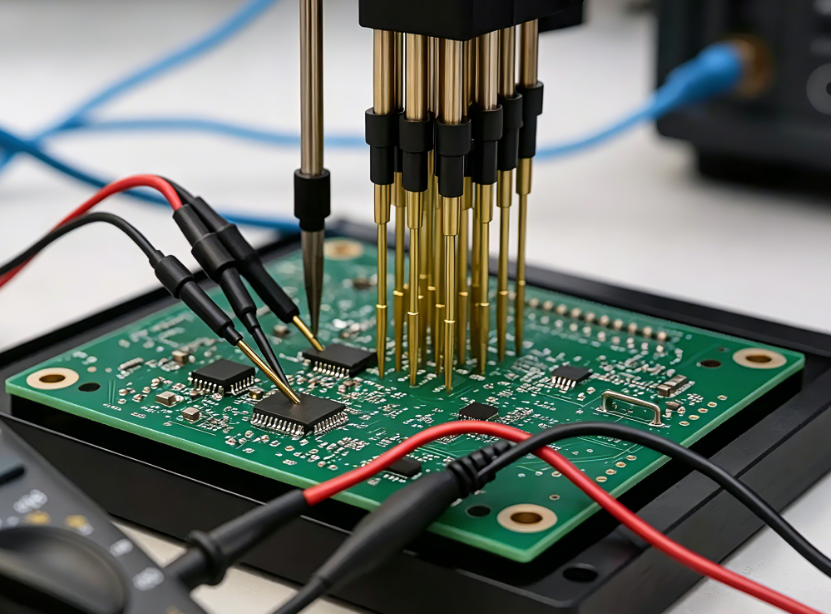
                  Q4: How do I choose between a lead frame package and a substrate package for my device?

                  A4: Choose a lead frame package if your device has low to mid pin counts (up to 200 pins), requires cost efficiency, and does not need an ultra compact footprint. Lead frame packages are ideal for consumer electronics, automotive, and industrial applications where reliability and thermal performance are important but high I/O density is not. Choose a substrate package if your device has high pin counts (200+ pins), requires a small footprint, or needs vertical chip stacking (e.g., high performance SoCs, wearables).

                  Q5: What is the typical cost of a lead frame package compared to a substrate package?

                  A5: Lead frame packages are significantly less expensive than substrate packages. On average, a lead frame package costs 30-70% less than a substrate package with similar pin counts. This cost difference is due to the simpler manufacturing process of lead frame packages, which uses standard equipment and materials. Substrate packages are more expensive because they require specialized manufacturing processes for the high density substrate.

                  Q6: Can lead frame packages be used in surface mount technology (SMT) applications?

                  A6: Yes, most modern lead frame packages are designed for surface mount technology (SMT) applications. SMT compatible lead frame packages (e.g., SOP, QFP, PLCC) have leads bent into gull wing or J shapes, which allow them to be soldered directly to the surface of the PCB. This eliminates the need for through holes, reducing the PCB size and enabling more compact device designs. Lead frame packages are widely used in SMT applications across consumer electronics, automotive, and industrial industries.

                  You may also like

                  Body Control Module: Functions, Testing, Failure Symptoms, and PCB Design Considerations

                  April 30th, 2026

                  A body control module is an electronic control unit that manages many comfort, convenience, lighting, access, and body-related functions in a vehicle. It does not usually control engine combustion or transmission shifting. Instead, it coordinates systems such as power windows, door locks, interior lights, exterior lights, wipers, keyless entry, alarm functions, and sometimes parts of climate control or immobilizer logic.

                  What Is a Body Control Module?

                  A body control module, often shortened to BCM, is a vehicle electronic control unit responsible for managing body electronics. It receives input signals from switches, sensors, remote keys, door modules, and other ECUs. Then it processes those signals and sends commands to actuators, lights, motors, locks, and other electrical loads.

                  For example, when a driver presses the lock button on a key fob, the BCM receives the signal, verifies the command, communicates with other modules if needed, and then activates the door lock circuit. When a door opens, the BCM may turn on the interior light, send a door-open message to the instrument cluster, and monitor whether the alarm system should respond.

                  In modern vehicles, the BCM is usually connected to communication networks such as CAN, LIN, or other in-vehicle buses.

                  What Is a Body Control Module?

                  What Does a Body Control Module Do?

                  A body control module controls and coordinates many electrical functions that drivers use every day. These functions may look simple from the outside, but they require stable signal processing, software logic, and reliable PCB-level power control inside the module.

                  Common BCM-controlled functions include:

                  Function AreaTypical BCM Role
                  LightingControls interior lamps, headlights, turn signals, brake lights, fog lamps, and courtesy lights
                  Door systemControls central locking, door ajar signals, trunk release, and sometimes power sliding doors
                  Window and mirror systemCoordinates power windows, mirror adjustment, mirror folding, and defrost signals
                  Wiper systemManages windshield wipers, washer pumps, and intermittent wiper timing
                  Security systemSupports anti-theft alarm, keyless entry, immobilizer communication, and remote control logic
                  Cabin convenienceControls seat memory, sunroof signals, interior dimming, and accessory power
                  Vehicle communicationSends and receives data from other ECUs through CAN, LIN, or similar networks

                  Instead of running separate hardwired circuits for every function, the vehicle can use network communication between modules. This improves design flexibility and allows more advanced features to be controlled through software.

                  What Is Inside a Body Control Module PCB?

                  Inside a body control module, the PCB is the foundation of the entire system. It provides mechanical support, electrical connection, signal routing, power distribution, grounding, thermal paths, and communication integrity.

                  A typical body control module PCB may include:

                  PCB/PCBA ElementFunction
                  Microcontroller unitProcesses input signals and runs BCM software logic
                  Power management ICsRegulate voltage for MCU, memory, communication circuits, and driver stages
                  CAN/LIN transceiversEnable communication with other vehicle control modules
                  MOSFETs or relay driversSwitch lamps, locks, motors, and other electrical loads
                  EEPROM or flash memoryStores configuration, vehicle coding, fault data, or learned settings
                  TVS diodes and ESD protectionProtect circuits from voltage spikes and electrostatic discharge
                  Crystal oscillatorProvides timing reference for the microcontroller
                  ConnectorsLink the BCM to vehicle wiring harnesses
                  Current sensing circuitsMonitor load condition, short circuits, or abnormal current
                  Relays or solid-state switchesControl higher-current body functions

                  The PCB inside a BCM often uses FR-4 or high-Tg FR-4 material, depending on thermal and reliability requirements. In higher-reliability designs, the manufacturer may need controlled impedance routing, wider copper traces for power paths, stronger solder joint reliability, and protective coating against moisture or contamination.

                  How Does the PCB in a Body Control Module Control Vehicle Electronics?

                  The PCB in a body control module works as the electrical and logical platform for the whole unit. It routes low-voltage signals from switches and sensors to the microcontroller. It also carries higher-current paths that drive lights, locks, motors, and relays.

                  The process usually works like this:

                  1. Input detection
                  A switch, sensor, key fob receiver, or another ECU sends a signal to the BCM.

                  2. Signal conditioning
                  The PCB circuit filters noise, protects against surge voltage, and converts the signal into a level the microcontroller can read.

                  3. Software decision
                  The microcontroller checks the command, vehicle status, safety logic, and stored configuration.

                  4. Output driving
                  The BCM activates a MOSFET, relay, or driver IC to control the required load.

                  5. Network feedback
                  The BCM may send status information to the instrument cluster, gateway, alarm system, or diagnostic tool.

                  Because of this workflow, BCM PCB design must balance signal integrity, power integrity, EMC protection, thermal performance, and connector durability. A weak PCB layout may lead to unstable signals, false triggers, communication errors, or early component failure.

                  What Components Are Used in a Body Control Module PCBA?

                  A body control module PCBA uses both signal-level and power-level components. The exact design depends on the vehicle platform, OEM requirements, and electrical architecture.

                  Common components include:

                  What Components Are Used in a Body Control Module PCBA?

                  Microcontroller
                  This is the main processing device. It runs firmware, reads input signals, controls outputs, manages diagnostics, and communicates with other modules.

                  CAN and LIN transceivers
                  These components allow the BCM to exchange information with the instrument cluster, door modules, gateway, engine ECU, HVAC module, and other control units.

                  MOSFETs and driver ICs
                  Many body loads require current switching. MOSFETs are often used for lamps, motors, solenoids, and lock actuators. Driver ICs improve control stability and protection.

                  Relays
                  Some BCM designs still use relays for certain high-current or isolated switching functions, although many newer designs use solid-state power devices.

                  Voltage regulators
                  The vehicle battery voltage is unstable compared with consumer electronics power rails. Regulators convert the input voltage into stable levels for ICs and logic circuits.

                  Protection devices
                  TVS diodes, ESD suppressors, fuses, current-limiting parts, and reverse-polarity protection are used to protect the PCBA from harsh automotive electrical events.

                  Connectors
                  BCM connectors must withstand vibration, insertion force, humidity, temperature cycling, and long-term vehicle use.

                  Passive components
                  Resistors, capacitors, inductors, and filters help stabilize signals, reduce noise, and support EMC performance.

                  For PCB assembly, component selection should consider AEC-Q qualification, temperature rating, traceability, long-term availability, and solder joint reliability.

                  Where Is the Body Control Module Located on a Car?

                  The body control module location depends on the vehicle brand, model, year, and architecture. It is commonly installed inside the cabin because it needs access to many interior wiring harnesses and body electronics.

                  Common BCM locations include:

                  Possible LocationWhy It Is Used
                  Under the dashboardClose to switches, instrument panel, and cabin wiring
                  Behind the glove boxProtected location with space for module mounting
                  Driver-side kick panelNear fuse box and body harness connections
                  Near the interior fuse boxEasy integration with power distribution
                  Center console areaConvenient for cabin electronics routing
                  Under a seatUsed in some vehicle platforms, but moisture protection becomes important

                  The exact location should always be checked in the vehicle service manual. Removing trim panels without correct guidance may damage connectors, clips, or wiring harnesses.

                  How to Test a Body Control Module?

                  Testing a body control module should be systematic. Many symptoms that look like a bad BCM may actually come from a weak battery, blown fuse, damaged wiring, poor ground, water ingress, or a failed actuator.

                  A practical BCM testing process includes:

                  1. Check the battery and charging system
                  Low voltage can cause communication errors, false warning lights, and intermittent BCM behavior.

                  2. Inspect fuses and relays
                  A blown fuse may disable one function and make the BCM appear faulty.

                  3. Scan for diagnostic trouble codes
                  A professional scan tool can read BCM-related DTCs, communication errors, input status, and output commands.

                  4. Check power and ground at the BCM connector
                  The BCM needs stable battery feed, ignition feed, and ground. Voltage drop testing is useful here.

                  5. Inspect connectors and wiring harnesses
                  Look for corrosion, loose pins, bent terminals, water marks, burnt areas, or previous repair damage.

                  6. Test input and output functions
                  Use a scan tool to monitor switch inputs and command outputs such as locks, lights, and wipers.

                  7. Check network communication
                  CAN or LIN communication problems can make the BCM lose contact with other modules.

                  8. Confirm software coding or programming
                  Some BCMs need vehicle-specific programming after replacement. An unprogrammed module may not work correctly even if the hardware is good.

                  What Testing Is Required for Body Control Module PCB Assembly?

                  For body control module PCBA manufacturing, testing must be much more rigorous than ordinary consumer electronics testing. Automotive electronics operate under vibration, electrical noise, temperature variation, humidity, and long service life expectations.

                  Common BCM PCBA testing may include:

                  Test MethodPurpose
                  AOI inspectionChecks solder joints, component placement, polarity, and missing parts
                  X-ray inspectionInspects hidden solder joints under QFN, BGA, or other bottom-terminated components
                  ICT testVerifies circuit connectivity, resistance, capacitance, and basic component values
                  Functional testConfirms actual BCM input, output, communication, and control behavior
                  Programming testLoads firmware and verifies successful MCU programming
                  CAN/LIN communication testConfirms stable vehicle network communication
                  High-low temperature testEvaluates operation under automotive temperature stress
                  Burn-in testScreens early-life failures before shipment
                  Vibration-related validationHelps verify solder joint and connector durability
                  Conformal coating inspectionConfirms coating coverage and protects against moisture or contamination

                  A body control module PCB assembly should also follow strict traceability. Component lot numbers, PCB batch data, process records, test results, and repair history should be documented. This is especially important for automotive projects that require IATF 16949-based quality management.

                  What Causes a BCM to Fail?

                  A BCM can fail due to electrical, mechanical, environmental, software, or manufacturing-related factors. Since the BCM connects to many circuits, it is exposed to more risk than a simple single-function module.

                  Common causes include:

                  Water ingress
                  Moisture can corrode connectors, damage PCB traces, create leakage paths, and cause intermittent faults.

                  Voltage spikes
                  Load dump, jump-start mistakes, alternator problems, or poor grounding can create harmful voltage transients.

                  Short circuits in connected loads
                  A shorted lock actuator, lamp circuit, motor, or harness may overload BCM output drivers.

                  Connector corrosion
                  Even if the PCB is intact, poor connector contact can interrupt signals or power supply.

                  Solder joint fatigue
                  Thermal cycling and vibration can weaken solder joints over time, especially around large components and connectors.

                  PCB contamination
                  Flux residue, ionic contamination, or poor cleaning can reduce insulation resistance and create leakage issues.

                  Software or programming issues
                  Incorrect coding, failed updates, or incompatible replacement modules can cause abnormal behavior.

                  Manufacturing defects
                  Poor soldering, weak component placement, insufficient inspection, or unqualified components may shorten service life.

                  For PCB manufacturers, these failure causes show why automotive PCBA needs strong process control, stable materials, and complete test coverage.

                  What Are Common PCB Failure Points in a Body Control Module?

                  Inside a body control module, several PCB areas are more vulnerable than others because they handle current, heat, vibration, or external wiring stress.

                  Common PCB failure points include:

                  Failure PointPossible Result
                  Connector solder jointsIntermittent power, ground, or signal loss
                  MOSFET output stageFailed lights, locks, wipers, or motor control
                  Power regulation areaNo communication, random reset, or complete module failure
                  CAN/LIN transceiver circuitCommunication loss with other ECUs
                  Protection componentsReduced surge protection after severe electrical events
                  Ground plane or power traceVoltage drop, heating, or unstable operation
                  Relay solder jointsIntermittent output control
                  Contaminated PCB surfaceLeakage current, false input signal, or corrosion

                  Many BCM failures are not caused by the microcontroller itself. They often come from power supply instability, corroded connectors, damaged output drivers, poor solder joints, or PCB contamination.

                  What Happens When the Body Control Module Goes Bad?

                  When the body control module goes bad, the vehicle may show multiple electrical symptoms at the same time. Since the BCM manages many body functions, failure symptoms can appear unrelated at first.

                  Common bad BCM symptoms include:

                  • Power windows stop working or behave inconsistently
                  • Door locks fail, cycle randomly, or do not respond to the key fob
                  • Interior lights stay on, flicker, or fail to turn on
                  • Headlights, turn signals, or brake lights act abnormally
                  • Windshield wipers work at the wrong speed or fail to park correctly
                  • Alarm system triggers unexpectedly
                  • Keyless entry stops working
                  • Instrument cluster shows warning messages
                  • Battery drains overnight due to a module staying awake
                  • Vehicle fails to recognize the key in some systems
                  • Communication codes appear during scan tool diagnosis

                  One important point: these symptoms do not always prove the BCM itself is defective. A wiring fault, water-damaged connector, weak battery, or failed actuator can create similar problems. Proper diagnosis should come before replacement.

                  Why Is PCB Design Important for Body Control Module Reliability?

                  PCB design is critical in a body control module because the board must manage low-level logic signals and higher-current body loads in the same assembly. It must also survive automotive electrical noise, heat, humidity, vibration, and long working cycles.

                  Important BCM PCB design considerations include:

                  Power integrity
                  The PCB must distribute stable voltage to the microcontroller, communication ICs, memory, and output stages. Poor power routing may cause resets or unstable logic.

                  Grounding strategy
                  A strong ground design reduces noise, improves EMC behavior, and keeps sensing circuits stable.

                  Thermal design
                  MOSFETs, voltage regulators, and relays can generate heat. Copper area, thermal vias, and component spacing help control temperature rise.

                  EMC and EMI control
                  BCM circuits must avoid generating excessive interference and must resist external electromagnetic noise.

                  Protection design
                  Automotive PCBs need protection against ESD, surge, reverse polarity, load dump, and transient voltage events.

                  Connector reinforcement
                  Connectors face mechanical stress from harness movement and vibration. PCB pad design and solder joint quality are important.

                  Moisture protection
                  Conformal coating, solder mask quality, enclosure design, and cleanliness help reduce corrosion and leakage current.

                  A reliable BCM PCB is not only about connecting components. It is about creating a stable electrical platform for the complete vehicle body control system.

                  Body Control Module PCB

                  How Does Automotive PCBA Manufacturing Affect BCM Performance?

                  Automotive PCBA manufacturing has a direct influence on BCM performance because small process variations can become long-term reliability risks.

                  For example, insufficient solder paste may cause weak solder joints. Excessive voiding under power components may increase thermal resistance. Poor cleaning may leave ionic contamination on the PCB surface. Uncontrolled component sourcing may introduce parts with inconsistent quality or uncertain traceability.

                  For BCM projects, a capable automotive PCBA manufacturer should provide:

                  • Automotive-grade component sourcing
                  • PCB fabrication with stable material control
                  • Accurate SMT placement
                  • AOI and X-ray inspection
                  • Reflow profile control
                  • ICT and functional testing
                  • Firmware programming support
                  • Conformal coating when required
                  • Full traceability for components, PCB batches, and process data
                  • Engineering support for DFM, DFA, and DFT review

                  For vehicle electronics, the PCBA must be manufactured as a controlled engineering product, not just assembled as a common circuit board. This is especially important for BCMs because they connect to many user-facing and safety-adjacent vehicle functions.

                  How Much Does a BCM Cost to Replace?

                  The cost to replace a body control module depends on the vehicle model, module type, labor rate, programming requirement, and whether the part is new, remanufactured, or used. As a general market reference, RepairPal estimated the average BCM replacement cost at $666 to $725, with labor estimated at $115 to $169 and parts around $551 to $556. RepairPal also lists body control system diagnosis and testing at $49 to $72 on average. These ranges do not include taxes, fees, location differences, or related repairs.

                  How Do I Reset the Body Control Module?

                  A body control module reset may help in some cases, especially when the issue is caused by temporary software lockup or low-voltage confusion. However, resetting the BCM will not repair damaged hardware, corroded connectors, shorted circuits, or failed PCB components.

                  Common reset methods may include:

                  Battery disconnect reset
                  Some technicians disconnect the negative battery terminal for a period of time, then reconnect it. This may clear temporary module states in some vehicles.

                  Scan tool reset
                  A professional diagnostic tool may perform a BCM reset, relearn, or initialization procedure.

                  Fuse removal reset
                  In some vehicles, removing the BCM fuse for a short time may reset the module. This must be done according to the service manual.

                  Software relearn or programming
                  After replacement, the BCM may require coding, programming, immobilizer relearn, or key matching.

                  Before resetting a BCM, it is better to record diagnostic trouble codes. Clearing or resetting the module too early may erase useful diagnostic information.

                  For modern vehicles, always follow the OEM service procedure. Incorrect reset or programming may create more electrical problems.

                  How to Choose a Reliable Body Control Module PCB Manufacturer?

                  Choosing a reliable body control module PCB manufacturer requires more than checking price and lead time. BCM electronics are used in a demanding automotive environment, so the supplier should understand both PCB fabrication and automotive PCBA requirements.

                  A good BCM PCB or PCBA supplier should offer:

                  Selection FactorWhy It Matters
                  Automotive experienceHelps avoid design and process risks specific to vehicle electronics
                  IATF 16949 quality mindsetSupports automotive process control and traceability
                  DFM reviewFinds PCB manufacturability issues before production
                  DFT supportImproves test coverage and reduces hidden defects
                  Component traceabilityReduces counterfeit and lifecycle risks
                  Functional testing capabilityVerifies real BCM behavior before shipment
                  Conformal coating processImproves moisture and contamination resistance
                  Engineering communicationHelps solve layout, material, thermal, and assembly problems faster

                  For BCM PCB projects, EBest PCB can support PCB fabrication, component sourcing, PCBA assembly, inspection, functional testing coordination, and engineering review. This is useful for automotive electronics teams that need one supplier to manage both circuit board quality and assembly reliability.

                  FAQs About Body Control Module

                  1. What is a body control module in simple words?

                  A body control module is a vehicle computer that controls many electrical body functions, such as lights, door locks, windows, wipers, keyless entry, and alarm systems.

                  2. Is the BCM the same as the ECU?

                  No. The BCM is one type of ECU, but it is not usually the engine ECU. The engine ECU controls engine operation, while the BCM controls many body and cabin electronics.

                  3. Can a bad BCM drain the battery?

                  Yes. A faulty BCM may keep circuits awake when the vehicle is parked. This can create parasitic current draw and drain the battery overnight.

                  4. Can a BCM be repaired instead of replaced?

                  Sometimes, yes. If the issue is caused by a damaged relay, solder joint, connector, or power component, repair may be possible. However, many professional workshops replace and program the module for reliability and warranty reasons.

                  5. Does a used BCM need programming?

                  In many vehicles, yes. A used BCM may need coding, immobilizer matching, key relearn, or software configuration before it works correctly.

                  6. What PCB material is used in a body control module?

                  Many BCM PCBs use automotive-grade FR-4 or high-Tg FR-4. The final material depends on thermal requirements, reliability targets, copper weight, operating environment, and OEM specifications.

                  7. Why does a BCM PCB need conformal coating?

                  Conformal coating helps protect the PCB against moisture, dust, flux residue risk, and corrosion. It is especially useful when the module may be exposed to humidity or condensation.

                  8. What is the most common BCM failure symptom?

                  There is no single symptom for all vehicles. Common signs include abnormal lights, failed locks, keyless entry problems, wiper issues, communication codes, and unexplained battery drain.

                  You may also like

                  How to Identify Electronic Components on a Circuit Board?

                  April 29th, 2026

                  Have you ever stared at a circuit board and wondered how to accurately recognize the tiny parts that power every electronic device? Circuit board electronic components are the building blocks of all modern electronics, and knowing how to identify them correctly is critical for troubleshooting, maintenance, and accurate analysis. This guide breaks down every essential step, from distinguishing different component types to reading markings, testing functionality, and protecting these parts, all with practical, actionable advice to solve common pain points and avoid costly mistakes.

                  How to Identify Electronic Components on a Circuit Board, https://www.bestpcbs.com/blog/2026/04/how-to-identify-electronic-components-on-a-circuit-board/

                  What Are the Electronic Components of a Circuit Board?

                  Electronic circuit board components are discrete parts that work together to enable the circuit’s functionality, each serving a specific electrical purpose. These components fall into two main categories: passive and active, with additional specialized types that support overall performance.

                  Passive components do not require external power to operate and are essential for regulating electrical signals. The most common passive components include resistors, which limit current flow and divide voltage; capacitors, which store and release electrical charge to filter noise and stabilize power; inductors, which store energy in magnetic fields and suppress voltage spikes; and diodes, which allow current to flow in only one direction. These components are found on every circuit board and form the foundation of basic circuit operation.

                  Active components require external power to function and can amplify signals or switch current. Transistors are key active components, used to amplify electrical signals and act as switches in digital circuits. Integrated circuits (ICs) are complex active components that pack hundreds or thousands of miniaturized components into a single chip, serving as the “brain” of the circuit for processing, control, or memory storage. Other active components include LEDs, which emit light when current passes through them, and relays, which switch high-power circuits using low-power signals.

                  Additional specialized components include fuses, which protect the circuit from overcurrent by melting and breaking the circuit; connectors, which link the circuit board to external devices or other boards; and switches, which control the flow of current by opening or closing the circuit. Together, these components form a cohesive system that enables the circuit board to perform its intended function, making circuit board electronic components indispensable to all electronic devices.

                  How to Distinguish Surface Mount and Through-Hole Circuit Board Electronic Components?

                  Distinguishing surface mount and through-hole circuit board electronic components is straightforward once you know their key physical and mounting characteristics. Both types serve the same electrical purposes but differ in design, mounting method, and application, with clear visual cues to tell them apart.

                  • Mounting Method: Surface mount components (SMDs) are soldered directly to the surface of the circuit board, with small terminals or pads that attach to copper traces on the board’s top or bottom. Through-hole components have long metal leads that pass through holes drilled in the circuit board, with soldering done on the opposite side of the board to secure the component.
                  • Size and Shape: Surface mount components are significantly smaller and flatter than through-hole components. They come in compact rectangular, square, or chip-like shapes, with no protruding leads (or very short leads). Through-hole components are larger, with cylindrical or rectangular bodies and long, thin leads that extend outward from the component.
                  • Lead Configuration: Surface mount components have leads or pads along their edges or bottom, designed to sit flush against the circuit board. Through-hole components have one or more leads that extend straight out from the component body, intended to be inserted through pre-drilled holes in the board.
                  • Visual Cues: Surface mount components often appear as tiny “chips” on the board’s surface, with no leads visible through the board. Through-hole components have leads that pass through the board, with solder joints visible on the opposite side. Older circuit boards typically use more through-hole components, while modern, compact devices rely primarily on surface mount components.
                  • Application Context: Surface mount components are used in compact devices like smartphones, laptops, and wearables, where space is limited. Through-hole components are used in applications requiring high mechanical strength, such as industrial equipment, power supplies, and prototyping, where manual assembly and durability are prioritized.

                  How to Identify Electronic Components on a Circuit Board?

                  Identifying electronic components on a circuit board involves a combination of visual inspection, reading silk screen markings, and understanding component characteristics. Follow these step-by-step methods to accurately identify any component, even on dense or complex boards.
                  • Check Silk Screen Markings: Most circuit boards have a silk screen layer white or gray printed text and symbols that labels each component. These labels use standard abbreviations to indicate the component type: R for resistor, C for capacitor, D for diode, Q for transistor, U for integrated circuit, L for inductor, F for fuse, and SW for switch. The label (e.g., R12, C5, U3) corresponds to the component’s position in the circuit schematic, making identification quick and accurate.
                  • Recognize Physical Characteristics: Each component type has distinct physical features. Resistors are small, cylindrical (through-hole) or rectangular (surface mount) with color bands or numerical codes. Capacitors are round (electrolytic), flat (ceramic), or rectangular (film) and may have voltage or capacitance markings. Diodes have a stripe on one end indicating the cathode (negative terminal). Integrated circuits are black chips with multiple legs or pads, often with a small dot or notch marking pin 1.
                  • Use Component Markings: Most components have printed markings that indicate their values, ratings, or part numbers. Resistors use color bands or 3-4 digit codes to show resistance and tolerance. Capacitors use numerical codes (e.g., 104 = 100,000 picofarads) or direct markings for capacitance and voltage. Transistors and ICs have part numbers that can be looked up to confirm their type and specifications.
                  • Verify with a Multimeter: For uncertain components, use a multimeter to test electrical properties. Resistors can be tested for resistance, capacitors for capacitance, diodes for forward/reverse bias, and transistors for continuity between pins. This step confirms the component’s type and functionality, ensuring accurate identification.
                  • Cross-Reference with Schematics: If available, use the circuit board’s schematic diagram or bill of materials (BOM) to cross-reference component labels. Schematics show the component’s role in the circuit, while the BOM lists exact part numbers and specifications, eliminating guesswork.

                  How to Read the Markings and Codes on Circuit Board Electronic Components?

                  Markings and codes on circuit board electronic components provide critical information about their specifications, including value, tolerance, voltage rating, and functionality. Reading these codes correctly is essential for identifying components and ensuring they meet the circuit’s requirements, with standardized formats for each component type.

                  • Resistor Markings: Through-hole resistors use color bands to indicate resistance and tolerance. The first two bands are the significant digits, the third band is the multiplier, and the fourth band (if present) is the tolerance. Surface mount resistors use 3 or 4-digit codes: 3-digit codes have two significant digits and one multiplier (e.g., 102 = 10 x 10² = 1,000 ohms), while 4-digit codes have three significant digits and one multiplier (e.g., 1002 = 100 x 10² = 10,000 ohms). Tolerance is often marked with a letter: J = ±5%, K = ±10%, M = ±20%.
                  • Capacitor Markings: Capacitor markings vary by type and size. Large electrolytic capacitors directly print capacitance (e.g., 10µF) and voltage (e.g., 25V) on the body. Small surface mount capacitors use 2 or 3-digit codes: the first two digits are significant, the third is the multiplier (in picofarads), with no decimal point (e.g., 104 = 10 x 10⁴ = 100,000 pF = 100 nF). Some capacitors use letters to indicate tolerance, with J = ±5% and K = ±10% being common.
                  • Diode Markings: Diodes have a single stripe on one end, which marks the cathode (negative terminal). Some diodes also have part numbers printed on the body (e.g., 1N4001), which can be looked up to confirm their type (e.g., rectifier diode) and voltage/current ratings. LEDs have a similar stripe for the cathode, with additional color markings to indicate the light color.
                  • Transistor Markings: Transistors have alphanumeric part numbers (e.g., 2N2222, BC547) printed on the body. These part numbers identify the transistor type (NPN, PNP) and specifications like current, voltage, and gain. Some transistors also have a dot or notch to indicate the collector, base, or emitter pin.
                  • Integrated Circuit (IC) Markings: ICs have a part number (e.g., ATmega328P, LM358) printed on the top, which identifies the chip’s functionality (e.g., microcontroller, operational amplifier). A small dot or notch on the IC marks pin 1, which is critical for proper orientation when installing or testing the component. Some ICs also include manufacturer logos or date codes.

                  What Tools Are Needed to Identify Electronic Circuit Board Components Accurately?

                  Accurate identification of electronic circuit board components requires a few essential tools, designed to enhance visibility, measure electrical properties, and verify component functionality. These tools are affordable, easy to use, and critical for avoiding misidentification and costly errors.

                  • Magnifying Glass or Digital Microscope: Most circuit board electronic components are tiny, with small markings that are difficult to read with the naked eye. A magnifying glass (1020x magnification) works for basic inspection, while a digital microscope provides higher magnification and allows for detailed viewing of small surface mount components and fine markings.
                  • Digital Multimeter: A multimeter is the most versatile tool for component identification. It measures resistance (for resistors), capacitance (for capacitors), voltage (for diodes and ICs), and continuity (for testing component leads). Look for a multimeter with auto-ranging functionality for ease of use, as it automatically selects the correct measurement range.
                  • Component Tester: A dedicated component tester quickly identifies resistors, capacitors, diodes, transistors, and inductors by measuring their key parameters and displaying the component type and value. This tool eliminates guesswork, especially for unmarked surface mount components.
                  • Gerber Viewer Software: Gerber files are used to design circuit boards, and Gerber viewer software allows users to visualize the board’s layers, component footprints, and silk screen markings. This tool helps cross-reference component labels with their physical positions on the board, useful for complex or dense circuits.
                  • Soldering Iron and Desoldering Tool: For components that need to be removed for closer inspection or testing, a soldering iron (2530W for surface mount, 4060W for through-hole) and desoldering tool (solder sucker or desoldering braid) are essential. These tools allow safe removal of components without damaging the circuit board or the component itself.
                  • Flashlight or Task Light: Proper lighting is critical for visual inspection. A bright, focused flashlight or task light illuminates small components and markings, making it easier to read silk screen labels and component codes, especially on dark or densely populated circuit boards.

                  How to Identify Faulty Circuit Board Electronic Components During Identification?

                  Identifying faulty circuit board electronic components during inspection involves recognizing visual signs of damage and using tools to test functionality. Faulty components often show clear physical indicators, and simple tests can confirm whether a component is working correctly, saving time in troubleshooting.

                  • Visual Inspection for Physical Damage: Look for obvious signs of damage, such as burnt or discolored components (common in resistors and ICs), bulging or leaking capacitors (electrolytic capacitors often bulge when faulty), cracked component bodies, or broken leads. These visual cues indicate a faulty component that needs replacement.

                  • Test for Continuity: Use a multimeter in continuity mode to check for broken leads or internal damage. A component with broken leads will show no continuity, while a faulty resistor or diode may show inconsistent continuity. For example, a diode should show continuity in one direction only; continuity in both directions indicates a faulty diode.
                  • Measure Component Values: Compare the measured value of a component to its marked value. A resistor with a measured resistance significantly higher or lower than its marked value is faulty. A capacitor with a measured capacitance below 80% of its marked value is likely faulty and should be replaced.
                  • Check for Overheating: During operation, touch components (carefully to avoid burns) to feel for excessive heat. Components that are abnormally hot (beyond their normal operating temperature) are likely faulty, as overheating indicates internal damage or incorrect operation.
                  • Inspect Solder Joints: Faulty solder joints (cold solder, bridging, or poor adhesion) can cause components to function incorrectly. Look for solder joints that are dull, cracked, or not fully covering the component lead and circuit board pad. These joints can be reflowed with a soldering iron to restore connectivity.
                  • Cross-Reference with Circuit Behavior: If the circuit is not functioning as intended, cross-reference the component’s role in the schematic with the observed behavior. For example, a non-functional LED may indicate a faulty resistor (limiting current) or a faulty LED itself. Testing the component’s value will confirm which is faulty.
                  Circuit board electronic components, https://www.bestpcbs.com/blog/2026/04/how-to-identify-electronic-components-on-a-circuit-board/

                  How to Test Electronic Components on a Circuit Board?

                  Testing electronic components on a circuit board ensures they function correctly and meet the circuit’s specifications. The testing process varies by component type but follows a consistent, step-by-step approach using basic tools, with clear pass/fail criteria for each component.

                  • Resistor Testing: Set the multimeter to resistance mode (ohms). Touch the multimeter probes to the resistor’s leads (no need to remove the resistor from the board if it is not in parallel with other components). Compare the measured resistance to the resistor’s marked value. A measured value within the component’s tolerance (±5%, ±10%, or ±20%) indicates a working resistor; a value outside this range means the resistor is faulty.
                  • Capacitor Testing: Set the multimeter to capacitance mode. For large electrolytic capacitors, discharge them first (use a resistor to discharge stored charge). Touch the probes to the capacitor’s terminals (match positive to positive, negative to negative for polarized capacitors). A measured capacitance within 10-20% of the marked value is acceptable; values significantly lower indicate a faulty capacitor.
                  • Diode Testing: Set the multimeter to diode mode. Touch the positive probe to the diode’s anode (no stripe) and the negative probe to the cathode (stripe). A working diode will show a voltage drop (0.5-0.7V for silicon diodes). Reverse the probes, no voltage drop should be displayed. If voltage is displayed in both directions or no voltage is displayed in either direction, the diode is faulty.
                  • Transistor Testing: For NPN transistors, set the multimeter to diode mode. Touch the positive probe to the base and the negative probe to the emitter, this should show a voltage drop. Touch the positive probe to the base and the negative probe to the collector, another voltage drop should be displayed. Reverse the probes for PNP transistors. No voltage drop in either test indicates a faulty transistor.
                  • Integrated Circuit (IC) Testing: Testing ICs requires a multimeter and knowledge of the chip’s pinout (from the datasheet). Measure the voltage at the power pins (VCC and GND) to ensure the IC is receiving power. Check the output pins against the expected voltage (from the schematic). If the IC is not receiving power or the output is incorrect, the IC is likely faulty. For more detailed testing, use an IC tester or oscilloscope.
                  • Inductor Testing: Set the multimeter to resistance mode. Touch the probes to the inductor’s leads. A working inductor will show low resistance (near zero ohms). High resistance or no continuity indicates a broken inductor coil, which is faulty.
                  Circuit Board Electronic Components, https://www.bestpcbs.com/blog/2026/04/how-to-identify-electronic-components-on-a-circuit-board/

                  How to Remove Electronic Components from a Circuit Board?

                  Removing electronic components from a circuit board requires care to avoid damaging the board, the component (if reuse is needed), and surrounding components. The process varies slightly for surface mount and through-hole components, but follows consistent best practices to ensure safe removal.

                  • Prepare the Workspace: Ensure the circuit board is disconnected from power and any external devices. Use an anti-static mat and anti-static wristband to prevent electrostatic discharge (ESD) damage to sensitive components. Gather the necessary tools: soldering iron, desoldering tool (solder sucker or desoldering braid), tweezers, and a magnifying glass.
                  • Removing Through-Hole Components: Heat the solder joint on one lead of the component with the soldering iron. Once the solder melts, use the desoldering sucker to remove the molten solder. Repeat for the other lead(s). Once all solder is removed, gently pull the component’s leads through the board using tweezers. If solder remains in the holes, use the desoldering braid to remove it.
                  • Removing Surface Mount Components: Use a soldering iron with a fine tip or a hot air station (preferred for small components). For components with multiple leads (e.g., ICs), heat all leads simultaneously with the hot air station (set to 300350°C) until the solder melts. For single-lead components (e.g., resistors, capacitors), heat one lead at a time, using tweezers to lift the component once the solder melts. Avoid applying excessive heat, as this can damage the circuit board’s copper traces.
                  • Clean the Solder Pads: After removing the component, use desoldering braid to clean any remaining solder from the circuit board’s pads. This ensures the pads are flat and free of debris, making it easier to install a new component if needed.
                  • Inspect for Damage: After removal, inspect the circuit board for damaged copper traces or pads. If a trace is lifted or damaged, use a soldering iron to reattach it (if possible) or use a jumper wire to restore connectivity. Inspect the removed component for damage if reuse is intended.
                  • Handle Components Carefully: Use tweezers to handle components, avoiding direct contact with the leads or pins. This prevents ESD damage and contamination from oils on the hands, which can affect component performance.

                  How to Avoid Damaging Circuit Board Electronic Components During Identification?

                  Damaging circuit board electronic components during identification is a common mistake that can lead to costly repairs or component failure. Following these simple steps ensures components and the circuit board remain intact during inspection, testing, and handling.

                  • Use Anti-Static Protection: Electrostatic discharge (ESD) can damage sensitive components like ICs and transistors. Always use an anti-static mat and anti-static wristband when handling the circuit board and components. Avoid touching component pins or leads directly with bare hands, as oils and static can cause damage.
                  • Avoid Excessive Heat: When using a soldering iron or hot air station, set the temperature to the minimum required (300350°C for surface mount components, 4060°C for through-hole). Excessive heat can melt component bodies, damage circuit board traces, or cause internal component failure. Limit heat exposure to 510 seconds per solder joint.
                  • Use the Right Tools: Avoid using sharp tools (e.g., screwdrivers, knives) to pry components, as this can damage leads, pins, or circuit board pads. Use tweezers with fine tips for handling small components, and a magnifying glass to avoid accidental contact with surrounding components.
                  • Do Not Force Components: If a component does not lift easily after desoldering, do not force it. Reheat the solder joints to ensure all solder is melted, and check for any hidden solder bridges that may be holding the component in place. Forcing components can break leads or lift copper traces.
                  • Discharge Capacitors Before Testing: Capacitors store electrical charge even after the circuit is disconnected from power. Discharge them using a resistor (1k10k ohms) before testing or removing them, as stored charge can cause electric shock or damage to the multimeter.
                  • Keep the Workspace Clean: A cluttered workspace increases the risk of dropping tools or components onto the circuit board, causing physical damage. Keep tools organized and the workspace free of debris, and use a soft mat to place the circuit board on to prevent scratches.
                  Circuit board electronic components, https://www.bestpcbs.com/blog/2026/04/how-to-identify-electronic-components-on-a-circuit-board/

                  How to Protect Electronic Components on a Circuit Board?

                  Protecting electronic components on a circuit board ensures long-term reliability and prevents damage from environmental factors, ESD, and physical wear. Proper protection methods vary by application but focus on shielding components from harm while maintaining their functionality.

                  • Apply Conformal Coating: Conformal coating is a thin, protective layer applied to the circuit board and components to shield them from moisture, dust, chemicals, and temperature variations. Common coating materials include acrylic (easy to remove, good for general protection), silicone (excellent heat resistance), and polyurethane (high chemical resistance). The coating is applied evenly, covering all components without blocking connectors or heat sinks.
                  • Use Heat Sinks: Components that generate significant heat (e.g., ICs, power transistors) require heat sinks to dissipate heat and prevent overheating. Heat sinks are attached to the component’s body using thermal paste, which improves heat transfer. Choose a heat sink size appropriate for the component’s power dissipation to ensure effective cooling.
                  • Implement ESD Protection: Install ESD protection components (e.g., TVS diodes, varistors) on the circuit board to divert static charge away from sensitive components. Use anti-static packaging for components during storage and transportation, and ensure the circuit board is grounded during assembly and operation.
                  • Protect Against Overcurrent and Overvoltage: Use fuses or circuit breakers to protect components from overcurrent, which can cause overheating and damage. Install voltage regulators or Zener diodes to prevent overvoltage, which can destroy sensitive components like ICs and transistors. These components act as a safety net, breaking the circuit or regulating voltage when limits are exceeded.
                  • Secure Components with Potting Compound: For circuit boards used in harsh environments (e.g., industrial, automotive), potting compound is poured over the board and components to provide complete protection from moisture, vibration, and physical damage. Potting compound is a rigid or flexible material that encapsulates the board, forming a protective barrier.
                  • Proper Storage and Handling: Store circuit boards in a dry, cool environment, away from direct sunlight and moisture. Use anti-static bags for individual boards or components, and avoid stacking boards to prevent physical damage. When handling, use anti-static protection and avoid touching component pins or leads.

                  FAQs About Electronic Components on a Circuit Board

                  Q1: Can I identify circuit board electronic components without removing them from the board?

                  A1: Yes, most circuit board electronic components can be identified without removal. Use silk screen markings to determine component type, visual cues to recognize physical characteristics, and a multimeter to test electrical properties. For unmarked components, use a component tester or cross-reference with the circuit schematic to confirm identification.

                  Q2: Why do some surface mount components have no markings?

                  A2: Small surface mount components (e.g., 0402 or 0201 size resistors and capacitors) often have no markings due to their tiny size. Manufacturers mark the reels holding these components instead of individual parts. To identify unmarked surface mount components, use a component tester to measure their values or cross-reference with the circuit’s BOM or schematic.

                  Q3: How do I know if a capacitor on a circuit board is faulty?

                  A3: Faulty capacitors often show visual signs like bulging, leaking, or discoloration. To confirm, use a multimeter to measure capacitance. A capacitor with a measured value below 80% of its marked value is faulty. Additionally, capacitors that overheat during operation or cause circuit malfunctions (e.g., voltage fluctuations) are likely faulty and should be replaced.

                  Q4: What is the difference between passive and active electronic circuit board components?

                  A4: Passive components do not require external power to operate and include resistors, capacitors, inductors, and diodes. They regulate electrical signals but do not amplify or switch current. Active components require external power and include transistors, ICs, LEDs, and relays. They amplify signals, switch current, or perform complex processing tasks.

                  Q5: How can I avoid ESD damage when working with circuit board electronic components?

                  A5: To avoid ESD damage, use an anti-static mat and anti-static wristband to ground yourself and the circuit board. Avoid touching component pins or leads with bare hands, and store components in anti-static bags. Ensure the workspace is free of static-generating materials (e.g., plastic, fabric) and ground all tools used during inspection and testing.

                  You may also like

                  How Much Gold in Circuit Boards? Identify Gold Circuit Board Gold in Electronics​

                  April 29th, 2026

                  In PCB manufacturing, the amount of gold in circuit boards is usually described by gold plating thickness, not by weight. For common ENIG surface finish, the immersion gold layer is typically about 1–3 µin thick, equal to 0.025–0.075 µm. For gold fingers, edge connectors, RAM contacts, and high-reliability plug-in areas, the gold is usually thicker, often around 15–30 µin, and some demanding designs may use 30–50 µin hard gold plating.

                  How Much Gold in Circuit Boards?

                  How Much Gold in Circuit Boards?

                  Do All Circuit Boards Have Gold?

                  Not all circuit boards have gold. Some do, some do not, and many contain only very small plated areas. Gold is usually applied only where the design needs stable contact performance, strong resistance to oxidation, or reliable signal transmission over time.

                  In practical PCB manufacturing, gold is not a default finish for every board. It is a selective engineering choice. Low-cost consumer products often use finishes such as HASL, OSP, immersion tin, or immersion silver instead. These options are cheaper and work well enough for many standard applications.

                  Gold is most commonly found in:

                  • edge connectors
                  • card fingers
                  • switch contacts
                  • socket interfaces
                  • high-reliability contact pads
                  • wire bonding areas in certain semiconductor packages

                  So, if someone asks, “Do all circuit boards have gold?” the best answer is simple: no, but many important electronic assemblies use gold in specific functional locations.

                  Is There Real Gold in Circuit Boards or Just Gold-Colored Coating?

                  Yes, the gold used in electronics is real gold. In most cases, however, it is a very thin plated layer rather than a thick deposit or solid piece of metal.

                  This distinction matters. When people see bright yellow connector fingers on a RAM module or motherboard slot, they often imagine a large amount of recoverable precious metal. In reality, that visible gold surface is usually only a thin functional coating applied over nickel. The nickel acts as a barrier and structural layer. The gold provides a clean, oxidation-resistant surface with excellent conductivity.

                  Common PCB-related gold finishes include:

                  Gold Finish TypeTypical UseWhy It Is UsedValue for Recovery
                  ENIGPCB pads and solderable surfacesFlatness, solderability, corrosion resistanceLow
                  Hard GoldEdge connectors, contact fingersWear resistance, repeated insertion cyclesMedium
                  Gold Bonding SurfacesSemiconductor packagingHigh-reliability interconnectionHigher
                  Thick Gold in Legacy PartsOlder CPUs and telecom hardwareLong-term durabilityHigher

                  So the answer is not “fake gold” versus “real gold.” It is usually real gold, but used in very small engineered quantities.

                  Where Is Gold Usually Found on a Circuit Board?

                  Gold is typically found in the places where contact quality matters most. That means it is not spread evenly across the whole board. It is concentrated in small functional areas.

                  The most common gold-bearing PCB areas include:

                  • connector fingers on memory modules and add-in cards
                  • contact pads in sockets and plug-in interfaces
                  • plated contacts in telecom and server boards
                  • switch contacts in precision electronics
                  • bonding pads in hybrid or semiconductor assemblies

                  A typical motherboard may have gold in the PCIe slots, RAM slot contacts, CPU socket areas, and selected chip connections. A standard low-cost appliance control board may have almost none.

                  Where Is Gold Usually Found on a Circuit Board?

                  How to Identify Gold in Electronics Without Guessing?

                  The fastest way to identify likely gold-bearing parts is visual inspection, but visual inspection alone is not enough for a confident conclusion. Gold color can be misleading. Some finishes look similar even when no gold is present.

                  A practical identification approach starts with observation:

                  • bright yellow metallic finish
                  • smooth, uniform contact surfaces
                  • no obvious tarnishing
                  • presence on connector fingers or high-contact pads
                  How to Identify Gold in Electronics Without Guessing?

                  Which Electronics Contain the Most Gold?

                  Not all electronics contain the same amount of gold. Older high-reliability components and legacy computer hardware often contain much more gold than modern low-cost consumer devices.

                  The general rule is simple: the more demanding the electrical contact requirement, the more likely gold is used.

                  Here is a clear comparison:

                  Electronic PartRelative Gold ContentTypical Gold LocationRecovery Potential
                  Ceramic CPUVery HighInternal bonding wires, lids, pinsHigh
                  Older telecom boardsHighConnectors, contact arrays, plated interfacesHigh
                  Server RAMMedium to HighGold fingersMedium
                  Desktop motherboardMediumSlots, sockets, contactsMedium
                  Smartphone PCBLowSmall contact pads, connectorsLow
                  SIM cardVery LowSurface contactsVery Low

                  Many people assume phones are full of gold because they are advanced devices. In reality, each phone contains only a tiny amount. By contrast, older ceramic CPUs and enterprise hardware often contain more concentrated gold and are therefore more attractive to recyclers.

                  Does Computer Motherboard Have Gold?

                  Yes, computer motherboards do contain gold, but not in the dramatic amounts often suggested online. The gold is real, yet it is spread across small functional locations and usually exists as thin plating.

                  Typical motherboard gold locations include:

                  • CPU socket contacts
                  • RAM slots
                  • PCIe and expansion slot connectors
                  • selected chip contact pads
                  • internal interface terminals

                  Gold is used in these locations because motherboards handle high-speed signals and repeated contact cycles. Oxidation on these surfaces can affect electrical performance, especially over time.

                  So the most accurate answer is: yes, motherboards have gold, but the amount per board is modest and the value depends heavily on board type, age, and hardware class.

                  Are the Gold Contacts on SIM Cards Really Gold?

                  Yes, the gold contacts on SIM cards are usually real gold plating. The layer is extremely thin, but it is used for a real purpose.

                  SIM card contacts need to maintain stable electrical contact over repeated insertion and removal. They are also exposed to air, skin oils, and environmental contamination. Gold helps prevent oxidation and keeps the contact surface reliable.

                  However, from a recovery perspective, SIM cards are not attractive. The amount of gold is tiny. A single SIM card contains so little gold that it is not practical to recover unless it is processed in very large industrial volumes.

                  This is a good example of a key principle in electronics: gold is often used because it works well, not because the product is meant to hold precious metal value.

                  What Is the Gold Content in Ceramic CPUs?

                  Ceramic CPUs are among the best-known gold-bearing electronic parts. This is one reason they attract so much attention from recyclers and collectors.

                  Older ceramic CPUs often contain gold in:

                  • internal bonding wires
                  • pin plating
                  • lid plating
                  • package interconnection structures

                  These parts were produced in an era when durability and performance often mattered more than aggressive cost reduction. As a result, the use of gold was less restrained than in modern consumer-grade packaging.

                  Modern plastic-packaged CPUs still contain gold in some internal structures, but the amount is usually lower. That is why ceramic CPUs are consistently seen as a higher-value electronic scrap category.

                  Still, “high gold content” is relative. Even ceramic CPUs do not contain huge masses of gold. They simply contain more than many modern components.

                  Why Is Gold Used in Circuit Boards Instead of Copper or Tin?

                  Gold is not used because it is luxurious. It is used because it solves real engineering problems that copper and tin cannot solve as well in exposed contact areas.

                  Copper is highly conductive, but it oxidizes easily. Oxidation raises contact resistance and can reduce reliability. Tin is affordable and solderable, but it does not provide the same stable long-term contact performance in all conditions.

                  Gold offers several advantages:

                  • excellent corrosion resistance
                  • low and stable contact resistance
                  • strong long-term reliability
                  • good performance in low-current signal interfaces
                  • stable behavior in harsh environments

                  This is why gold remains important in:

                  • medical electronics
                  • aerospace hardware
                  • industrial control systems
                  • telecom infrastructure
                  • server and data communication equipment

                  When reliability matters more than minimizing cents per unit, gold still earns its place.

                  How Much Gold Is Actually in Electronics?

                  The amount of gold in electronics is usually much smaller than people expect. Many discussions about “gold in circuit boards” confuse visibility with quantity. A gold-colored connector may look valuable, but the actual gold layer can be extremely thin.

                  Typical estimates vary by device and design, but the general pattern looks like this:

                  Device TypeTypical Gold PresencePractical Interpretation
                  SmartphoneVery smallReal gold exists, but in tiny amounts
                  LaptopSmallMore contact points than a phone, still limited
                  Desktop motherboardSmall to moderateDepends on age and board grade
                  Server boardModerateBetter connectors and higher reliability hardware
                  Ceramic CPUModerate to high relative to electronicsMore concentrated gold-bearing structures

                  The key point is this: electronics contain valuable gold because of concentration across many units, not because one board contains a dramatic amount.

                  That is why industrial-scale recycling works and casual small-batch recovery usually does not.

                  Why Do Most People Overestimate Gold in Electronics?

                  Most people overestimate gold in electronics because they confuse visible plating with total metal volume. The eye sees a bright gold surface and assumes there must be a thick layer underneath. In reality, most electronic gold is engineered to be just thick enough to perform its function.

                  There are three common misunderstandings:

                  1. Gold color means high gold value
                  Not true. Many visible gold surfaces are extremely thin.

                  2. Every motherboard is worth refining
                  Not true. Recovery economics depend on scale, hardware class, and process cost.

                  3. Modern electronics contain more gold because they are more advanced
                  Usually not. Modern products are often optimized to use less precious metal.

                  This misconception matters for content strategy too. Users are not only asking whether gold exists. They are really asking whether it exists in an amount that matters. That is why value, comparison, and practicality sections perform so well in search-focused content.

                  Is It Worth Getting Gold From Circuit Boards?

                  In most small-scale situations, recovering gold from circuit boards is not worth it. The chemistry, labor, safety equipment, and waste handling requirements usually cost more than the recovered gold is worth.

                  Industrial recovery is different. Large-scale recyclers can process high volumes, separate materials efficiently, and manage hazardous waste under controlled systems. Their economics are based on throughput, not curiosity.

                  For individuals or small workshops, the main issues are:

                  • very low yield per item
                  • chemical handling risk
                  • time-intensive separation work
                  • disposal and environmental compliance costs

                  So the honest answer is: gold recovery from circuit boards can be profitable at industrial scale, but it is rarely practical as a casual small-scale activity.

                  How Is Gold Extracted From Circuit Boards in Practice?

                  Gold extraction from electronics is a multi-step process, not a simple one-bottle trick. Professional recovery operations separate materials carefully before any chemical stage begins.

                  A simplified process usually includes:

                  1. Collection and sorting
                  High-value parts such as ceramic CPUs, connector-rich boards, and gold-finger scrap are separated from low-value material.

                  2. Mechanical disassembly
                  Boards are stripped, and selected gold-bearing components are isolated.

                  3. Pre-processing
                  Material may be shredded or prepared for further separation.

                  4. Chemical treatment
                  Industrial operators use controlled methods to dissolve and recover precious metals.

                  5. Refining and purification
                  Recovered metal is further processed to improve purity.

                  This is exactly why it is not a beginner-friendly task. The challenge is not simply “finding gold.” The challenge is separating a very small amount of gold from a large amount of base metal safely and economically.

                  What Safety Issues Matter When Recovering Gold From Electronics?

                  The biggest risk in gold recovery is not the low yield. It is the chemical hazard. Even small-scale experiments can expose people to dangerous fumes, corrosive liquids, and contaminated waste.

                  Major risks include:

                  • acid burns
                  • toxic gas release
                  • contaminated wastewater
                  • metal-bearing sludge disposal
                  • inhalation risk during stripping or heating

                  That is why responsible content should never glamorize extraction. It is better to explain the reality clearly: identifying gold in electronics is useful knowledge, but recovery should be approached as an industrial materials process, not a casual hobby project.

                  What Industries Still Use High-Gold PCBs Today?

                  Gold-plated PCBs remain essential in industries where electrical failure is expensive, dangerous, or unacceptable. These are not vanity applications. They are reliability-driven uses.

                  Medical equipment case

                  In medical electronics, stable contact performance matters because devices may operate continuously and support critical diagnosis or treatment. Gold plating is commonly used in interfaces where signal stability, corrosion resistance, and long service life matter.

                  Examples include:

                  • imaging system interface boards
                  • patient monitoring modules
                  • precision diagnostic control assemblies

                  Aerospace case

                  Aerospace systems face vibration, thermal cycling, and long-term exposure challenges. Contact degradation can become a serious reliability issue. Gold-plated connectors and high-reliability PCB finishes are therefore common in avionics and communication systems.

                  Examples include:

                  • flight control electronics
                  • satellite communication boards
                  • navigation and sensing modules

                  Industrial equipment case

                  Industrial control systems often run in harsh environments with dust, heat, vibration, or humidity. Gold plating improves long-term contact stability in systems that cannot afford intermittent signal issues.

                  Examples include:

                  • inverter control boards
                  • automation PLC interface cards
                  • high-reliability power distribution assemblies

                  These sectors show the real value of gold in electronics. It is not about appearance. It is about dependable function.

                  FAQ About Gold in Circuit Boards

                  1. Do all circuit boards have gold?
                  No. Gold is used selectively in connectors, contact pads, and high-reliability areas. Many low-cost boards do not use gold at all.

                  2. How can I identify gold in electronics?
                  Start with visual inspection of connector fingers and contact surfaces, then use XRF or material testing for confirmation.

                  3. Is the gold in circuit boards real gold?
                  Yes. In most cases it is real gold plating, but the thickness is usually very small.

                  4. Does computer motherboard have gold?
                  Yes. Gold is commonly found in slots, sockets, and selected contact points, though the amount is limited.

                  5. Are the gold contacts on SIM cards real gold?
                  Yes, but the layer is extremely thin and has very low recovery value.

                  6. Which electronics contain the most gold?
                  Older ceramic CPUs, telecom boards, and some server-grade components usually contain more gold than standard consumer devices.

                  7. Is it worth extracting gold from circuit boards?
                  Usually only at industrial scale. Small-scale recovery is rarely economical once labor, chemicals, and waste handling are considered.

                  8. Why is gold used in electronics at all?
                  Because it resists oxidation and provides stable, low-resistance electrical contact over long periods.

                  Need High-Reliability Gold-Plated PCBs for Your Product?

                  If your project needs dependable contact performance, stable signal transmission, and strong corrosion resistance, the plating choice should never be treated as a small detail. In medical, aerospace, and industrial electronics, surface finish quality directly affects reliability.

                  At EBest Circuit, we manufacture gold-plated PCBs for demanding applications, including ENIG and hard gold solutions with controlled process quality, traceability, and engineering support from prototype through production.

                  If you need this product or a related PCB solution, you are welcome to work with us. Our team can help review your design, recommend the right finish, and support fast, reliable manufacturing for your next project.

                  You may also like

                  How to Test a Diode with a Multimeter?

                  April 29th, 2026

                  Do you struggle to accurately test a diode and determine if it’s functioning properly, or wonder why your diode test results are inconsistent even when using a multimeter?

                  Testing a diode is a fundamental skill for anyone working with electronic circuits, as a faulty diode can cause signal distortion, energy loss, or complete circuit failure.

                  This guide breaks down every step of diode testing with a multimeter, addresses common pain points, and provides clear, actionable instructions to ensure reliable results every time.

                  Whether using a digital or analog multimeter, or even testing without a dedicated diode tester function, you’ll learn the exact techniques to verify diode performance, identify damage, and avoid costly mistakes.

                  How to Test a Diode with a Multimeter, https://www.bestpcbs.com/blog/2026/04/how-to-test-a-diode-with-a-multimeter/

                  What Tool is Used to Test a Diode?

                  The primary tool for testing a diode is a multimeter, available in two main types. Both digital and analog multimeters can perform a diode test, though digital models often have a dedicated function for greater accuracy. Below are the two types of multimeters used for diode testing, along with their key features and typical use cases:

                  • Digital Multimeter: It comes with a dedicated diode test mode, a digital display for precise voltage and resistance readings, auto-ranging options, and a low battery indicator. It is the most common tool for diode testing, ideal for quick and accurate results with minimal interpretation.
                  • Analog Multimeter: It features a needle display, manual range selection, and uses an internal battery for resistance measurements. It does not have a dedicated diode mode and instead uses the resistance mode for testing. It is suitable for basic diode testing when a digital multimeter is unavailable, though it requires more interpretation of readings.

                  What is the Symbol for Diode Test on Multimeter?

                  The diode test symbol on a multimeter is standardized across most models, making it easy to identify once you know what to look for. The symbol varies slightly between digital and analog multimeters but follows the same core design.

                  • Digital Multimeter: The diode test symbol is typically a triangle pointing to a vertical line. This symbol directly represents the diode’s structure, where the triangle is the anode and the vertical line is the cathode. It is often labeled “DIODE” or “DI” next to the symbol for clarity. On some models, this symbol shares a position with the continuity test (represented by a sound wave icon), so you may need to press a function button to switch between continuity and diode test modes.
                  • Analog Multimeter: Analog models rarely have a dedicated diode test symbol because they use the resistance mode for diode testing. Instead, look for the resistance symbol (Ω) to select the appropriate range for testing. The resistance symbol is a horseshoe-shaped icon, and you will need to choose a low resistance range (typically R×10 or R×100) for accurate diode readings.

                  How to Prepare a Multimeter Before You Test a Diode?

                  Proper preparation of a multimeter is critical to ensure accurate diode test results and avoid damage to the multimeter or the diode. Follow these steps to prepare your multimeter before starting any diode test.

                  • Check the multimeter battery: Ensure the multimeter has a fully charged battery. A low battery can cause inaccurate readings, especially in resistance or diode test modes. For analog multimeters, a weak battery may prevent the needle from reaching full scale during zero adjustment, leading to false readings. Replace the battery if the low battery indicator lights up (digital models) or if the needle fails to respond properly (analog models).
                  • Inspect test leads: Examine the multimeter test leads for any damage, such as frayed wires or cracked insulation. Damaged leads can cause poor contact, leading to inconsistent or incorrect readings. Ensure the leads are securely connected to the multimeter’s input jacks, red lead to the positive (+) jack and black lead to the negative (-) or common (COM) jack.
                  • Set the multimeter to the correct mode: For digital multimeters, turn the dial to the diode test mode (marked with the diode symbol). For analog multimeters, set the dial to the resistance mode (Ω) and select a low range (R×10 or R×100). Avoid using high resistance ranges, as they may not provide enough current to forward-bias the diode.
                  • Zero the analog multimeter (if applicable): For analog models, short the two test leads together (touch the metal tips) and turn the zero adjustment knob until the needle points to 0Ω on the resistance scale. This step calibrates the multimeter for accurate resistance readings and is essential for reliable diode testing. Digital multimeters do not require manual zeroing.
                  • Disconnect power from the circuit: If testing a diode that is still in a circuit, turn off all power sources connected to the circuit. This includes batteries, power supplies, and any other voltage sources. Even low voltage can interfere with the diode test and pose a safety hazard. Additionally, discharge any capacitors in the circuit, as they can hold a charge and cause false readings or damage the multimeter.

                  How to Identify the Anode and Cathode When Testing a Diode With a Multimeter?

                  Identifying the anode (positive terminal) and cathode (negative terminal) of a diode is essential for accurate testing, as diodes only conduct current in one direction. A diode test will only yield meaningful results if the multimeter leads are connected correctly to the anode and cathode. Use these methods to identify the terminals.

                  • Check the diode’s physical markings: Most diodes have a visible band or line near one end, this band indicates the cathode. The end with the band is the cathode, and the opposite end is the anode. This marking is universal and applies to most diode types, including rectifier diodes, zener diodes, and Schottky diodes. For small signal diodes, the band may be small but still visible with a magnifying glass if needed.
                  • Use the multimeter’s diode test mode (digital models): Set the digital multimeter to diode test mode, then touch the red lead to one end of the diode and the black lead to the other. If the multimeter displays a voltage drop (typically 0.5–0.8V for silicon diodes), the red lead is connected to the anode and the black lead to the cathode. If the display shows “OL” (overload), reverse the leads, the red lead will now be on the cathode and the black lead on the anode.
                  • Use resistance mode (analog or digital multimeters): Set the multimeter to a low resistance range. Touch the red lead to one end of the diode and the black lead to the other. A low resistance reading (100Ω–10kΩ) indicates the diode is forward-biased, meaning the red lead is on the anode and the black lead on the cathode. A high resistance reading (infinite or “OL”) indicates reverse bias, meaning the leads are connected to the cathode and anode respectively.
                  • Refer to the diode’s datasheet: If the physical markings are unclear or missing, consult the diode’s datasheet. The datasheet will include a diagram of the diode’s pinout, clearly labeling the anode and cathode. This is especially useful for specialized diodes, such as LEDs or zener diodes, which may have unique packaging.

                  How to Test a Diode With a Digital Multimeter?

                  Testing a diode with a digital multimeter is straightforward, thanks to the dedicated diode test mode that provides precise readings. Follow these steps to perform a accurate diode test with a digital multimeter.

                  • Prepare the multimeter: Follow the preparation steps outlined earlier—check the battery, inspect test leads, set the dial to the diode test mode, and ensure the circuit (if applicable) is powered off and capacitors are discharged.
                  • Identify the diode’s anode and cathode: Use the physical markings or multimeter method to determine which end is the anode and which is the cathode.
                  • Connect the test leads: Touch the red multimeter lead to the diode’s anode and the black lead to the diode’s cathode. This forward-biases the diode, allowing current to flow if the diode is functional.
                  • Record the reading: A functional silicon diode will display a voltage drop between 0.5V and 0.8V. Germanium diodes will display a lower voltage drop, between 0.2V and 0.3V. This voltage drop is a key indicator of a healthy diode, as it confirms the diode is conducting current in the forward direction.
                  • Reverse the test leads: Touch the red lead to the cathode and the black lead to the anode. This reverse-biases the diode, which should block current flow.
                  • Record the second reading: A healthy diode will display “OL” (overload) or a very high resistance value (infinite) when reverse-biased. This indicates the diode is blocking current in the reverse direction, as it should.
                  • Interpret the results: Compare the two readings to determine if the diode is functional. A good diode will show a voltage drop in forward bias and “OL” in reverse bias. Any deviation from this pattern indicates a faulty diode.
                  How to Test a Diode With a Digital Multimeter, https://www.bestpcbs.com/blog/2026/04/how-to-test-a-diode-with-a-multimeter/

                  How to Test a Diode With an Analog Multimeter Correctly?

                  Analog multimeters do not have a dedicated diode test mode, so they use the resistance mode to test diodes. This requires careful range selection and interpretation of the needle position. Follow these steps to correctly test a diode with an analog multimeter.

                  • Prepare the multimeter: Check the battery, inspect test leads, set the dial to the resistance mode (Ω), and select a low range (R×10 or R×100). Short the test leads together and adjust the zero adjustment knob until the needle points to 0Ω on the resistance scale.
                  • Identify the diode’s anode and cathode: Use the physical markings or resistance test method to determine the diode’s terminals.
                  • Connect the test leads (forward bias): Touch the black lead to the diode’s anode and the red lead to the cathode. Note that analog multimeters have reverse polarity in resistance mode, the black lead is connected to the internal battery’s positive terminal, while the red lead is connected to the negative terminal. This is opposite to digital multimeters, so correct lead placement is critical.
                  • Record the needle position: A healthy diode will show a low resistance reading, with the needle deflecting significantly toward the 0Ω end of the scale. The exact resistance value will vary by diode type and multimeter range, but it should be consistent with the diode’s specifications (typically 100Ω–10kΩ for silicon diodes on R×10 range).
                  • Reverse the test leads (reverse bias): Touch the black lead to the cathode and the red lead to the anode. This reverse-biases the diode.
                  • Record the second needle position: A healthy diode will show a very high resistance reading, with the needle remaining near the infinite (∞) end of the scale. This indicates the diode is blocking current in the reverse direction.
                  • Interpret the results: A functional diode will have a low resistance in forward bias and high resistance in reverse bias. If the needle shows the same reading in both directions, or no deflection at all, the diode is faulty. Note that analog multimeter readings are less precise than digital ones, so focus on the relative difference between forward and reverse resistance.

                  How to Test a Diode Without a Diode Tester Using a Multimeter?

                  Many multimeters, especially older analog models or basic digital models, do not have a dedicated diode tester function. However, you can still test a diode using the multimeter’s resistance mode. This method is reliable and works for all diode types, as long as you follow the correct steps.

                  • Prepare the multimeter: Set the multimeter to the resistance mode (Ω) and select a low range (R×10 or R×100 for analog models; 200Ω or 2kΩ for digital models). For analog multimeters, zero the device by shorting the test leads and adjusting the zero knob.
                  • Disconnect the diode from the circuit: If the diode is in a circuit, remove one end to avoid interference from other components. This ensures the reading reflects only the diode’s resistance, not the entire circuit.
                  • Test forward bias resistance: Connect the test leads to the diode’s anode and cathode (follow polarity rules for your multimeter type). For digital multimeters, red lead to anode and black lead to cathode; for analog multimeters, black lead to anode and red lead to cathode. A healthy diode will show a low resistance reading (100Ω–10kΩ).
                  • Test reverse bias resistance: Reverse the test leads so the diode is reverse-biased. A healthy diode will show a very high resistance reading (infinite or “OL” on digital models).
                  • Verify with voltage drop (digital multimeters only): If your digital multimeter has a voltage mode, you can verify the diode’s functionality by measuring the forward voltage drop. Set the multimeter to DC voltage mode (2V range), connect the red lead to the anode and black lead to the cathode, and apply a small forward current (using a battery if needed). A reading of 0.5–0.8V (silicon) or 0.2–0.3V (germanium) confirms the diode is functional.
                  • Interpret the results: The key is to compare the forward and reverse resistance readings. A functional diode will have a significant difference between the two—low forward resistance and high reverse resistance. If the readings are similar or both are high/low, the diode is faulty.

                  How Many Ohms Should a Diode Read When Testing With a Multimeter?

                  The resistance reading of a diode when tested with a multimeter depends on whether the diode is forward-biased or reverse-biased, as well as the type of diode (silicon, germanium) and the multimeter’s range. There is no single “correct” ohm value, but there are standard ranges that indicate a healthy diode.

                  For forward-biased diodes, the resistance reading varies by diode type.Silicon diodes, the most common type, typically read between100Ω and 10kΩ when tested on a low resistance range (R×10 or R×100 for analog multimeters, 200Ω or 2kΩ for digital multimeters). This range is due to the diode’s forward voltage drop of 0.5–0.8V, which limits the current flow and results in a moderate resistance reading.

                  Germanium diodes have a lower forward voltage drop (0.2–0.3V), so their forward resistance reading is lower, typically between 50Ω and 5kΩ. This is because the lower voltage drop allows more current to flow, reducing the measured resistance.

                  For reverse-biased diodes, the resistance reading should be very high—effectively infinite. On digital multimeters, this is displayed as “OL” (overload). On analog multimeters, the needle will remain near theinfinite (∞) end of the scale. A reverse resistance reading that is low or close to the forward resistance reading indicates a faulty diode, as it is not blocking current in the reverse direction.

                  It is important to note that the exact resistance reading can vary based on the multimeter’s range. Using a higher resistance range (e.g., R×1k for analog multimeters) will result in a higher forward resistance reading, while a lower range will result in a lower reading. The key is not the exact value, but the difference between forward and reverse resistance, a healthy diode will have a large difference between the two.

                  How to Check If a Diode Is Damaged With a Multimeter?

                  Checking if a diode is damaged with a multimeter follows a step-by-step process, focusing on verifying the diode’s one-way conductivity (the core feature of a functional diode). Below are the clear, actionable steps to detect damage, with key details and fault types highlighted for easy reading (no H3 titles, directly listed):

                  • Prepare the Multimeter and Diode: Before testing, ensure accurate results by completing these preparations: Set the multimeter to the correct mode (digital: diode test mode; analog: resistance mode (Ω), low range R×10 or R×100); for analog multimeters, zero the device (short test leads and adjust zero knob to 0Ω, digital does not need this); isolate the diode (disconnect one end from circuit if applicable, turn off power and discharge capacitors); inspect test leads for damage and ensure secure connection to correct jacks (red to positive (+), black to common (COM)).
                  • Identify the Diode’s Anode and Cathode: Correct lead placement is critical (diodes conduct only one way). Use one of these methods: Check physical markings (most diodes have avisible band/line near the cathode, opposite end is anode); use a digital multimeter (diode test mode: touch red to one end, black to the other—0.5–0.8V for silicon means red is anode, black is cathode; “OL” means reverse leads).
                  • Test Forward Bias (Conduction Check): Test if the diode conducts current correctly (anode to cathode). Connect test leads properly: Digital multimeter – Red lead to anode, black lead to cathode; Analog multimeter – Black lead to anode, red lead to cathode (reverse polarity in resistance mode). Record the reading: Digital – healthy silicon diode shows 0.5–0.8V (germanium: 0.2–0.3V); Analog – needle deflects significantly toward 0Ω (100Ω–10kΩ for silicon on R×10 range).
                  • Test Reverse Bias (Blockage Check): Test if the diode blocks current (one-way valve function). Reverse the test leads: Digital – red to cathode, black to anode; Analog – black to cathode, red to anode. Record the second reading: Digital – healthy diode shows “OL” (overload) (infinite resistance); Analog – needle remains near infinite (∞) end of the scale.
                  • Interpret Results to Identify Damage: Compare forward and reverse readings—deviations indicate damage. Common damage types: • Open Circuit Damage: Reading is “OL” (digital) or infinite resistance (analog) in both forward and reverse bias; means the diode cannot conduct current at all (caused by excessive voltage/current burning the semiconductor). • Short Circuit Damage: Reading is low resistance (or voltage drop near 0V on digital diode mode) in both forward and reverse bias; means the diode acts like a wire (caused by voltage spikes or physical damage, risks damaging other components). • Leakage Damage (Partial Damage): Reverse resistance is lower than normal (e.g., 100kΩ instead of infinite), forward reading is normal; means the diode allows some reverse current (causes signal distortion/power loss, due to age, overheating, or manufacturing defects).
                  • Confirm Damage (Optional Verification): For extra certainty: Repeat forward and reverse tests 2–3 times (inconsistent readings = poor contact or partial damage); for digital multimeters, use voltage mode (2V range) to measure forward voltage drop (readings outside 0.5–0.8V silicon/0.2–0.3V germanium = damage); for zener diodes, reverse bias should show zener voltage (not “OL”)—if not, zener is damaged.
                  • Key Takeaway: A healthy diode has a clear difference between forward (low resistance/voltage drop) and reverse (high resistance/OL) readings. Any deviation means the diode is damaged and should be replaced.
                  How to Check If a Diode Is Damaged With a Multimeter, https://www.bestpcbs.com/blog/2026/04/how-to-test-a-diode-with-a-multimeter/

                  Can You Test a Diode in Circuit When Using a Multimeter?

                  Testing a diode in circuit is possible, but it isnot always reliable. The presence of other components in the circuit, such as resistors, capacitors, or other diodes, can interfere with the multimeter’s readings, leading to false results. In most cases, it is best to remove the diode from the circuit for accurate testing.

                  If testing in circuit is necessary, follow these precautions to minimize interference. First, turn off all power to the circuit and discharge any capacitors. Capacitors can hold a charge and cause false readings or damage the multimeter. Next, identify the diode’s terminals and ensure no other components are connected directly across the diode—parallel resistors or other diodes can bypass the diode being tested, leading to incorrect resistance or voltage drop readings.

                  When testing in circuit with a digital multimeter in diode test mode, a healthy diode will still show a voltage drop of 0.5–0.8V (silicon) in forward bias and “OL” in reverse bias, provided no other components are interfering. If the reading is inconsistent or does not match the expected values, the interference from other components is likely the cause.

                  Analog multimeters are more prone to interference when testing in circuit, as their resistance readings are affected by parallel components. A resistor in parallel with the diode will lower the measured resistance, making a healthy diode appear faulty. For this reason, analog multimeters are not recommended for in-circuit diode testing unless the diode is isolated from other components.

                  In summary, while in-circuit testing is possible for quick checks,removing the diode from the circuit is the only way to ensure accurate results. This is especially important when diagnosing a faulty circuit, as false readings can lead to incorrect component replacement and further issues.

                  What Are the Common Mistakes When Testing a Diode With a Multimeter?

                  Even experienced technicians make mistakes when testing diodes, leading to incorrect results and wasted time. Avoid these common mistakes to ensure accurate diode test results every time.

                  • Incorrect lead polarity: Connecting the multimeter leads to the wrong diode terminals (anode and cathode) will result in reverse bias when forward bias is intended, and vice versa. This leads to false readings, such as “OL” in forward bias or a low resistance in reverse bias. Always double-check the diode’s terminals before connecting the leads.
                  • Testing a diode in a powered circuit: Forgetting to turn off power to the circuit or discharge capacitors can cause interference with the multimeter reading and pose a safety hazard. Even low voltage can affect the diode test, leading to false results. Always ensure the circuit is powered off and capacitors are discharged before testing.
                  • Using the wrong multimeter mode or range: For digital multimeters, using resistance mode instead of diode test mode can lead to inaccurate voltage drop readings. For analog multimeters, using a high resistance range (e.g., R×1k) can result in no visible needle deflection, making it impossible to interpret the reading. Always use the correct mode and range for diode testing.
                  • Not zeroing the analog multimeter: Failing to zero the analog multimeter before testing leads to inaccurate resistance readings. This is a common mistake that can make a healthy diode appear faulty or vice versa. Always short the test leads and adjust the zero knob before starting resistance-based diode tests.
                  • Ignoring diode type differences: Silicon and germanium diodes have different forward voltage drops and resistance readings. Assuming all diodes have the same specifications can lead to incorrect interpretations. Always consider the diode type when evaluating test results.
                  • Testing a diode in circuit without isolating it: As discussed earlier, other components in the circuit can interfere with the multimeter reading. Testing a diode without removing it from the circuit can lead to false results, especially if there are parallel resistors or capacitors.
                  • Using damaged test leads: Frayed or damaged test leads can cause poor contact, leading to inconsistent or incorrect readings. Always inspect the test leads before use and replace them if they are damaged.
                  Testing a Diode With a Multimeter, https://www.bestpcbs.com/blog/2026/04/how-to-test-a-diode-with-a-multimeter/

                  FAQs About Diode Testing

                  Q1: Can a multimeter test all types of diodes, including LEDs and zener diodes?

                  A1: Yes, a multimeter can test all types of diodes, including LEDs, zener diodes, Schottky diodes, and rectifier diodes. The testing process is similar for all types, but there are minor differences. For LEDs, a forward voltage drop of 1.8–2.2V is normal (higher than silicon diodes). For zener diodes, reverse bias testing will show a voltage drop equal to the zener voltage (e.g., 5V for a 5V zener diode) instead of “OL.”

                  Q2: Why does my multimeter show different resistance readings for the same diode when using different ranges?

                  A2: Diodes are nonlinear components, meaning their resistance changes with the voltage and current applied. When using different multimeter ranges, the internal voltage and current of the multimeter change, leading to different resistance readings. This is normal—focus on the difference between forward and reverse resistance, not the exact value.

                  Q3: What if my digital multimeter does not have a diode test mode?

                  A3: If your digital multimeter does not have a dedicated diode test mode, use the resistance mode (200Ω or 2kΩ range) to test the diode. Follow the same steps as testing without a diode tester—check forward and reverse resistance. You can also use the voltage mode to measure the forward voltage drop, which is a more accurate indicator of diode functionality.

                  Q4: How do I know if a diode is a silicon or germanium type?

                  A4: The easiest way to distinguish between silicon and germanium diodes is by their forward voltage drop. Silicon diodes have a forward voltage drop of 0.5–0.8V, while germanium diodes have a drop of 0.2–0.3V. Use a digital multimeter in diode test mode to measure the forward voltage drop and identify the diode type.

                  Q5: Can a diode be partially damaged, or is it either good or bad?

                  A5: Diodes can be partially damaged, most commonly as leaky diodes. A leaky diode allows some reverse current to flow but not enough to be considered a short circuit. This can cause subtle issues in the circuit, such as signal distortion or power loss. Testing both forward and reverse bias will reveal leakage, as the reverse resistance will be lower than normal.

                  You may also like

                  IPC-TM-650 PCB Test Methods Manual

                  April 29th, 2026

                  What Is the IPC-TM-650 Test Methods Manual?

                  IPC-TM-650 test methods manual is a collection of standardized test procedures used to evaluate printed circuit boards, PCB materials, assemblies, and connectors. It helps PCB manufacturers, quality engineers, and buyers use the same technical language when discussing cleanliness, plating quality, solder mask reliability, electrical insulation, environmental stress, and mechanical stability.

                  In simple words, IPC-TM-650 tells people how to test a PCB-related item. It does not always tell people whether the result is acceptable for every project. The pass/fail requirement often comes from customer specifications, IPC product standards, procurement documents, or industry-specific quality requirements.

                  For PCB production, IPC-TM-650 is often used for:

                  • PCB cleanliness verification
                  • Bow and twist measurement
                  • Solder mask reliability testing
                  • Microsection analysis
                  • Surface insulation resistance testing
                  • CAF resistance evaluation
                  • Thermal stress and thermal shock testing
                  • Material electrical and mechanical property checks
                  IPC-TM-650 PCB Test Methods Manual

                  Why Is IPC-TM-650 Important for PCB Manufacturing Quality?

                  IPC-TM-650 is important because it gives PCB manufacturers and customers a consistent way to verify quality. Without a shared test method, one supplier may test cleanliness in one way, another may use a different extraction method, and a customer may struggle to compare results fairly.

                  It supports quality control in several practical areas:

                  • Process control: checking whether manufacturing steps remain stable from batch to batch
                  • Failure analysis: identifying the possible cause of leakage, corrosion, delamination, or solder mask failure
                  • Supplier qualification: checking whether a PCB supplier can meet reliability expectations
                  • Design verification: confirming that stack-up, materials, hole structure, and solder mask choices fit the application
                  • High-reliability production: supporting medical, automotive, aerospace, telecom, power electronics, and industrial control projects

                  A PCB factory that understands these testing methods can usually communicate better during DFM review, material selection, production validation, and quality troubleshooting.

                  What Test Categories Are Included in IPC-TM-650?

                  IPC-TM-650 covers multiple test categories, including visual, dimensional, chemical, mechanical, electrical, environmental, and connector-related test methods. These categories help users quickly find the right method for a specific quality concern.

                  IPC-TM-650 CategoryMain Test FocusPCB Manufacturing RelevanceTypical Examples
                  Visual Test MethodsInternal and external observationHelps inspect plating, holes, laminate structure, and visible defectsMicrosectioning, plated-through hole evaluation
                  Dimensional Test MethodsSize, thickness, flatness, hole positionHelps control board geometry and assembly fitBow and twist, thickness, hole location
                  Chemical Test MethodsResidues, contamination, chemical propertiesHelps evaluate cleanliness and process residuesROSE, ion chromatography, organic contamination
                  Mechanical Test MethodsStrength, adhesion, peel, material behaviorHelps validate copper adhesion, solder mask durability, and flexible material strengthPeel strength, adhesion, abrasion
                  Electrical Test MethodsResistance, dielectric strength, signal performanceHelps evaluate insulation, high-voltage behavior, and RF propertiesSIR, dielectric strength, impedance-related tests
                  Environmental Test MethodsHumidity, heat, thermal cycling, agingHelps predict long-term reliability under service conditionsThermal shock, CAF, moisture resistance
                  Connector Test MethodsConnector durability and electrical behaviorHelps validate connector-level reliabilityContact resistance, vibration, humidity

                  What Is IPC-TM-650 Cleanliness Testing?

                  IPC-TM-650 cleanliness testing evaluates contamination, ionic residues, flux residues, process chemicals, and other materials that may remain on a PCB or PCBA surface. In PCB manufacturing, cleanliness is closely linked to insulation resistance, corrosion resistance, electrochemical migration, and field reliability.

                  Cleanliness is especially important when a board works in:

                  • High humidity
                  • High voltage
                  • High impedance circuits
                  • Medical monitoring equipment
                  • Automotive control modules
                  • Industrial sensors
                  • Telecom infrastructure
                  • Aerospace or defense electronics

                  A small amount of ionic residue may not create an immediate failure during final electrical testing. However, when moisture, voltage bias, and time are added, residues can support leakage paths, dendritic growth, corrosion, and unstable electrical behavior.

                  What Is IPC-TM-650 Cleanliness Testing?

                  IPC-TM-650 includes methods related to cleanliness and insulation performance, including surface insulation resistance and bare board cleanliness by SIR in the approved environmental test method list.

                  Cleanliness-Related TestWhat It ChecksBest Used ForPractical Value
                  ROSE TestOverall ionizable surface contaminationRoutine process controlFast cleanliness screening
                  Ion ChromatographySpecific ionic species and concentrationFailure analysis and high-reliability projectsFinds contamination source more precisely
                  SIR TestInsulation behavior under humidity and electrical biasCleanliness validation under stressShows reliability impact of residues
                  Visual InspectionVisible residue, staining, white marks, process contaminationInitial quality screeningSimple but not enough alone
                  Process AuditCleaning chemistry, rinse quality, drying, handlingManufacturing controlHelps prevent repeat issues

                  What Is IPC-TM-650 2.3.25 ROSE Testing for PCB Cleanliness?

                  IPC-TM-650 2.3.25 ROSE testing is commonly used to evaluate ionizable surface contaminants on PCB or PCBA surfaces. ROSE stands for Resistivity of Solvent Extract. It gives a fast cleanliness indicator, often reported as sodium chloride equivalent per unit area.

                  ROSE testing is useful because it is fast, repeatable, and suitable for production monitoring. If a PCB factory needs to compare different batches, check a cleaning process, or monitor contamination trends, ROSE can provide a practical baseline.

                  However, ROSE testing has a limitation. It measures total ionizable contamination, but it does not identify every individual ion. For example, a high ROSE reading may suggest contamination, but it may not tell whether the issue comes from chloride, bromide, weak organic acids, sodium, plating chemistry, flux residue, or handling contamination.

                  That is why ROSE is often used as a process control tool, while ion chromatography is used when a more detailed contamination profile is needed.

                  Good use cases for ROSE testing include:

                  • Routine PCB cleanliness monitoring
                  • PCBA cleaning process validation
                  • Supplier quality comparison
                  • Batch-to-batch contamination trend review
                  • Quick screening before deeper analysis

                  For high-reliability products, ROSE alone may not be enough. It should be combined with ion chromatography, SIR, process traceability, and application-specific acceptance criteria.

                  What Is IPC-TM-650 2.3.28 Ion Chromatography Testing?

                  Ion chromatography is a more detailed cleanliness analysis method because it can identify and quantify specific ionic species. While ROSE gives an overall contamination value, ion chromatography helps show what type of contamination is present.

                  This matters in real PCB failure analysis. A board may show leakage current, corrosion, or dendritic growth after field use. A general contamination number may confirm that residue exists, but it may not explain the source. Ion chromatography can help identify whether the residue is related to process chemistry, flux activators, handling, water quality, or environmental exposure.

                  Typical ions that may be evaluated include:

                  • Chloride
                  • Bromide
                  • Sulfate
                  • Nitrate
                  • Sodium
                  • Potassium
                  • Weak organic acids
                  • Other process-related ionic species

                  Ion chromatography is especially valuable for medical electronics, automotive electronics, aerospace electronics, high-voltage PCB, and precision sensor circuits. In these products, contamination is not only a cosmetic concern. It can become a long-term electrical reliability risk.

                  What Is IPC-TM-650 2.6.3.7 Surface Insulation Resistance Testing?

                  IPC-TM-650 2.6.3.7 surface insulation resistance (SIR) testing evaluates how well a PCB surface maintains electrical insulation under humidity, temperature, and electrical bias.

                  SIR testing is important because many contamination problems do not appear during normal room-temperature inspection. A board may pass final electrical testing immediately after production. But after exposure to moisture and voltage bias, residues may become conductive enough to reduce insulation resistance.

                  The official IPC TM-650 method list includes TM 2.6.3.7 as “Surface Insulation Resistance.”

                  IPC-TM-650 2.6.3.7 Surface Insulation Resistance Testing

                  In practical PCB production, SIR testing can help evaluate:

                  • Whether a cleaning process is reliable
                  • Whether solder mask materials maintain insulation under humidity
                  • Whether residues create leakage paths
                  • Whether no-clean flux residues are acceptable for the application
                  • Whether high-impedance circuits will remain stable over time
                  • Whether bare boards or assemblies are suitable for harsh environments

                  SIR should be considered when a PCB uses dense spacing, fine-pitch components, high voltage, no-clean processes, or sensitive analog circuits. It is also useful when qualifying a new solder mask, flux, cleaning process, or assembly supplier.

                  What Is IPC-TM-650 Bow and Twist Testing?

                  IPC-TM-650 bow and twist testing is used to evaluate PCB flatness. Bow refers to a board bending in a smooth curved shape, while twist refers to diagonal warpage where the corners are not on the same plane.

                  Flatness IssueWhat It Looks LikeMain Assembly RiskCommon Design or Process Cause
                  BowBoard bends like a shallow arcUneven solder paste transfer, placement offsetThin board, large panel, unbalanced copper
                  TwistBoard corners lift diagonallyConnector misalignment, BGA open jointsAsymmetric stack-up, laminate stress
                  Local WarpageOne area lifts or deformsFine-pitch soldering defectLocal copper imbalance or heat concentration
                  Panel WarpageFull production panel bendsRouting, depaneling, and handling issuesPanel size, material stress, thermal exposure

                  Bow and twist control is especially important for:

                  • Thin PCB
                  • Large-size PCB
                  • HDI board
                  • BGA assembly
                  • Fine-pitch QFN and LGA packages
                  • Press-fit connector boards
                  • Automotive control boards
                  • LED panels
                  • Rigid-flex boards
                  • Boards with uneven copper distribution
                  IPC-TM-650 Bow and Twist Testing

                  How Does Bow and Twist Affect PCB Assembly Reliability?

                  Excessive bow and twist can reduce assembly yield and long-term solder joint reliability. A PCB may still pass bare board electrical testing, but poor flatness can create serious problems during SMT assembly.

                  During solder paste printing, a warped board may not contact the stencil evenly. This can create insufficient solder paste in some areas and excess paste in others. During placement, small chip components may sit at different heights. During reflow, BGA or QFN packages may not maintain uniform contact with solder deposits.

                  The risks become more serious as component pitch becomes smaller. Common reliability problems caused by poor flatness include:

                  • Open solder joints
                  • Insufficient solder fillet
                  • BGA non-wet open defects
                  • Connector seating failure
                  • Uneven mechanical stress after assembly
                  • Housing fit problems
                  • Local solder cracking during field vibration
                  • Lower first-pass assembly yield

                  What Are IPC-TM-650 Testing Methods for Solder Mask?

                  IPC-TM-650 testing methods for solder mask help evaluate whether the solder mask can protect copper, maintain insulation, resist humidity, withstand thermal stress, and support long-term PCB reliability.

                  Solder mask is more than the green, blue, black, white, or red coating seen on a finished PCB. It protects copper traces, defines solderable areas, reduces solder bridging, and supports electrical insulation between conductors.

                  Poor solder mask performance can cause:

                  • Solder bridging
                  • Copper exposure
                  • Mask peeling
                  • Blistering
                  • Cracking after reflow
                  • Chemical attack from cleaning agents
                  • Leakage under humidity
                  • Electrochemical migration risk

                  The IPC TM-650 method list includes solder-mask-related methods such as solder mask dielectric strength, solder mask moisture and insulation resistance, solder mask thermal shock, solder mask hydrolytic stability, and solder mask resistance to electrochemical migration.

                  What Are IPC-TM-650 Testing Methods for Solder Mask?

                  How Is IPC-TM-650 Different from IPC-A-600, IPC-6012, and IPC-A-610?

                  IPC-TM-650 explains how to test, while other IPC documents often define what is acceptable. This difference is important because many buyers ask for “IPC standard” without knowing which document applies to the problem.

                  DocumentMain PurposeSimple ExplanationCommon Use
                  IPC-TM-650Test methods manualExplains how to perform testsCleanliness, SIR, bow and twist, solder mask tests
                  IPC-A-600Acceptability of printed boardsShows acceptable and non-acceptable bare board conditionsVisual inspection of bare PCBs
                  IPC-6012Performance specification for rigid PCBsDefines rigid PCB performance requirementsRigid board procurement and quality control
                  IPC-A-610Acceptability of electronic assembliesDefines PCBA workmanship acceptanceSMT assembly and solder joint inspection
                  Customer SpecificationProject-specific acceptance requirementDefines what the customer expectsSpecial reliability, materials, and reporting needs

                  Which IPC-TM-650 Test Methods Should You Choose for Your PCB Project?

                  The right IPC-TM-650 test depends on the product application, failure risk, PCB structure, operating environment, and customer requirement. A simple consumer board does not always need the same test plan as a medical, automotive, aerospace, or power electronics PCB.

                  The goal is not to order every possible test. The goal is to choose the tests that reduce the most relevant risk.

                  PCB Project TypeRecommended IPC-TM-650 Related Tests
                  HDI PCBMicrosectioning, CAF, SIR, thermal stress
                  Automotive PCBBow and twist, CAF, thermal cycling, SIR
                  Medical PCBCleanliness, ion chromatography, SIR, traceability report
                  RF PCBDk/Df, signal loss, dimensional stability
                  Power PCBDielectric strength, thermal stress, CAF, solder mask insulation
                  Rigid-Flex PCBPeel strength, bend reliability, microsectioning
                  Fine-Pitch SMT PCBBow and twist, solder mask registration, cleanliness
                  Solder Mask Critical PCBSolder mask dielectric strength, moisture resistance, thermal shock

                  For early-stage prototypes, microsectioning and basic dimensional checks may be enough. For mass production, the test plan should be more structured.

                  How Should You Read an IPC-TM-650 Test Report?

                  A useful IPC-TM-650 test report should show more than a pass/fail result. It should tell the reader which method was used, how the sample was prepared, what condition was applied, what result was measured, and how that result connects to the project requirement.

                  A weak report says, “Passed.” While a strong report explains the evidence.

                  When reviewing an IPC-TM-650 test report, check the following items:

                  • Test method number
                  • Test method revision
                  • Sample name and part number
                  • Production lot number
                  • Material type and stack-up
                  • Surface finish
                  • Sample quantity
                  • Test condition
                  • Test duration
                  • Equipment used
                  • Calibration status
                  • Measurement result
                  • Acceptance criteria source
                  • Photos, charts, or microsection images
                  • Technician or engineer review
                  • Final conclusion
                  • Traceability information

                  For high-value PCB projects, test reports should be stored as part of the quality record. They may become important during customer audits, field failure review, design changes, and supplier qualification.

                  How to Choose a PCB Manufacturer with IPC-TM-650 Testing Capability?

                  A capable PCB manufacturer should understand IPC-TM-650 as a practical quality tool, not just a document name. The supplier should know which test applies, when it should be used, what result format is expected, and how the result affects manufacturing decisions.

                  When selecting a PCB supplier, ask specific questions. Do not only ask, “Can you make IPC-quality boards?”

                  Ask:

                  • Can you provide IPC-TM-650 cleanliness testing support?
                  • Can you measure bow and twist for thin or large-size boards?
                  • Can you support solder-mask-related reliability testing when needed?
                  • Can you provide microsection images for plated holes and microvias?
                  • Can you support SIR or CAF testing for high-reliability products?
                  • Can you link test results to production lots and material batches?
                  • Can your engineering team review stack-up, copper balance, and process risks before production?
                  • Can you explain whether a test result meets our project-specific requirement?

                  A strong supplier will not recommend unnecessary testing just to increase cost. Instead, the supplier should help match the test plan to the project risk.

                  For example, a simple 2-layer prototype may need only basic electrical test and visual inspection. A 12-layer automotive control board may need microsectioning, thermal stress, CAF review, cleanliness control, and bow and twist monitoring. A medical sensing PCB may require cleanliness testing, SIR validation, and strict traceability.

                  Testing capability is part of reliability. Engineering judgment is the other part.

                  FAQs About IPC-TM-650 Test Methods

                  1. What is the IPC-TM-650 test methods manual?

                  IPC-TM-650 test methods manual is a collection of standardized testing procedures for printed circuit boards, materials, assemblies, and connectors. It covers visual, dimensional, chemical, mechanical, electrical, environmental, and connector-related testing. It helps PCB manufacturers and customers evaluate quality using consistent methods.

                  2. Is IPC-TM-650 the same as IPC-A-600?

                  No. IPC-TM-650 explains how to perform PCB-related tests. IPC-A-600 focuses on the acceptability of printed boards. In simple words, IPC-TM-650 is about testing procedures, while IPC-A-600 is about inspection and acceptance of bare PCB conditions.

                  3. When should I request IPC-TM-650 testing from a PCB supplier?

                  You should request IPC-TM-650 testing when your PCB has reliability-sensitive requirements, such as high voltage, fine spacing, high impedance, medical use, automotive use, harsh environment exposure, strict cleanliness needs, or complex multilayer construction. It is also useful during supplier qualification and failure analysis.

                  4. Does every PCB project need IPC-TM-650 testing?

                  Not every PCB project needs the full range of IPC-TM-650 testing. A simple prototype may only need basic inspection and electrical test. High-reliability boards, dense HDI boards, medical electronics, automotive electronics, power boards, and RF boards often need a more complete test plan.

                  You may also like