What’s the real difference between carbon vs metal film resistors, and how to choose the right one for circuits to avoid costly mistakes? This guide breaks down every critical detail needed, from manufacturing to lifespan, with practical insights that save time, money, and frustration. Understanding carbon vs metal film resistors is non-negotiable for reliable performance in any circuit, whether designing a simple consumer device or a high-precision industrial board.
What Are Carbon and Metal Film Resistors and Why Do They Matter in Electronic Projects?
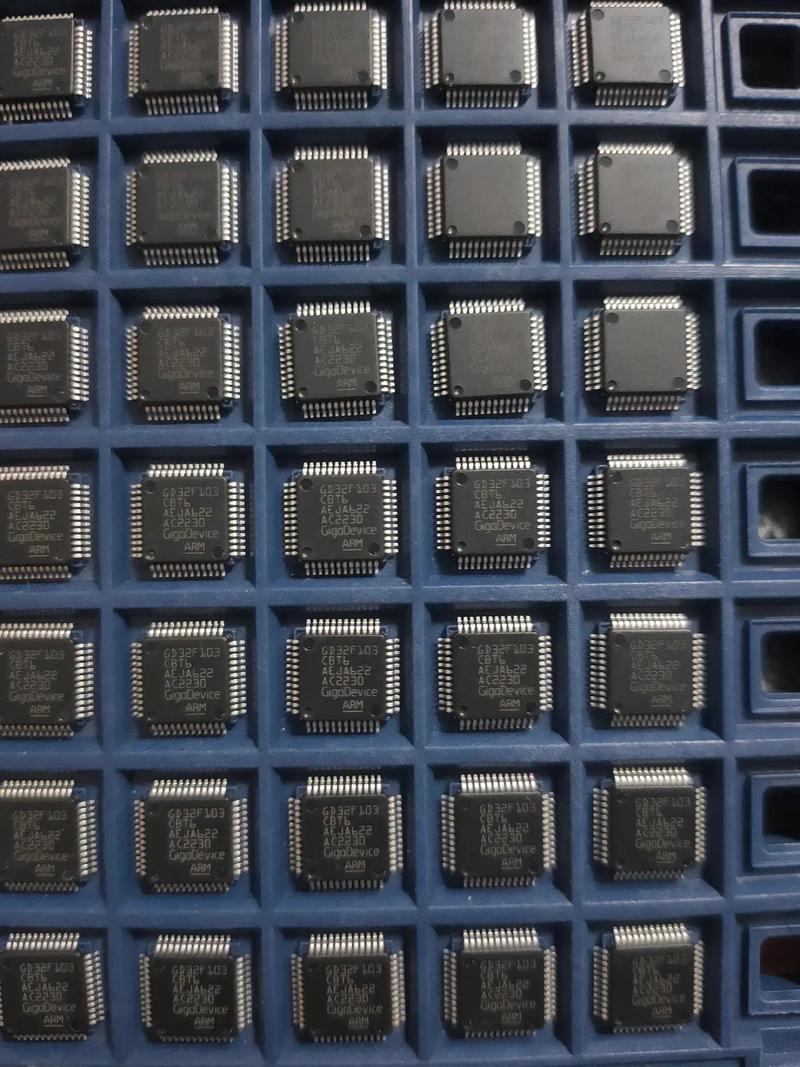
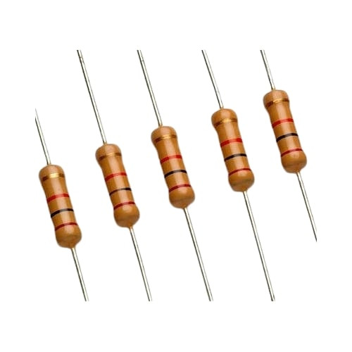
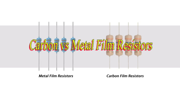
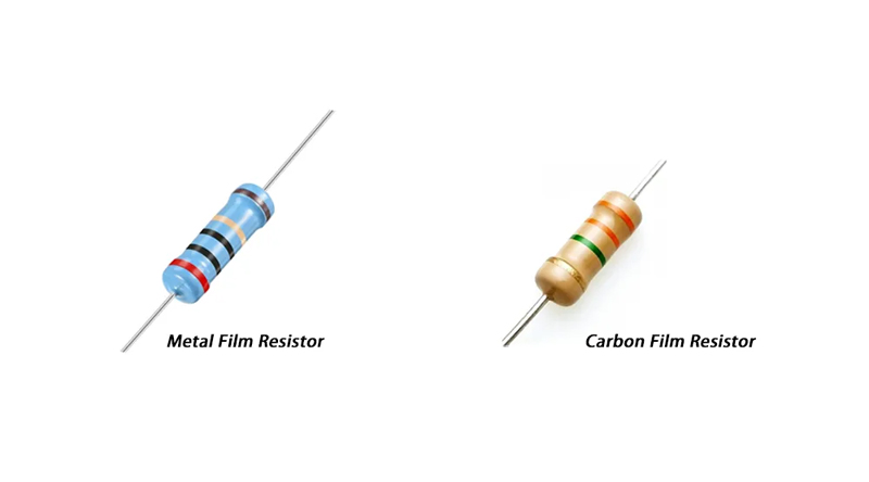
Carbon film resistors are passive two terminal components where a thin layer of carbon is deposited on an insulating ceramic substrate. The resistance value is adjusted by cutting a spiral groove into the carbon layer, which controls the length of the current path.
They are one of the most common general purpose resistors, valued for their simplicity and affordability.
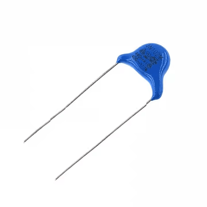
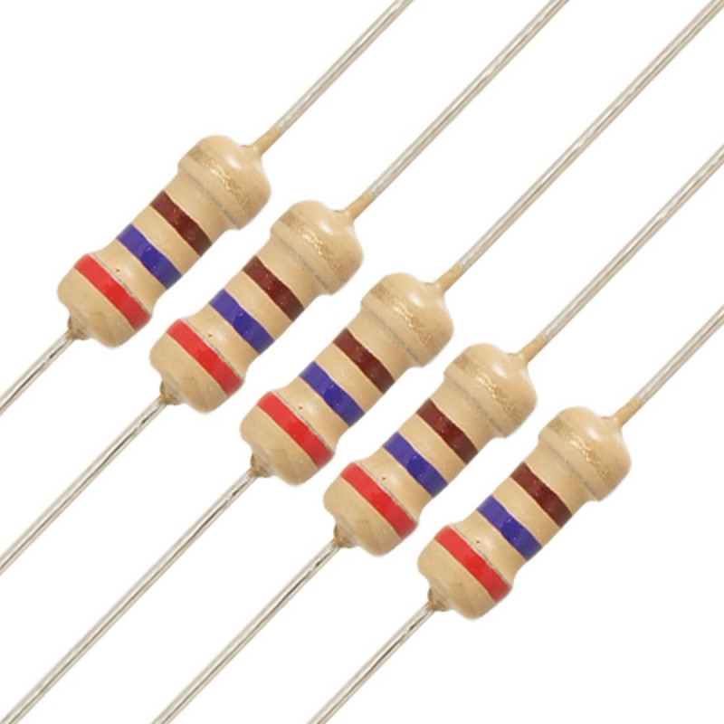
Metal film resistors use a thin layer of metal alloy, typically nickel chromium, deposited on a high purity ceramic substrate. Laser trimming of a helical groove fine tunes the resistance to precise values, making them ideal for applications that demand consistency.
Both types restrict current flow, a fundamental function in nearly every electronic circuit. Choosing the wrong one can lead to drift, noise, or complete failure.
How Do Carbon vs Metal Film Resistors Differ in Manufacturing Process?
Carbon Resistors Manufacturing Process:
- Start with a cylindrical ceramic substrate, usually made of alumina, to provide mechanical support and electrical insulation.
- Deposit a thin carbon film onto the ceramic surface using chemical vapor deposition, where hydrocarbon gases decompose at high temperatures to leave a uniform carbon layer.
- Cut a spiral pattern into the carbon film with a mechanical or laser tool to adjust the resistance value; longer spiral paths create higher resistance.
- Attach metal end caps to the ceramic substrate to connect the carbon film to the lead wires.
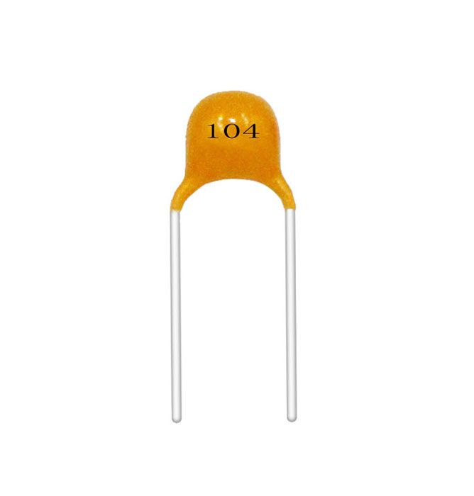
- Apply a protective epoxy coating, often green or khaki, to shield the carbon film from moisture, dust, and physical damage.
- Test resistance values to ensure they fall within the specified tolerance range, typically ±2% to ±5% for standard models.
Metal Film Resistors Manufacturing Process:
- Use a high purity ceramic substrate, often alumina, to minimize thermal drift and ensure stability.
- Deposit a thin metal alloy film, most commonly nickel chromium, onto the substrate using vacuum sputtering or evaporation for uniform thickness.
- Employ laser trimming to cut a precise helical groove into the metal film, allowing for tighter resistance control than carbon film methods.
- Attach tinned copper leads to the metal end caps, which provide reliable electrical contact and improve solderability on PCBs.
- Apply a protective coating, usually blue, to insulate the metal film and protect it from environmental stressors.
- Perform rigorous testing to ensure resistance values meet tight tolerances, often as low as ±0.1% for high precision models.
What Is the Accuracy Difference Between Carbon vs Metal Film Resistors?
Carbon Film Resistors Accuracy:
- Standard tolerance ranges from ±2% to ±5%, with some lower cost models offering only ±10% tolerance.
- Resistance values drift more over time, typically ±5% over 1000 hours of operation, due to the porous nature of the carbon film and sensitivity to moisture.
- Voltage coefficient is higher, meaning resistance changes more significantly with variations in applied voltage, especially at higher voltages.
- Poor consistency across batches; even resistors from the same manufacturer may have slight variations in resistance value.
Metal Film Resistors Accuracy:
- Tight tolerance options range from ±0.1% to ±1%, making them ideal for precision circuits that require consistent performance.
- Minimal long term drift, usually less than ±0.5% over 1000 hours, thanks to the stable metal alloy film and high quality substrate.
- Very low voltage coefficient, so resistance remains stable even with fluctuations in applied voltage, critical for high precision applications.
- Excellent batch consistency, ensuring that every resistor in a production run performs the same way, reducing circuit variations.
Why Do Metal Film Resistors vs Carbon Film Resistors Have Different Temperature Stability?
Temperature stability, measured by the Temperature Coefficient of Resistance (TCR), differs between metal film and carbon film resistors primarily due to their materials and manufacturing processes.
Metal film resistors use nickel chromium alloys, which have a low TCR ranging from ±20 to ±200 ppm/°C. This means their resistance changes very little with temperature fluctuations because the metal alloy maintains a stable structure even when heated or cooled.
The high purity ceramic substrate also helps dissipate heat evenly, reducing localized temperature spikes that cause drift.
Carbon film resistors, on the other hand, have a much higher TCR, typically -200 to -1000 ppm/°C, because carbon’s resistance decreases as temperature rises.
The porous carbon film structure is more susceptible to thermal expansion and contraction, leading to greater resistance drift when exposed to temperature changes. Additionally, the binders used in carbon film resistors break down over time at high temperatures, further reducing stability.
Which Is More Cost-Effective: Carbon Film vs Metal Film Resistors?
Carbon Film Resistors Cost Effectiveness:
- Lower upfront cost; carbon film resistors are 30% to 50% cheaper than metal film resistors of the same power rating and resistance value.
- Simpler manufacturing process reduces production costs, making them ideal for high volume, low cost projects like consumer electronics.
- Wider availability in standard resistance values, reducing lead times and procurement costs.
- No need for expensive laser trimming, further lowering production expenses for manufacturers.
Metal Film Resistors Cost Effectiveness:
- Higher upfront cost due to more complex manufacturing, including vacuum deposition and laser trimming.
- Lower long term costs because of their stability; fewer replacements are needed over the life of the circuit, reducing maintenance and repair expenses.
- Reduced circuit failure rates, which saves money on rework and warranty claims, especially in high precision applications.
- Better value for projects that require tight tolerances; using carbon film resistors in these cases would lead to costly performance issues.
What Are the Noise Level Differences Between Metal Film vs Carbon Film Resistors?
Carbon Film Resistors Noise Levels:
- Higher noise levels, typically 1 to 5 µV/V, due to the granular structure of the carbon film. The uneven distribution of carbon particles causes random fluctuations in current flow, creating thermal and flicker noise.
- Noise increases with applied voltage and temperature, making them problematic in low signal circuits where noise can distort output.
- Flicker noise is more prominent at low frequencies, which can affect audio and analog circuits.
- Noise performance degrades over time as the carbon film ages and absorbs moisture, leading to more inconsistent signal quality.
Metal Film Resistors Noise Levels:
- Very low noise levels, usually less than 0.2 µV/V, because of the uniform metal alloy film structure. The smooth, consistent surface reduces current fluctuations and noise generation.
- Noise remains stable across a wide range of voltages and temperatures, making them ideal for low noise circuits.
- Minimal flicker noise, even at low frequencies, which is critical for audio and precision analog applications.
- Noise performance stays consistent over the resistor’s lifespan, ensuring reliable signal integrity for the life of the circuit.
When Should You Choose Metal Film Resistor vs Carbon Film Resistor for Audio Circuits?
Audio circuits are highly sensitive to noise, tolerance, and stability, as these factors directly impact sound clarity, frequency response, and overall audio quality. The choice between metal film and carbon film resistors in audio applications depends on the project’s fidelity goals, cost constraints, and the specific audio stage being designed.
- Choose metal film resistor when designing high fidelity audio amplifiers. Their low noise levels prevent hiss and distortion, preserving the clarity of the audio signal. This is especially important for preamplifiers and headphone amplifiers where low level signals are amplified.
- Choose metal film resistor for audio equalizers and tone controls. Tight tolerance ensures consistent frequency response across all channels, preventing imbalances in sound quality.
- Choose metal film resistor for digital audio devices like DACs and ADCs. Their stability and low noise ensure accurate conversion between digital and analog signals, reducing jitter and distortion.
- Choose carbon film resistor for budget friendly audio projects where cost is a priority and noise is not a critical concern. Examples include basic portable speakers and low end radios where audio quality is not the primary focus.
- Choose carbon film resistor for power amplifier output stages. These stages handle high currents and voltages, and carbon film resistors’ ability to withstand surge currents makes them a practical choice here, even with slightly higher noise.
How Do Carbon Film vs Metal Film Resistors Perform in High-Pulse Load Scenarios?
Carbon Film Resistors in High-Pulse Loads
- Better pulse handling capability due to carbon’s negative temperature coefficient. As temperature rises during a pulse, resistance decreases, spreading current across the film and reducing localized hot spots that can cause failure.
- Able to withstand higher voltage pulses, up to 15 kV in some models, making them suitable for circuits that experience occasional surge currents like power supplies and welding controls.
- May experience temporary resistance drift after a high pulse, but typically returns to near original value once the circuit cools down.
- More robust in high pulse scenarios than metal film resistors, but still require proper power derating to avoid permanent damage.
Metal Film Resistors in High-Pulse Loads
- Poorer pulse handling compared to carbon film resistors. The metal alloy has a positive temperature coefficient, so resistance increases with heat, leading to localized hot spots that can melt the film or cause permanent damage.
- Limited to lower voltage pulses, usually around 500 V, making them unsuitable for high surge applications.
- Permanent resistance drift or failure is common if exposed to pulses beyond their rating, as the thin metal film is easily damaged by thermal stress.
- Not recommended for circuits with frequent high pulse loads, unless specifically rated for pulse applications.
What Are the Common Applications of Metal Film Resistors vs Carbon Film?
Metal Film Resistors Common Applications
- Precision measurement circuits, including sensors and calibration equipment, where tight tolerance and stability are critical.
- Medical devices like heart rate monitors and blood pressure sensors, where reliable performance can impact patient safety.
- RF and high frequency circuits, as their low parasitic inductance and capacitance reduce signal distortion.
- Feedback and gain setting circuits in amplifiers, where consistent resistance ensures stable gain over time and temperature.
- Test and measurement equipment, including oscilloscopes and multimeters, where accuracy is essential for reliable readings.
Carbon Film Resistors Common Applications
- Power supply input stages, where they handle basic current limiting and voltage division without the need for high precision.
- Consumer electronics like televisions, radios, and toys, where cost is a priority and performance requirements are moderate.
- Buffering and damping networks, which absorb short voltage spikes and reduce ringing in switching circuits.
- Vintage electronic equipment repair, where authenticity and cost effectiveness are key considerations.
- General purpose voltage dividers in circuits where precision is not a primary concern, such as indicator lights and basic control circuits.
What Is the Lifespan Difference Between Carbon Film and Metal Film Resistors?
Carbon Film Resistors Lifespan
- Typical lifespan of 10,000 to 50,000 hours under normal operating conditions (25°C, rated power).
- Lifespan decreases significantly in high temperature or high humidity environments, as moisture and heat break down the carbon film and binders.
- Resistance drift increases over time, with values changing by up to ±5% after 10,000 hours of use, which can lead to circuit performance issues.
- Prone to premature failure if exposed to overvoltage or overcurrent, as the carbon film can burn out or crack.
Metal Film Resistors Lifespan
- Longer lifespan of 50,000 to 100,000 hours under normal operating conditions, thanks to the stable metal alloy and high quality substrate.
- More resistant to high temperature and humidity, maintaining performance even in harsh environments.
- Minimal resistance drift over time, with changes of less than ±0.5% after 50,000 hours, ensuring long term circuit stability.
- More durable and less likely to fail from overvoltage or overcurrent, as the metal film is more resilient than carbon film.
How to Choose Between Resistor Metal Film vs Carbon Film for Your Specific Project?
Below is a comparsion table between carbon vs metal film resistors for your reference:
| Project Requirement | Choose Metal Film Resistor If | Choose Carbon Film Resistor If |
| Tolerance Requirement | ±0.1% to ±1% tolerance is needed for precision circuits | Tolerance of ±2% to ±5% is acceptable for non critical circuits |
| Noise Sensitivity | The circuit handles low level signals (audio, analog, sensors) where noise is a concern | Noise is not critical, such as in power supply or indicator circuits |
| Temperature Stability | The circuit operates in a wide temperature range (25°C to 155°C) or requires minimal drift | The circuit operates in a stable temperature environment (20°C to 60°C) |
| Cost Priority | Long term reliability and performance are more important than upfront cost | Upfront cost is the main concern, and long term drift is acceptable |
| High-Pulse Loads | The circuit has no frequent high pulse loads or uses pulse rated metal film models | The circuit experiences occasional high voltage or current pulses |
| Lifespan Expectation | The project requires a lifespan of 50,000+ hours (industrial, medical devices) | The project has a short to medium lifespan (consumer electronics, toys) |
| Frequency Range | The circuit operates at high frequencies (RF, digital signals) where parasitic effects matter | The circuit operates at low to medium frequencies (DC, basic analog) |
What Mistakes Should You Avoid When Selecting Carbon vs Metal Film Resistors?
Here are mistakes you should aviod when selecting carbon vs metal film resistors:
- Avoid choosing carbon film resistors for precision circuits. Using carbon film resistors in applications that require tight tolerance or low drift will lead to inconsistent performance and circuit failure. Always match the resistor type to the accuracy requirements.
- Avoid ignoring temperature operating ranges. Using metal film resistors in extremely high temperature environments beyond their rating can cause permanent damage, while carbon film resistors will drift significantly in wide temperature swings.
- Avoid overlooking noise requirements. Using carbon film resistors in low noise audio or analog circuits will introduce hiss and distortion, ruining signal quality. Always prioritize metal film resistors for these applications.
- Avoid underestimating pulse loads. Using metal film resistors in circuits with frequent high pulse loads will lead to premature failure. Choose carbon film resistors for these scenarios unless using pulse rated metal film models.
- Avoid choosing based solely on cost. While carbon film resistors are cheaper upfront, they may cost more in the long run due to replacements and rework. Metal film resistors offer better value for precision or long lifespan projects.
- Avoid neglecting lifespan requirements. Using carbon film resistors in projects that need to last 50,000+ hours will result in frequent failures and maintenance. Choose metal film resistors for long term reliability.
- Avoid mismatching power ratings. Both carbon and metal film resistors will fail if operated above their rated power. Always derate resistors by 20% to 50% to ensure reliability, regardless of type.
FAQ About Carbon vs Metal Film Resistors
Q1: Can I replace a carbon film resistor with a metal film resistor in my circuit?
A1: Yes, carbon film resistors can be replaced with metal film resistors as long as the resistance value, power rating, and tolerance match. Metal film resistors offer better stability and lower noise, which can improve circuit performance. Ensure the metal film resistor can handle any pulse loads the circuit may have, as metal film resistors are less robust in high pulse scenarios.
Q2: Are metal film resistors better than carbon film resistors for all applications?
A2: No, metal film resistors are not better for all applications. Carbon film resistors are more cost effective for low precision, high volume projects and perform better in high pulse load scenarios. Metal film resistors are better for precision, low noise, and long lifespan applications, but they come at a higher cost.
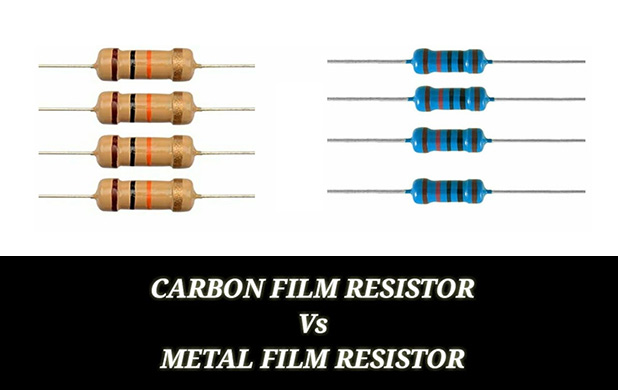
Q3: How can I tell the difference between carbon film and metal film resistors visually?
A3: Visual differences are often clear by color. Carbon film resistors are typically green or khaki, while metal film resistors are often blue. Metal film resistors may also have 5 color bands for tight tolerance, while carbon film resistors usually have 4 color bands. Always check the datasheet for confirmation, as some manufacturers may use different colors.
Q4: Do carbon film resistors have higher power ratings than metal film resistors?
A4: No, both carbon film and metal film resistors are available in similar power ratings, ranging from 0.125W to 10W or higher. Power rating depends on the resistor’s size and construction, not the type. Carbon film resistors can handle higher pulse power, while metal film resistors excel at continuous power dissipation.
Q5: Why do carbon film resistors have a negative temperature coefficient?
A5: Carbon film resistors have a negative temperature coefficient because carbon’s resistance decreases as temperature increases. This stems from carbon’s atomic structure; as temperature rises, more electrons become free to move, increasing conductivity and reducing resistance. This property helps carbon film resistors handle high pulse loads by spreading current evenly.
Q6: Are carbon film resistors still used in modern electronics?
A6: Yes, carbon film resistors are still widely used in modern electronics, especially in cost sensitive consumer devices like toys, radios, and basic power supplies. They are also used in applications that require high pulse handling, such as power supply input stages and welding controls. While metal film resistors are preferred for precision applications, carbon film resistors remain a practical choice for many circuits.
Q7: Do metal film resistors have lower parasitic inductance than carbon film resistors?
A7: Yes, metal film resistors have lower parasitic inductance than carbon film resistors. The laser trimmed helical groove in metal film resistors is more precise and shorter, reducing inductance. This makes metal film resistors better for high frequency circuits, where parasitic inductance can cause signal distortion and phase shifts.