How do electronic manufacturers ensure their products avoid early failures and maintain long-term reliability? The solution lies in a critical testing component known as a burn in board. It is a tool that separates high-quality electronic components from those prone to premature breakdown.
This article breaks down everything about burn in boards, from their core definition to practical applications, design principles, cost factors, and key differences from load boards. Whether working with consumer electronics, industrial equipment, or automotive components, the insights here help make informed decisions about testing processes, material selection, and manufacturer partnerships.
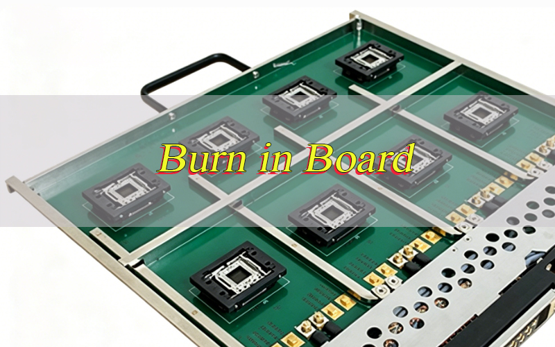
What is a Burn in Board (BIB)?
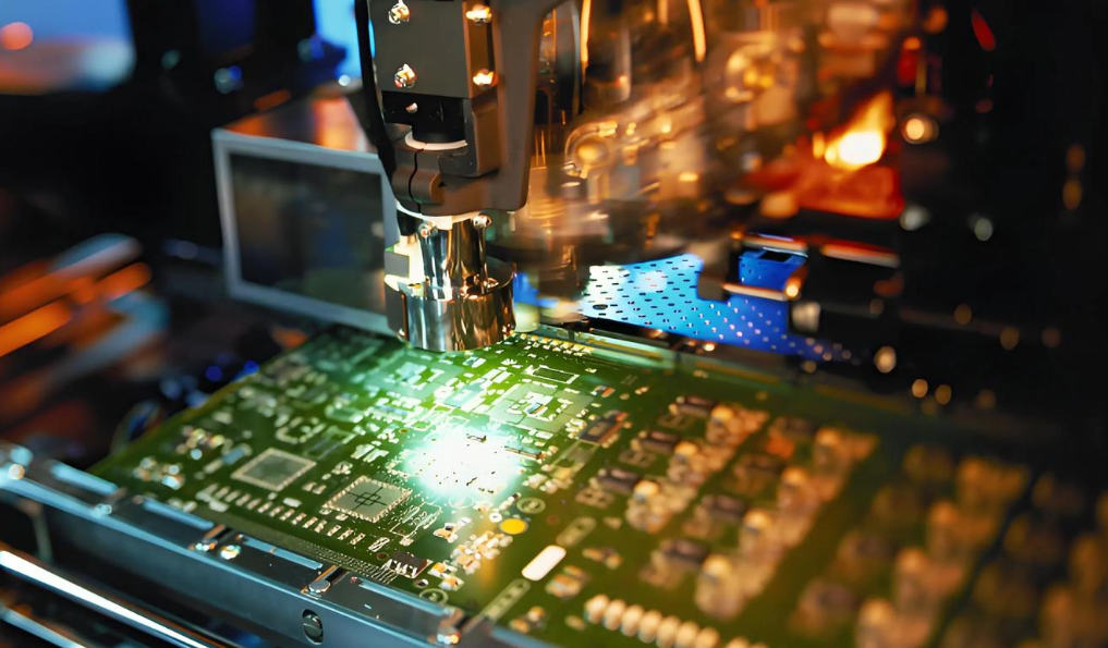
A Burn in Board (BIB), also called an aging board, is a specialized printed circuit board (PCB) built to facilitate burn in testing a reliability screening process for electronic components. Its main function is to expose components to extreme environmental conditions, such as high temperatures, elevated voltage, and continuous operational load, to speed up the detection of potential defects and early-stage failures.
Unlike standard PCBs, burn in boards are engineered to handle harsh testing environments without losing performance. They come with specialized connectors, heat-dissipating structures, and precise wiring to ensure uniform stress application across all tested components. This controlled stress testing simulates years of normal use in just hours or days, letting manufacturers identify and discard faulty components before they reach end users.
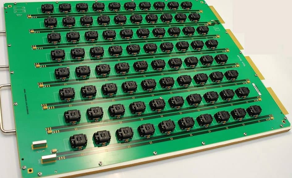
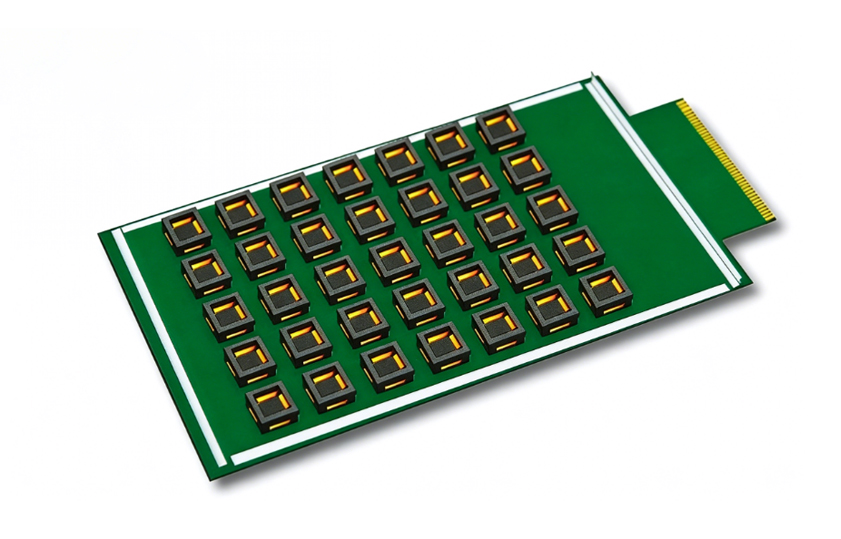
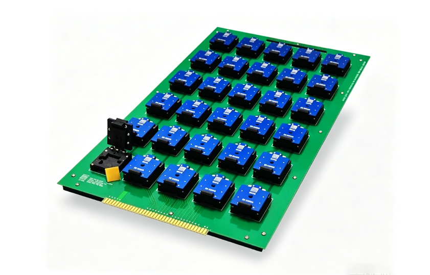
Burn in boards are customized to match the specific form factor and electrical requirements of the components being tested. This customization ensures each component receives the exact stress levels needed to uncover hidden flaws, such as poor solder joints, weak semiconductor bonds, or material inconsistencies that could cause failures after deployment.
Why Do People Use Burn in Boards?
Using burn in boards is a strategic investment in product reliability, addressing common challenges like high return rates, costly recalls, and damaged brand reputation. The following points outline the main reasons manufacturers depend on these specialized boards for electronic component testing.
- Eliminate Early Failures Most electronic component failures happen within the first few hundred hours of use, a phenomenon called infant mortality. Burn in testing with a burn in board accelerates this phase, weeding out defective components before they are integrated into final products. This cuts down on post-purchase failures and the related costs of repairs, replacements, and customer support.
- Ensure Long-Term Reliability Components that pass burn in testing are more likely to maintain performance over their intended lifespan. This is critical for industries like automotive, aerospace, and medical devices, where component failure can lead to safety hazards, regulatory non-compliance, or catastrophic system breakdowns.
- Reduce Warranty and Recall Costs Recalls and warranty claims can drain resources and harm brand trust. By screening components with a burn in board, manufacturers lower the risk of shipping faulty products, reducing warranty expenses and avoiding the negative impact of public recalls.
- Comply with Industry Standards Many industries have strict reliability requirements that require burn in testing. For example, automotive components must meet AEC-Q100 standards, while medical devices need compliance with ISO 13485. Burn in boards enable manufacturers to meet these standards and gain certification for their products.
- Optimize Production Efficiency Identifying defects early in the production process reduces waste and rework. Burn in testing allows manufacturers to address issues at the component level, rather than after assembly, saving time and resources that would otherwise go to disassembling and repairing faulty products.
What is the Difference Between Burn in Board and Load Board?
Burn in boards and load boards are both used in electronic testing, but they serve distinct purposes and operate under different principles. The table below clearly outlines their key differences, helping avoid common confusion between these two critical testing tools.
| Comparison Factor | Burn in Board | Load Board |
| Primary Purpose | Screen for early failures and ensure long-term reliability by subjecting components to extreme stress (high temperature, voltage). | Test the functional performance of components under normal or specified load conditions to verify operational correctness. |
| Testing Environment | Operates in harsh environments, often paired with burn in chambers to maintain high temperatures (70°C+). | Operates in standard laboratory conditions, focusing on normal operating temperatures and voltages. |
| Component Stress Level | Applies elevated stress (above normal operating limits) to accelerate failure detection. | Applies nominal or specified load levels to simulate real-world operational conditions. |
| Design Focus | Built for durability, heat resistance, and uniform stress distribution across components. | Built for precision, signal integrity, and accurate measurement of component performance. |
| Typical Applications | Consumer electronics, automotive components, industrial equipment, medical devices. | Semiconductor testing, PCB functional testing, high-volume production line testing. |
| Testing Duration | Longer duration (hours to days) to ensure thorough stress exposure. | Shorter duration (seconds to minutes) for quick functional verification. |
What Are the Design Principles for a High-Quality Burn in Board?
Designing a high-quality burn in board requires careful consideration of testing requirements, environmental conditions, and component compatibility. The following principles ensure the board delivers consistent, reliable results while withstanding the rigors of burn in testing.
- Thermal Management: Burn in testing generates significant heat, so effective thermal management is essential. The board should feature heat-dissipating structures, such as thick copper traces, thermal vias, or metal substrates, to prevent overheating and ensure uniform temperature distribution across all tested components. This avoids false failures caused by localized hotspots.
- Electrical Compatibility: The board must be electrically compatible with the components being tested, including matching voltage, current, and signal requirements. Proper impedance matching and isolation between circuits prevent cross-talk and ensure accurate stress application.
- Durability and Longevity: Burn in boards are subjected to repeated high-stress testing cycles, so they must be built with durable materials and robust construction. This includes using high-temperature resistant substrates, corrosion-resistant connectors, and reinforced solder joints to withstand extended use.
- Uniform Stress Application: Every component on the board must receive the same level of stress to ensure consistent testing results. This requires precise wiring, balanced load distribution, and careful component placement to avoid variations in voltage or temperature across the board.
- Customization Flexibility: Different components require different testing parameters, so the board should be designed with customization in mind. Modular designs or interchangeable components allow for easy adaptation to different component form factors and testing requirements, reducing the need for multiple dedicated boards.
- Test Monitoring Capability: The board should include provisions for real-time monitoring of component performance during testing. This may include built-in sensors to track temperature, voltage, and current, allowing operators to identify failures as they occur and adjust testing parameters if needed.
Burn in Board Design Guidelines
Following specific design guidelines ensures that burn in boards meet performance standards and deliver reliable testing results. These guidelines address common design pitfalls and provide actionable steps to optimize board performance.
- Select Appropriate Substrate Materials: Choose substrates with high glass transition temperatures (Tg) to withstand high testing temperatures. Common options include FR-4 TG170 or higher, ceramic, or metal-core substrates, depending on the testing environment and component requirements.
- Optimize Trace Width and Spacing: Trace width should be sized to handle the maximum current during testing, preventing overheating and voltage drop. Trace spacing should be sufficient to avoid arcing or cross-talk, especially in high-voltage testing scenarios.
- Use High-Quality Connectors: Select connectors rated for high temperatures and repeated use, such as press-fit or soldered connectors with gold plating to resist corrosion. Ensure connectors provide a secure, low-resistance connection to the tested components.
- Incorporate Thermal Vias: Thermal vias transfer heat from the board surface to internal layers or heat sinks, improving heat dissipation. Place thermal vias near high-heat components and in dense component areas to prevent localized overheating.
- Implement Proper Grounding: A robust grounding system reduces electromagnetic interference and ensures stable electrical performance. Use a solid ground plane and avoid ground loops, which can cause signal noise and inaccurate testing results.
- Design for Easy Component Installation and Removal: The board should allow for quick and secure installation of components, with clear alignment guides and accessible connectors. This reduces testing downtime and minimizes the risk of component damage during handling.
- Include Test Points for Troubleshooting: Add test points at key locations on the board to facilitate troubleshooting and performance verification. Test points allow operators to measure voltage, current, and temperature during testing, helping to identify issues with the board or tested components.
How is Burn in Testing Applied to Electronic Components Using a Burn in Board?
Burn in testing with a burn in board follows a structured process to ensure consistent, effective screening of electronic components. The steps below outline how to apply this testing method, from preparation to post-test analysis.
- Prepare the Burn in Board: Verify that the board is properly configured for the specific components being tested. This includes checking component compatibility, ensuring all connectors are secure, and confirming that thermal management systems are functioning correctly. Calibrate any built-in sensors to ensure accurate temperature and voltage measurements.
- Install Components: Mount the components to be tested onto the burn in board, following proper handling procedures to avoid damage. Ensure components are aligned correctly and securely fastened to prevent poor electrical connections or heat transfer issues.
- Place the Board in a Burn in Chamber: Transfer the loaded burn in board to a burn in chamber, which controls temperature, humidity, and other environmental factors. Set the chamber to the required testing parameters, typically 70°C to 125°C, depending on the component type and industry standards.
- Initiate the Burn in Test: Apply the specified voltage, current, and load to the board, starting the testing cycle. The duration of the test varies based on component type, ranging from 24 to 168 hours. Monitor the test in real time to track component performance and identify any immediate failures.
- Monitor Test Parameters: Continuously check temperature, voltage, and current levels to ensure they remain within the specified range. Any deviations may indicate a problem with the board, chamber, or tested components, requiring immediate adjustment or termination of the test.
- Terminate the Test and Inspect Components: Once the test cycle is complete, remove the burn in board from the chamber and allow it to cool to room temperature. Inspect each component for visible damage, such as bulging capacitors or burnt traces, and perform electrical tests to verify functionality.
- Classify Components: Separate components into passing and failing categories based on test results. Passing components are cleared for further assembly, while failing components are discarded or sent for further analysis to identify the root cause of failure.
What Materials Are Commonly Used to Make Durable Burn in Boards?
The durability and performance of a burn in board depend heavily on the materials used in its construction. The following materials are commonly selected for their ability to withstand high temperatures, electrical stress, and repeated testing cycles.
- FR-4 Glass Epoxy:The most common substrate material for burn in boards, FR-4 glass epoxy offers a good balance of cost, durability, and thermal resistance. FR-4 TG170 or higher grades are preferred for high-temperature testing, as they maintain structural integrity at temperatures up to 170°C. It is widely used for consumer electronics and industrial components testing.
- Ceramic Substrates: Ceramic substrates, such as alumina (Al2O3) and aluminum nitride (AlN), provide excellent thermal conductivity and high-temperature resistance. They are ideal for testing high-power components, such as automotive semiconductors and industrial power modules, where heat dissipation is critical.
- Metal-Core PCBs: Metal-core PCBs (MCPCBs) feature a metal base, typically aluminum or copper, which enhances heat dissipation. They are commonly used for burn in boards testing LED components, power amplifiers, and other high-heat devices. The metal core acts as a heat sink, reducing component temperature during testing.
- High-Temperature Copper Foil: Thick copper foil (2 oz or higher) is used for traces and ground planes to improve current-carrying capacity and heat dissipation. Gold-plated copper foil is often used for connectors and test points to resist corrosion and ensure low-resistance connections.
- Heat-Resistant Solder: Solder with a high melting point, such as lead-free solder (Sn-Ag-Cu) or high-temperature leaded solder (Sn-Pb), is used to assemble burn in boards. This prevents solder joints from melting during high-temperature testing, ensuring reliable electrical connections.
- High-Temperature Connectors: Connectors made from heat-resistant materials, such as PEEK or LCP, are used to connect the burn in board to testing equipment. Gold-plated contacts provide corrosion resistance and ensure stable electrical performance over repeated testing cycles.
How Much Does a Burn in Board Cost?
The cost of a burn in board varies based on several factors, including design complexity, materials, customization requirements, and order quantity. Understanding these factors helps manufacturers budget effectively and select the most cost-efficient solution for their testing needs.
- Design Complexity: Simple burn in boards for basic components (e.g., resistors, capacitors) cost less, typically ranging from $100 to $500 per unit. Complex boards for high-power or specialized components (e.g., automotive semiconductors, medical devices) require more intricate design and materials, costing $500 to $2,000 or more per unit.
- Substrate Material: FR-4 boards are the most cost-effective option, while ceramic and metal-core substrates increase costs by 30% to 100%. The choice of material depends on the testing environment and component requirements, with high-temperature applications requiring more expensive materials.
- Customization: Customized boards, tailored to specific component form factors or testing parameters, cost more than standard designs. Customization costs include engineering time, tooling, and prototype development, which can add $200 to $1,000 per board.
- Order Quantity: Bulk orders reduce per-unit costs significantly. Ordering 10 or more boards can lower per-unit costs by 20% to 40% compared to single-unit orders. Manufacturers often offer volume discounts for large orders, making it more cost-effective to stock boards for ongoing testing needs.
- Additional Features: Boards with built-in sensors, modular components, or advanced thermal management systems cost more. For example, a board with temperature sensors and real-time monitoring capabilities may cost 50% more than a basic board without these features.
- Manufacturing Tolerances: Tighter manufacturing tolerances, required for high-precision testing, increase costs. For example, boards with precise trace spacing or impedance control may cost 25% to 50% more than standard-tolerance boards.
What Should You Look for When Choosing a Reliable Burn in Board Manufacturer?
Selecting a reliable burn in board manufacturer is critical to ensuring consistent testing results, on-time delivery, and long-term product reliability. The following factors help identify manufacturers that can meet your specific needs and deliver high-quality boards.
- Industry Experience: Look for manufacturers with a proven track record in producing burn in boards for your industry. Experience with automotive, medical, or industrial components ensures the manufacturer understands the unique testing requirements and standards for your application.
- Quality Control Processes: Reliable manufacturers implement strict quality control processes, including incoming material inspection, in-process testing, and final validation. Ask about their quality management system, such as ISO 9001 certification, and request documentation of test results for their boards.
- Customization Capabilities: Choose a manufacturer that can customize boards to your specific component and testing requirements. This includes the ability to design boards for unique form factors, adjust thermal management systems, and integrate specialized features like sensors or monitoring tools.
- Material Sourcing: Ensure the manufacturer uses high-quality, industry-approved materials for board construction. Ask about their material suppliers and verify that they use genuine, certified materials to avoid performance issues or premature board failure.
- Delivery Timeframes: On-time delivery is critical to maintaining production schedules. Look for manufacturers with a reputation for meeting delivery deadlines, even for custom orders. Ask about their lead times and contingency plans for unexpected delays.
- Technical Support: A reliable manufacturer provides ongoing technical support, including assistance with board design, testing optimization, and troubleshooting. This ensures you can resolve any issues quickly and maximize the performance of your burn in boards.
- Pricing Transparency: Choose a manufacturer that provides clear, detailed pricing with no hidden fees. Ask for a breakdown of costs, including design, materials, manufacturing, and shipping, to ensure you can budget effectively and avoid unexpected expenses.
What is the Correct HS Code for Burn in Boards for Import and Export?
The primary HS code for burn in boards is 8534.00.90. This code covers printed circuit boards (PCBs) that are not specifically classified under other subheadings, including specialized boards used for testing, such as burn in boards. This code applies to both single-layer and multi-layer burn in boards, regardless of their design complexity or customization.
It is important to note that HS codes may vary slightly by country or region, so it is recommended to verify the code with local customs authorities before importing or exporting. Some countries may classify burn in boards under subheadings of 8534.00, depending on factors like material composition (e.g., ceramic vs. FR-4) or intended use.
When completing customs documentation, provide a detailed description of the burn in board, including its purpose (reliability testing of electronic components), material composition, and design features. This ensures customs officials can verify the correct classification and avoid delays or penalties.
FAQs About Burn in Board
Q1: Can burn in boards be reused for different component types?
A1: Yes, many burn in boards are designed with modular components or interchangeable connectors, allowing them to be reused for different component types. Modular designs reduce the need for multiple dedicated boards, saving costs and storage space. However, reuse requires reconfiguration to match the new component’s electrical and physical requirements, including adjusting trace spacing, voltage settings, and component mounting points.
Q2: How long does a typical burn in test with a burn in board take?
A2: The duration of a burn in test varies based on component type and industry standards. Most tests last between 24 and 168 hours. Consumer electronics components often require 24 to 48 hours of testing, while automotive and medical components may need 72 to 168 hours to ensure long-term reliability. The goal is to apply enough stress to reveal early failures without damaging functional components.
Q3: Do all electronic components require burn in testing with a burn in board?
A3: No, not all components require burn in testing. Low-cost, low-reliability components (e.g., basic resistors for toys) may not need testing, as the cost of testing outweighs the risk of failure. However, components used in critical applications (automotive, medical, aerospace) or high-value products (servers, industrial equipment) almost always require burn in testing to ensure reliability and compliance with industry standards.