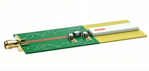
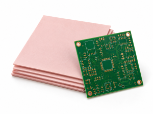
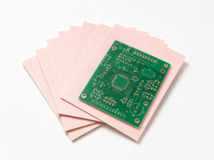
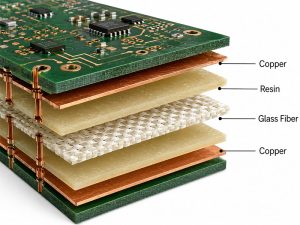
An amplifier circuit PCBâ is a specialized printed circuit board designed to support and interconnect components that increase signal amplitude while maintaining fidelity. This article explores its types, design strategies, high-power builds, component selection, common issues, and selection criteria to help you optimize layout and performance.
Designing reliable amplifier circuits often comes with challenges that can derail projects.
Poor signal integrity due to mismatched trace impedance
To address these pain points, EBest Circuit (Best Technology) offers professional amplifier PCBâ manufacturing and assembly services tailored for optimal performance and manufacturability.
Impedance-controlled routing and PCB traces artâ for signal clarity
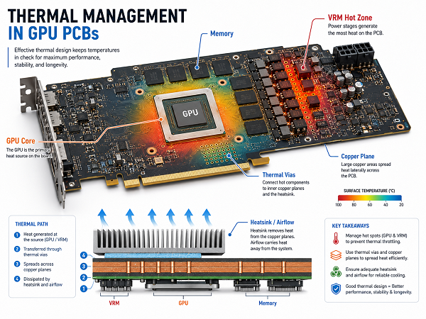
Integrated thermal vias and copper pours for heat dissipation
Star grounding and shielding techniques to suppress EMI
DFM-optimized layouts ensuring smooth mass production
Fast-turn prototyping and volume production with transparent pricing
EBest Circuit (Best Technology) is a leading PCBA manufacturer specializing in high-performance amplifier circuit PCBâ solutions. With advanced fabrication capabilities and strict quality control, we deliver reliable boards for audio, RF, and industrial applications. Pls feel free to contact us at sales@bestpcbs.com for expert support.
What Is an Amplifier Circuit PCB?
An amplifier circuit PCBâ is the engineered foundation that mechanically supports and electrically connects all components required to increase the amplitude of a signalâwhether audio, radio frequency (RF), or power. Beyond simple connectivity, it manages critical factors like power delivery, signal integrity, and heat dissipation to ensure stable, high-fidelity performance.
Depending on the application, different base materials and technologies are selected to meet specific electrical and thermal demands. The most common types used in amplifier PCBâ manufacturing include:
FR-4 (Standard): The most widely used substrate for general-purpose amplifier circuit boards, offering a balance of cost, mechanical strength, and electrical insulation. Ideal for consumer audio and mid-power designs.
High-Tg FR-4: Modified for higher glass transition temperatures, providing better thermal stability and reliability for power amplifier circuit PCB layoutâ in demanding environments.
HDI (High-Density Interconnect): Utilizes microvias and fine lines to accommodate complex PCB amplifier circuitâ designs with high component density, often used in compact Class D amplifiers.
Metal Core PCB (MCPCB): Features an aluminum or copper base for superior thermal conductivity, essential for 3kw power amplifier driver circuit PCB layoutâ where heat management is critical.
RF/Microwave Laminates (e.g., Rogers): Low-loss materials designed for high-frequency applications, crucial for class d amplifier circuit PCB layoutâ and wireless communication amplifiers to maintain signal purity.
By selecting the right board type and layout strategy, designers can effectively manage the trade-offs between performance, size, and cost in any amplifier circuit PCBâ project.
What Are the Key Types of Amplifier PCB Circuits?
Amplifier PCBs vary by application and topology:
Type
Typical Use
Key Feature
Audio Amplifier PCB
Home/car audio
Low distortion, high fidelity
RF Amplifier PCB
Wireless comms
High-frequency stability
Class D Amplifier PCB
Efficient power amps
PWM switching, compact size
Instrumentation Amp PCB
Sensors/measurement
High CMRR, precision
Power Amplifier PCB
1000Wâ3KW systems
Robust thermal handling
How to Design a High-Performance Amplifier PCB Layout?
Optimizing an amplifier circuit PCB layoutâ requires attention to signal paths, grounding, and thermal design.
Keep input and output traces short and separated to avoid feedback
Use ground planes and star grounding to minimize noise
Place decoupling capacitors close to power pins
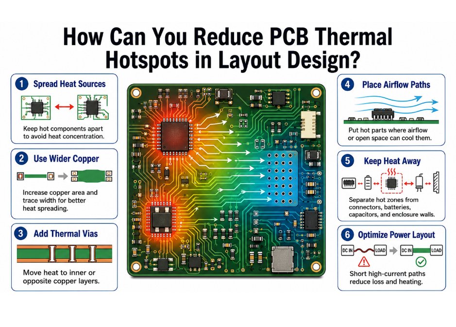
Implement thermal vias under high-power devices
Follow power amplifier circuit PCB layoutâ best practices for EMI reduction
For complex designs like a 1000w amplifier circuit diagram PCB, simulation tools help validate signal integrity before fabrication.
How to Build a 1000W or 3KW Power Amplifier PCB?
High-power builds demand careful planning:
Select MOSFETs or IGBTs rated for voltage/current
Use thick copper (2ozâ4oz) for current-carrying traces
Design 3kw power amplifier driver circuit PCB layoutâ with adequate heatsinking
Ensure proper isolation between high-voltage and low-voltage sections
Validate with thermal imaging and load testing
What Components Are Used in an Amplifier Circuit PCB?
Core components include:
Amplification devices: BJTs, MOSFETs, op-amps, Class D ICs
Passive elements: Resistors, capacitors, inductors for filtering
A typical PCB amplifier circuitâ integrates these for stable gain and protection.
Common Problems in Amplifier PCB Layout and How to Fix Them
Problem
Cause
Solution
Oscillation
Poor grounding, long feedback loops
Shorten traces, improve grounding
Overheating
Inadequate copper, no thermal vias
Add vias, increase copper area
Noise/hum
Ground loops, unshielded traces
Star ground, shield sensitive lines
Distortion
Incorrect biasing, poor layout
Verify bias points, optimize routing
Failure to start
Power sequencing issues
Add soft-start or delay circuits
How to Choose the Right Amplifier PCB for Your Application?
Consider:
Required power output (e.g., 1000W vs 3KW)
Frequency range and signal type
Environmental conditions (temperature, vibration)
Size and form factor constraints
Budget and production volume
Matching specs to needs ensures optimal performance from your amplifier circuit board.
Overall, an amplifier circuit PCBâ is essential for delivering clean, amplified signals across audio, RF, and power applications. This guide covered definitions, types, layout optimization, high-power design, components, troubleshooting, and selection criteria to help you build better boards. For expert manufacturing and assembly of amplifier PCBâ solutions, pls feel free to contact us anytime at sales@bestpcbs.com.
FAQs About Amplifier Circuit PCB
Q: Can I use a standard PCB for a power amplifier?â
A: Not recommendedâhigh-current designs need thicker copper and thermal management.
Q: Whatâs the difference between Class AB and Class D layouts?â
A: Class D uses switching topology requiring careful EMI control; Class AB is linear but less efficient.
Q: How do I reduce noise in my amplifier PCB?â
A: Use proper grounding, shielding, and keep analog/digital sections isolated.
Q: Do you provide power amplifier circuit diagram with PCB layoutâ services?â
A: Yes, EBest Circuit offers full design-to-production support.
If youâre designing a PCB, you may wonder: which is better for your project, a 0 ohm resistor, a jumper, or a wire? This guide breaks down everything you need to know about 0 ohm resistors, their specs, functions, and how they compare to jumpers and wires. Youâll learn how to choose, test, and use 0 ohm resistors effectively so you can make the right choice for your PCB. Keep reading to solve all your doubts.
What Is A 0 Ohm Resistor?
A 0 ohm resistor (or zero ohm resistor) is a passive electronic component that acts as a jumper or conductor in a standard resistor package. It is essentially a wire link packaged like a regular resistor, designed to connect traces on a printed circuit board without the need for separate jumpers or wires.
Contrary to its name, it does not have true 0 ohm resistance. Instead, it has a very low resistance, typically between 0.01 ohms and 0.1 ohms, depending on the manufacturer and package size. This low resistance lets it conduct current almost as efficiently as a wire, while retaining the form factor of a resistor, making it compatible with standard PCB assembly processes.
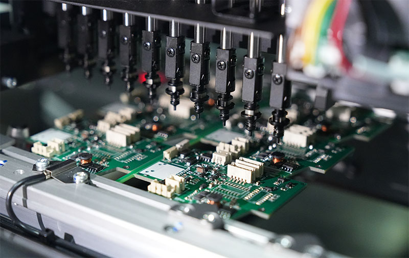
0 ohm resistors come in standard packages like 0402, 0603, 0805, and 1206. They integrate easily into PCB layouts using automated pick-and-place machines and are widely used in PCB design to simplify routing, enable design flexibility, and facilitate testing or modification.
What Is The Resistance Of A 0 Ohm Resistor?
A 0 ohm resistor does not have exactly 0 ohms of resistance. While it is often referred to as a zero ohm resistor, true zero resistance is not physically possible, and these components have a very low actual resistance instead.
Its actual resistance, called typical or nominal resistance, ranges from 0.01 ohms to 0.1 ohms, with most manufacturers specifying a maximum resistance of 0.1 ohms. This small resistance originates from the material used, usually a thin metal film or carbon film, and the physical size of the resistor itself.
For practical PCB use, this resistance is negligible and does not significantly affect current flow or voltage drops.Always check the datasheet for the exact resistance value, as it varies slightly by brand and package type.
What Does A 0 Ohm Resistor Do?
A 0 ohm resistor serves three main functions in PCB design, all simplifying circuit design and assembly.
First, it acts as a jumper or conductor. It connects two PCB points without needing a separate wire or jumper.
Second, it provides design flexibility. If youâre unsure about a connection for testing, different configurations, or future modifications, insert a zero ohm resistor temporarily. You can remove it later if needed.
Third, it facilitates automated assembly. Since 0 ohm resistors use standard resistor packages, they work with the same pick-and-place machines as other resistors. This eliminates manual jumper installation.
Additionally, 0 ohm resistors can break ground loops, isolate circuits, or mark test points on a PCB.
Why 0 Ohm Resistor Is Used In PCB?
0 ohm resistors are a staple in PCB design for practical reasons jumpers and wires cannot match.
They simplify PCB routing. When two components need connection but their pads are not adjacent, a 0 ohm resistor bridges the gap. No complex wire routing or vias are needed.
They support automated manufacturing. Manual jumpers take time to install and are prone to errors. 0 ohm resistors fit seamlessly into automated pick-and-place and soldering processes.
They enable design flexibility. Engineers use 0 ohm resistors to create modular PCBs. Different sections can be connected or disconnected by adding or removing the resistor.
They improve PCB reliability. 0 ohm resistors are less likely to come loose than jumpers. Their standard package protects the connection from damage during handling or operation.
What Is The Color Code For A 0 Ohm Resistor?
0 ohm resistors have a simple color code, easy to identify even for beginners, and it differs significantly from standard resistors that use multiple color bands to indicate resistance values. Axial-lead through-hole 0 ohm resistors, in particular, are generally marked with a single black band. This black band serves as the symbol for 0 ohms in resistor color coding, as black is universally used to represent the digit 0 in resistor color marking systems.
While the single black band is the most common marking for 0 ohm resistors, some may have two black bands, though this is less prevalent. For four-band 0 ohm resistors, the first three bands are black to signify 0 ohms. The fourth band is used for indicating tolerance and can be gold, silver, or omitted entirely, depending on the manufacturerâs specifications. Gold typically indicates a ±5% tolerance and silver a ±10% tolerance, consistent with standard resistor color code conventions.
This simplified color code design makes it easy to distinguish 0 ohm resistors from other components on a PCB, which is critical for efficient assembly and troubleshooting. It is worth noting that surface-mount 0 ohm resistors are often marked with one or multiple â0â instead of color bands. The color code, however, remains the standard for through-hole types, ensuring consistency in identification across different resistor formats.
How Much Current Can A 0 Ohm Resistor Handle?
A 0 ohm resistorâs current-carrying capacity is not fixed and depends on three key factors: its package size, the material it is made of, and the ambient temperature of the operating environment. These factors work together to determine how much current the resistor can safely conduct without experiencing failure.
Package size is a primary determinant of current capacity, with smaller packages handling less current and larger packages accommodating more. For instance, a 0402 0 ohm resistor typically handles 0.5A to 1A, a 0603 package handles 1A to 2A, and a 1206 package can handle 2A to 3A. It is important to check the 0 ohm resistor datasheet for the exact current rating, as values can vary slightly by manufacturer.
Exceeding the specified current rating can lead to serious issues, including the resistor overheating, melting, or failing entirely, which can damage the entire PCB. For high-current circuits, it is crucial to choose a zero ohm resistor with a current rating that exceeds the circuitâs maximum current to ensure safe and reliable operation.
0 Ohm Resistor Datasheet Specification
A 0 ohm resistorâs datasheet has critical specifications every PCB engineer should review before selection. Below is a detailed table of key datasheet specifications for easy reference:
Specification Type
Typical Value/Description
Notes
Typical Resistance
0.01 ohms â 0.1 ohms
Actual resistance varies slightly by manufacturer and package size
Maximum Resistance
0.1 ohms (most manufacturers)
Critical for ensuring minimal voltage drop in circuits
Current Rating
0.5A â 3A (varies by package size)
0402: 0.5A-1A; 0603:1A-2A; 1206:2A-3A; check datasheet for exact values
Voltage Rating
25V â 100V
Depends on resistor material and package design
Operating Temperature Range
-55°C to 155°C
Temperature above 70°C may require current derating
Package Size
0402, 0603, 0805, 1206 (common)
Larger packages have higher current-carrying capacity
Material
Metal film, carbon film, or thick film
Affects resistance consistency and temperature stability
Essential for proper installation and long-term performance
Always refer to the datasheet to ensure compatibility with your PCBâs operating conditions. Ignoring specs can lead to component failure and PCB malfunctions.
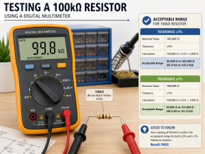
How To Test 0 Ohm Resistor?
Testing a zero ohm resistor is straightforward with a multimeter, and the process differs slightly for on-PCB and off-PCB testing. Below are the detailed, step-by-step test steps, along with result judgment and key notes:
Prepare tools and confirm safety: Use a digital multimeter (ensure it is calibrated to avoid inaccurate readings). If testing on a PCB, turn off the circuit power and disconnect the power source to prevent short circuits or false readings caused by residual voltage.
Perform the test operation: For off-PCB testing, touch the two probes of the multimeter firmly to the two leads of the 0 ohm resistor. For on-PCB testing, touch the probes to the two pads of the resistor on the PCB, avoiding contact with adjacent components to prevent interference.
Judge test results: A normal 0 ohm resistor will show a reading between 0.01 ohms and 0.1 ohms, which aligns with its nominal low resistance. A reading higher than 10 ohms indicates the resistor is faulty or damaged. A reading of âOLâ (open loop) means the resistor is open and cannot conduct current, requiring replacement.
Post-test notes: After testing, turn off the multimeter and restore the circuit connection (if on-PCB testing). Regular testing of 0 ohm resistors in key circuits helps detect potential failures early and avoid damage to the entire PCB.
Difference Between 0 Ohm Resistor VS Jumper: Which Is Better?
Choosing between a zero ohm resistor and a jumper depends on your PCBâs design, manufacturing process, and requirements. Below is a detailed comparison table to help you decide:
Feature
0 Ohm Resistor
Jumper
Form Factor
Standard resistor package (0402, 0603, etc.), fits PCB pads
Small wire loop or pin header, requires dedicated jumper pads
Automated Assembly
Compatible with pick-and-place machines, no manual labor needed
Requires manual installation, slow and prone to errors
Design Flexibility
Easily removable/replaceable for circuit modifications or testing
Permanent once installed; difficult to remove without damaging the PCB
Current Capacity
Limited by package size (0.5Aâ3A)
Higher current capacity (depends on wire gauge)
Reliability
High; soldered securely to PCB, less likely to come loose
Low; prone to loosening or breaking due to vibration or handling
Low-volume projects, manual assembly, high-current applications where space is not an issue
Difference Between 0 Ohm Resistor VS Wire: Which Is Better?
A zero ohm resistor and a wire both conduct current, but they differ in form factor, usability, and reliability. Below is a detailed comparison table to help you choose the right option for your PCB:
Feature
0 Ohm Resistor
Wire
Form Factor
Compact, standard resistor package; fits neatly on PCB pads
Flexible or rigid wire; requires space for routing, may cause clutter
Automated Assembly
Fully compatible with pick-and-place and soldering machines
Requires manual routing and soldering; not suitable for automated lines
PCB Routing
Simplifies routing; bridges gaps between non-adjacent pads without vias
Requires complex routing; may block other components or create short circuits
Modification
Easily removed or replaced for circuit changes or testing
Difficult to modify; cutting or re-soldering may damage the PCB
Resistance
Low (0.01â0.1 ohms); consistent across temperature changes
Very low (depends on length and gauge); increases with length
Best For
Compact PCBs, automated manufacturing, modular designs, test points
High-current applications, large PCBs, temporary connections during prototyping
How To Choose The Right 0 Ohm Resistor for Your PCB Project?
Choosing the right 0 ohm resistor requires considering five core, evidence-based factors to ensure compatibility, reliability, and optimal performance for your PCB project. Below are the detailed, concise guidelines:
Select the appropriate package size: Choose based on your PCBâs space constraints and current requirements. Compact PCBs are ideal for 0402 packages, while 0603 and 0805 suit general-purpose designs. For high-current scenarios, 1206 packages are preferred as they offer higher current-carrying capacity. Ensure the package fits existing PCB pads to avoid assembly issues.
Verify the current rating: The current rating must exceed the maximum current of your circuit to prevent overheating, melting, or resistor failure. Typical ratings vary by package: 0402 (0.5Aâ1A), 0603 (1Aâ2A), 1206 (2Aâ3A). Always check the manufacturerâs datasheet for exact values, as material and ambient temperature also affect current capacity.
Confirm the resistance value: Aim for a nominal resistance of 0.01â0.1 ohms, the standard range for 0 ohm resistors. This low resistance ensures negligible voltage drop and does not interfere with circuit performance. Exact values vary slightly by brand and package, so cross-check the datasheet to avoid selecting components with excessive resistance.
Match to your application scenario: Align the resistor with your PCBâs manufacturing and functional needs. Use 0 ohm resistors for automated assembly, modular designs, or temporary connections for testing. Opt for jumpers or wires instead for low-volume manual assembly or high-current applications where space is not limited.
Choose a reputable manufacturer and review the datasheet: Select reliable manufacturers to ensure consistent performance and quality, as low-quality 0 ohm resistors may have unstable resistance or poor durability. Always review the datasheet to confirm key specs (voltage rating, operating temperature, material) and ensure compatibility with your PCBâs operating environment.
FAQs About Zero Ohm Resistor
Q1: Is there voltage across a 0 ohm resistor?
A1: No, there is no significant voltage across a 0 ohm resistor. 0 ohm resistors have very low resistance, so the voltage drop is negligible. For example, 1A through a 0.1 ohm 0 ohm resistor creates a 0.1V drop, too small to affect most circuits.
Q2: Can you jump a 0 ohm resistor?
A2: Yes, you can jump a 0 ohm resistor, but it is unnecessary. A 0 ohm resistor already acts as a jumper. If it is faulty, you can temporarily jump it with a wire to test the circuit before replacement.
Q3: Can a wire be considered a 0 ohm resistor?
A3: No, a wire cannot be considered a 0 ohm resistor. Wires lack the standard resistor package and specs. 0 ohm resistors are designed for PCB assembly and modularity, while wires are not.
Q4: Can you replace a zero-ohm resistor with a wire?
A4: Yes, you can replace a zero-ohm resistor with a wire in most cases. Both conduct current with low resistance, so the circuit works the same. This removes modification flexibility and compatibility with automated assembly.
Q5: Is a 0 ohm resistor a short?
A5: No, a 0 ohm resistor is not a short circuit. A short has zero resistance, while a 0 ohm resistor has 0.01â0.1 ohms. This small resistance prevents infinite current flow, making it safe for circuits.
Q6: Is 0 ohms good continuity?
A6: Yes, 0 ohms or very low resistance indicates good continuity. Continuity tests check for complete circuits. A 0 ohm reading means the path is unobstructed and current flows freely.
Q7: Is 0 ohms open or closed?
A7: 0 ohms indicates a closed circuit. A closed circuit allows current flow. An open circuit shows âOLâ on a multimeter, meaning no current can flow.
Q8: Is a 0 ohm resistor a fuse?
A8: No, a 0 ohm resistor is not a fuse. Fuses break to protect circuits from overcurrent. 0 ohm resistors conduct current and fail when overloaded but do not act as protective fuses.
What makes automotive grade MCPCB the most reliable solution for high heat high vibration vehicle electronics, and why should you choose EBest as your long term manufacturing partner? This guide covers core performance, certifications, design rules, real world applications, common pain points, and ordering support for automotive grade MCPCB all backed by EBestâs 20+ years of one stop PCB experience, strict quality systems, and fast delivery to keep your automotive projects on track.
Why Choose EBest as Your Top Source for Automotive Grade MCPCB?
When you sourceautomotive grade MCPCB, you need consistent quality, on time delivery, full supply chain stability, and responsive technical support. EBest delivers automotive grade MCPCB with industry leading thermal conductivity, full automotive qualification, stable mass production yield, and expedited prototyping to meet tight project timelines.
Key specifications include wide operating temperature range, high thermal conductivity dielectric, reinforced mechanical structure, and full compliance with automotive standards.
We provide full life cycle support from prototype design to mass production, with stable material supply and professional technical team to ensure your project runs smoothly. Trust EBest for your next automotive grade MCPCB order and experience reliable performance from prototype to mass production.
What Certifications Back EBest Automotive Grade MCPCB Quality?
EBest holds complete authoritative certifications to ensure every automotive grade MCPCB meets global automotive safety and quality standards. Each certification brings real value to your project and reduces compliance risks.
IATF 16949: Full process control, fully traceable production, eliminates hidden quality risks for automotive series production.
ISO 9001:2015: Stable quality management system ensures consistent performance in every batch.
ISO 13485:2016: High reliability control standard suitable for safety critical automotive electronics.
AS9100D: Aerospace level stability to withstand extreme temperature, vibration, and harsh environments.
REACH: Full environmental compliance meeting EU market requirements.
RoHS: Restriction of hazardous substances, safe for automotive assembly and usage.
UL: Safety certification for high power and high voltage automotive circuits.
What Are the Biggest Challenges with Automotive Grade MCPCB and How to Fix Them?
In actual automotive research and development and mass production, automotive grade MCPCBoften faces multiple pain points that affect performance, yield and delivery. EBest provides targeted solutions for each core challenge to ensure stable application in harsh vehicle environments.
Pain Point 1: Insufficient heat dissipation leads to component overheating and early failure. EBest’s Solution: Use high thermal conductivity dielectric layers and optimized thermal paths to rapidly dissipate heat and maintain stable component temperatures.
Pain Point 2: Solder joint cracking or board delamination under high vibration and thermal cycling. EBest’s Solution: Adopt automotive grade base materials and reinforced structural design to enhance mechanical strength and reliability.
Pain Point 3: Low production yield caused by poor design for manufacturing (DFM). EBest’s Solution: Provide free DFM review and design optimization before production to improve manufacturability and batch consistency.
Pain Point 4: Inconsistent quality and lack of traceability in mass production. EBest’s Solution: Implement IATF 16949 process control and full material traceability to ensure stable quality in every batch.
Pain Point 5: Long lead times that delay automotive project development and launch. EBest’s Solution: Offer rapid prototyping and expedited production lines, with urgent orders shipped within 24 hours.
Pain Point 6: Failure to meet automotive industry certifications and customer audit requirements. EBest’s Solution: Maintain full certifications including IATF 16949, UL, RoHS, and REACH for direct compliance with automotive standards.
Pain Point 7: Unstable performance in extreme high low temperature under hood environments. EBest’s Solution: Use wide temperature range materials and strict reliability testing to ensure stable operation from -40°C to +150°C.
What Is Automotive Grade MCPCB and How Does It Work?
Automotive grade MCPCB is a metal core printed circuit board built specifically for harsh vehicle environments. It uses a three layer structure copper circuit, high thermal dielectric, and metal base plate. This structure quickly pulls heat from power components to lower operating temperatures and extend service life. Unlike standard PCBs, automotive grade MCPCB withstands extreme temperatures, vibration, and thermal cycling without failure, making it the preferred core component for high power and high reliability automotive electronics.
How Does Automotive Grade MCPCB Improve Thermal Performance?
Thermal performance is the core advantage of automotive grade MCPCB, directly addressing the high heat demands of automotive systems. By optimizing material selection and structural design, it achieves efficient heat transfer and stable operation in extreme environments.
Uses high thermal conductivity dielectric layers to speed up heat transfer
Metal base (aluminum/copper) provides large area heat dissipation
Optimized thermal via design enhances vertical heat conduction
Low thermal resistance reduces component junction temperature
Wide operating temperature range (-40°C to +150°C) maintains stability
Stable material properties prevent thermal degradation over long service life
What Are the Applications of Automotive Grade MCPCB?
Automotive grade MCPCB is tailored to meet the reliability and thermal needs of diverse automotive systems, covering both traditional and new energy vehicle modules. It excels in scenarios requiring high heat dissipation, mechanical stability, and long term durability, and is widely used in core systems that determine vehicle safety and performance.
Automotive LED lighting (headlamps, daytime running lights, taillights)
EV power systems (inverters, converters, on board chargers)
Battery Management Systems (BMS) for electric and hybrid vehicles
Engine control units (ECU) and under hood control modules
ADAS sensors, radar, and camera processing modules
Automotive infotainment and display driver circuits
Motor control and power distribution modules
How to Design a Durable Automotive Grade MCPCB?
Designing a reliable automotive grade MCPCB requires balancing thermal performance, mechanical strength, and manufacturability, with strict adherence to automotive industry standards. Key design principles focus on adapting to extreme environments and ensuring consistent mass production yield. Correct design can directly improve product life, reduce failure rate and lower overall cost.
Select aluminum or copper core based on thermal and weight requirements.
Use symmetric layer stack up to reduce warpage and mechanical stress.
Add thermal vias properly to improve heat dissipation efficiency.
Follow automotive DFM rules to ensure stable production yield.
Optimize copper layout and trace design for high current and heat.
Choose suitable surface finishing for high reliability and solderability.
Reserve sufficient clearance for high voltage automotive circuits.
How Is Automotive Grade MCPCB Tested for Reliability?
Reliability testing is essential to verify that automotive grade MCPCB can withstand long term use in vehicle environments. EBest conducts a full set of tests to ensure each board meets automotive quality requirements. All test items are formulated according to automotive standards to simulate real road and temperature conditions.
Temperature cycling test: Withstands rapid high low temperature changes
Vibration and shock test: Simulates real world vehicle driving conditions
High temperature storage test: Validates long term durability at 150°C
Dielectric strength test: Verifies electrical safety and insulation stability
Thermal shock test: Checks resistance to extreme temperature swings
Solderability test: Confirms good assembly performance in SMT lines
How Is EBest Automotive Grade MCPCB Manufactured?
EBestâs automotive grade MCPCB manufacturing process follows IATF 16949 standards, with strict control over every step to ensure quality and traceability. From material selection to final inspection, each step is designed to meet automotive reliability requirements. The whole production line is equipped with precision equipment and standardized operating procedures.
Raw material inspection using certified automotive grade materials.
Precision metal core surface treatment for strong bonding.
High pressure and high temperature dielectric lamination.
Accurate circuit imaging, etching, and plating processes.
Controlled drilling, routing, and surface finishing.
Full electrical, thermal, and reliability performance testing.
IATF 16949 compliant packaging and traceable shipment.
How to Choose the Right Metal Core for Your Automotive Grade MCPCB?
The selection of metal core directly determines thermal performance, weight and application efficiency of automotive grade MCPCB. It is necessary to select appropriate materials according to actual application scenarios and power requirements.
H2: How to Choose the Right Metal Core for Your Automotive Grade MCPCB?
Selecting the proper metal core is critical for thermal performance, reliability, and stability in harsh automotive environments.
Aluminum core offers balanced thermal performance, light weight, and strong cost efficiency for most standard automotive applications.
Copper core provides ultra-high thermal conductivity to handle extreme heat in high-power vehicle systems.
Choose aluminum core for automotive lighting, sensors, and low-to-medium power control modules.
Choose copper core for EV inverters, on-board chargers, and high-heat battery management systems.
Aluminum core supports easier machining and better dimensional stability during mass production.
Copper core delivers superior heat spreading for long-term durability under continuous high loads.
Match the metal core to your operating temperature, power density, and installation space requirements.
Real Automotive Case: How Automotive Grade MCPCB Solved LED Overheating?
Automotive LED lighting products often face overheating issues, which lead to lumen decay and shortened lifespan. EBestâs automotive grade MCPCB provides a targeted solution to this problem, with proven results in mass production. The case comes from a well-known automotive lighting manufacturer facing serious performance problems.
Customer problem: LED headlight lumen decay, short lifespan, and overheating failures
Solution: EBest high thermal automotive grade MCPCB with optimized thermal vias
Thermal improvement: Junction temperature reduced by more than 35°C
Reliability result: Passed all automotive vibration and temperature cycling tests
Final outcome: Stable mass production, extended service life, and customer approval
FAQ About Automotive Grade MCPCB
Q1: What temperature range does automotive grade MCPCB support? A1: Automotive grade MCPCB typically operates from -40°C to +150°C for harsh vehicle environments.
Q2: Is automotive grade MCPCB compatible with standard SMT assembly? A2: Yes, it works with standard SMT and soldering processes with adjusted thermal profiles.
Q3: How fast can you deliver automotive grade MCPCB prototypes? A3: We offer rapid prototyping in 3 to 5 days and urgent 24 hour shipment for qualified orders.
Q4: Does EBest automotive grade MCPCB meet IATF 16949? A4: Yes, all our automotive boards are produced under IATF 16949 with full traceability.
Q5: Can you customize automotive grade MCPCB thickness and structure? A5: We fully customize core thickness, layer count, and layout to match your design.
Q6: How is automotive grade MCPCB different from standard MCPCB? A6: It uses stricter materials, processes, and certifications to withstand extreme automotive conditions.
Q7: Do you provide design support for automotive grade MCPCB? A7: We offer free DFM reviews and thermal optimization to improve your design.
How to Order Automotive Grade MCPCB from EBest Quickly?
Ordering automotive grade MCPCB from EBest is straightforward and supported. We provide a simple and efficient ordering process to save your time and speed up project progress. Send your Gerber files and project requirements for review. Get a free DFM check and formal quotation. Confirm prototype or mass production and start manufacturing. Receive on time delivery with full quality documentation.
Order Your High Reliability Automotive Grade MCPCB Today
EBest delivers professional automotive grade MCPCB with fast prototyping, stable mass production, and full automotive certifications. We support urgent orders, batch projects, and custom designs with dedicated service. Get in touch now to lock in your lead time and secure your supply. Our business email is sales@bestpcbs.com, looking forward to your email!
PCB power integrity focuses on ensuring that every component on a board receives clean, stable, and sufficient power under all operating conditions. Without proper power integrity design, even the most advanced circuits can suffer from noise, voltage fluctuations, or unexpected failures. This article explains what power integrity means, why it matters, and how to optimize it in real PCB designs.
EBest Circuit (Best Technology) offers comprehensive one stop electronic manufacturing services, covering electronic design support and solution development, PCB fabrication and assembly, as well as electronic component sourcing. Weâre happy to support your project needs, and please feel free to contact us at sales@bestpcbs.com.
What Is Power Integrity in PCB?
Power integrity in PCB refers to the ability of the power distribution network (PDN) to deliver stable voltage and current to all devices across the board without excessive noise, ripple, or voltage drop.
A well-designed PDN behaves like an ideal power source, even when load conditions change rapidly.
Why Is PCB Power Integrity Critical for High-Speed Designs?
As switching speeds increase and supply voltages decrease, circuits become more sensitive to power fluctuations. Even small voltage disturbances can cause timing errors or logic failure.
Our team ensures your design performs reliably in real production environments.
FAQ About PCB Power Integrity
What is the difference between power integrity and signal integrity? Power integrity ensures stable voltage delivery, while signal integrity focuses on accurate signal transmission. Both must be optimized together.
How do you reduce power noise in PCB? Use proper decoupling capacitors, solid planes, and short return paths. Simulation helps identify noise sources early.
What is acceptable voltage ripple in PCB power integrity? Typically within ±5% of nominal voltage, depending on IC requirements.
Can decoupling capacitors solve all power integrity issues? They help significantly, but cannot replace proper PDN design and layout optimization.
Medical device electronics designâ is the specialized engineering process of developing electronic systems for healthcare applications, where patient safety and device reliability are non-negotiable priorities. This article explores how rigorous design methodologies, regulatory compliance, and precision manufacturing ensure that medical electronic device design meets the highest standards of safety and dependability.
What are the most pressing obstacles you face when developing life-critical medical electronics?
Regulatory maze: Navigating complex FDA/CE requirements feels overwhelming and time-consuming.
Reliability anxiety: Fear that components will fail in critical care situations, risking patient harm.

Signal integrity issues: Struggling with electromagnetic interference affecting diagnostic accuracy.
Miniaturization trade-offs: Balancing smaller form factors with thermal management and reliability.
These challenges demand a specialized approach that goes beyond standard electronics manufacturing capabilities.
As an experienced PCBA manufacturer, we address these exact pain points through our targeted medical electronics solutions:
Regulatory expertise: We provide documentation support for FDA/ISO 13485 compliance requirements.
Reliability engineering: Implementing redundant circuits and conservative derating for critical functions.
EMI/EMC optimization: Designing shielded layouts and filtered power distribution for clean signals.
Thermal-aware design: Using thermal simulation to optimize component placement and heat dissipation.
Certified supply chain: Sourcing only medical-grade components with full traceability documentation.
What Is Medical Device Electronics Design?
Medical device electronics design encompasses the complete development cycle of electronic systems intended for healthcare environments. Unlike consumer electronics, this design of medical electronic devices requires adherence to strict safety protocols, biocompatibility standards, and regulatory frameworks that govern everything from implantable pacemakers to external diagnostic equipment.
The scope includes circuit architecture, component selection, PCB layout, firmware development, and integration testingâall executed with the understanding that failure is not an option when human lives depend on device performance.
Why Is Medical Device Electronics Design Different From Standard Electronics Design?
The fundamental difference lies in the consequence of failure. While a smartphone malfunction causes inconvenience, medical device failure can result in serious injury or death. This reality drives every design decision in electronic design medical devices.
What Are the Main Design Requirements for Medical Electronic Devices?
Safety-first architecture: Redundant systems and fail-safe mechanisms for critical functions
Biocompatibility compliance: Materials and coatings that prevent adverse tissue reactions
Electromagnetic compatibility: Immunity to interference and controlled emissions per IEC 60601
Environmental robustness: Resistance to moisture, sterilization processes, and temperature extremes
Long-term reliability: 10+ year operational lifespans with minimal maintenance requirements
Cybersecurity measures: Protection against unauthorized access and data breaches
Usability engineering: Intuitive interfaces that minimize user error in high-stress situations
How Does the Medical Device Electronics Design Process Work?
The design process follows a structured, iterative approach that prioritizes safety at each stage:
Requirements analysis: Defining functional specifications aligned with intended use and regulatory class
Risk assessment: Conducting FMEA (Failure Mode and Effects Analysis) to identify potential hazards
Schematic design: Creating circuit diagrams with safety margins and redundancy built-in
PCB layout optimization: Routing traces for signal integrity, thermal management, and EMI control
Prototype development: Building and testing initial units under simulated operating conditions
Verification & validation: Comprehensive testing against all specified requirements
Design transfer: Preparing manufacturing documentation and establishing quality controls
Each phase includes documented reviews and approvals, ensuring traceability and accountability throughout the development lifecycle.
Which Standards and Regulations Apply to Medical Electronic Device Design?
FDA 21 CFR Part 820: Quality system regulations for US market
ISO 14971: Risk management application to medical devices
IEC 62304: Medical device software lifecycle processes
These standards mandate specific design controls, testing protocols, and documentation practices that ensure consistent safety and reliability across all medical electronic device design projects.
How Do You Design Reliable PCBs for Medical Devices?
Reliable PCB design for medical applications requires attention to several critical factors:
Design Consideration
Implementation Strategy
Reliability Impact
Trace width/spacingâ
Conservative sizing with 50% safety margin
Prevents electrical breakdown
Via designâ
Filled and capped vias for critical signals
Eliminates void formation
Copper thicknessâ
2oz+ copper for power distribution
Reduces thermal stress
Solder maskâ
High-Tg, medical-grade materials
Prevents contamination
Surface finishâ
ENIG or immersion silver
Ensures long-term connectivity
Additional strategies include implementing guard rings around sensitive analog circuits, using star grounding topologies to minimize noise coupling, and designing for manufacturability to reduce assembly defects.
What Are the Common PCBA Challenges in Medical Device Electronics?
Fine-pitch component placement: Precision required for BGA and QFN packages in compact designs
Mixed-signal isolation: Separating analog and digital grounds to prevent noise contamination
Thermal management: Dissipating heat in sealed enclosures without compromising sterility
Conformal coating application: Ensuring uniform coverage without masking critical contacts
Test coverage limitations: Achieving 100% testability in dense, multi-layer assemblies
Rework constraints: Limited repair options due to contamination concerns and regulatory restrictions
These challenges require specialized equipment, trained personnel, and stringent process controls that exceed typical electronics manufacturing capabilities.
Why Choose EBest Circuit (Best Technology) for Medical Electronics PCB Assembly?
When it comes to the design of medical electronic devices, choosing the right manufacturing partner is critical to ensuring safety and reliability. EBest Circuit (Best Technology) delivers specialized PCB assembly services tailored to the stringent demands of the healthcare industry.
ISO 13485-Certified Facility: Our quality management system is specifically certified for medical devices, ensuring full compliance with international regulatory standards.
Advanced SMT Capabilities: We utilize state-of-the-art surface mount technology to handle fine-pitch components, BGAs, and complex layouts required in modern medical device electronics design.
Rigorous Quality Management: From incoming inspection to final functional testing, we implement multi-stage quality controls to eliminate defects and ensure zero-failure performance.
Certified Supply Chain Management: We source only medical-grade components with full traceability, mitigating supply chain risks and ensuring material consistency.
Design-for-Manufacturability (DFM) Support: Our engineering team collaborates with you early in the electronic design medical devices process to optimize layouts for reliability and cost-effectiveness.
Full Traceability Documentation: We provide comprehensive documentation and lot tracking to support your FDA/CE submissions and audits.
End-to-End Project Support: From rapid prototyping to high-volume production, we ensure a seamless transition that maintains the integrity of your medical electronic device design.
Pls feel free to contact us at sales@bestpcbs.com to discuss how we can bring your next medical electronics project to life with uncompromised safety and reliability.
In summary, medical device electronics designâ ensures safety and reliability through systematic engineering approaches, regulatory compliance, and precision manufacturing processes that prioritize patient welfare above all else. This comprehensive exploration has demonstrated how specialized design methodologies, from initial concept through final assembly, create medical electronic devices that healthcare providers can trust with human lives.
EBest Circuit (Best Technology) stands ready to support your medical electronics development with proven expertise in reliable PCB assembly and regulatory-compliant manufacturing processes. Our commitment to quality and safety makes us the ideal partner for bringing your life-saving innovations to market. Pls feel free to reach out to our team at sales@bestpcbs.com to begin your next medical device electronics design project.
FAQs About Medical Device Electronics Design
1. What are the key regulatory standards for medical electronics design?
Medical electronics must adhere to a hierarchy of international standards to ensure patient safety. The most critical include:
IEC 60601-1: The primary standard for the safety and essential performance of medical electrical equipment.
ISO 13485: Specifies requirements for a quality management system (QMS) specifically for medical device manufacturers.
IEC 62304: Governs the software life cycle processes within medical devices.
ISO 14971: Defines the application of risk management to medical devices throughout their entire lifecycle.
2. How does EMI/EMC testing affect medical PCB design?
Electromagnetic Interference (EMI) and Compatibility (EMC) are vital because medical devices often operate in “noisy” environments (like hospitals with MRI machines) or must not interfere with other life-critical equipment. Designers must implement:
Shielding and Filtering: Using ferrite beads, line filters, and physical enclosures to block unwanted signals.
Strategic Layer Stacking: Utilizing dedicated ground planes in the PCB to minimize loop areas and reduce radiation.
Component Separation: Keeping sensitive analog front-ends isolated from high-speed digital switching circuits.
3. What are the main challenges in designing wearable medical electronics?
Wearable devices introduce unique constraints that go beyond standard medical equipment:
Thermal Management: Since the device is in contact with skin, surface temperatures must be strictly controlled to prevent burns (per IEC 60601-1).
Miniaturization: Using High-Density Interconnect (HDI) PCBs and rigid-flex circuits to fit complex electronics into ergonomic, small-form-factor housings.
Power Efficiency: Balancing high-performance sensing with ultra-low power consumption to ensure long battery life for continuous monitoring.
4. What is the difference between design verification and validation in medical electronics?
These are two distinct phases required by the FDA (21 CFR 820.30):
Design Verification: Answers the question, “Did we design the device right?” It involves testing the electronics against the technical specifications (e.g., checking if the power supply outputs exactly 5V ±1%).
Design Validation: Answers the question, “Did we design the right device?” This ensures the final product meets the actual needs of the end-user and the patient through clinical trials or simulated use-case testing.
Are you struggling with maintaining, testing or wiring your arcade PCB? Clear, actionable steps for every critical arcade PCB task are available here. These easy-to-follow tips align with industry best practices to ensure reliability and safety, covering identification, power, testing, cleaning and usage. Letâs start with the basics.
What is an Arcade PCB?
An arcade PCB (Printed Circuit Board) is the core component of any arcade machine, acting as its âbrainâ and âheart.â It contains all essential parts for game operation, including CPU, RAM, graphics and audio chips, ROM chips (for game software), voltage regulators, and connectors for controls, displays, and power.
Unlike standard PCBs, arcade PCBs are custom-made for specific games, with circuitry tailored to each gameâs unique gameplay, graphics, and sound. Without a functional PCB, an arcade cabinet is non-operational, as all game logic, visuals, and audio depend on it.
Arcade PCBs come in different form factors, single-board (classic games) and multi-board (complex modern arcades), and vary by era, with older 8-bit/16-bit models having simpler components than modern ones with multi-core processors. Regardless of type, their core purpose is to turn electronic signals into an interactive arcade gaming experience.
How to Identify Arcade PCB?
Identifying an arcade PCB is straightforward once you know what to look for start with the most visible features, then move to component details. The first step is to check for labels or silk-screened text on the board itself; most manufacturers print the game title, model number, or manufacturer name directly on the PCB (usually near the edge or center). If no label exists, focus on the components and form factor.
Use this table to compare key identifying features of common arcade PCB types, making it easy to distinguish between models:
PCB Type
Key Identifying Features
Common Examples
Single-Board Classic
Small to medium size (6-12 inches), 8-16 ROM chips, silk-screened game title, edge connector for power/controls
Pac-Man, Space Invaders, Donkey Kong
Multi-Board System
Multiple connected PCBs (CPU, graphics, sound), larger size, more components, separate power connectors for each board
Street Fighter II, Mortal Kombat, Tekken
Modern Arcade PCB
Slim design, fewer physical components (integrated chips), USB or HDMI connectors, compatibility with modern displays
Newer fighting games, racing arcades, retro console ports
Bootleg PCB
No brand labeling, mismatched components, poor soldering, generic silk-screen text
Unlicensed copies of classic games
Additional tips: Count the IC chips (integrated circuits) with 8 or more pins this can help narrow down the game type. Check for a notch or arrow on the PCB, which indicates the orientation of components like ROM chips. If youâre still unsure, take clear photos of the board (both sides) and compare the component layout to known arcade PCB databases or repair guides.
How Much Voltage Does Arcade PCB Need?
Most arcade PCBs require three primary DC voltages to operate, with +5V being the most critical. The exact voltage requirements vary slightly by PCB model, but the standard ranges are consistent across most arcade machines. You must match the voltage supply to the PCBâs specifications too much voltage will fry components, while too little will cause the game to malfunction or not start at all.
Hereâs the breakdown of standard arcade PCB voltage requirements, organized by importance:
+5V DC: This is the primary voltage for the PCBâs core components (CPU, RAM, ROM chips, logic circuits). 90% of arcade PCBs use +5V as their main power source, with a tolerance of ±0.2V (so 4.8V to 5.2V is acceptable). A stable +5V supply is non-negotiable fluctuations will cause game crashes, glitches, or permanent component damage.
+12V DC: Used for audio amplifiers, coin door lights, LED strips, and some auxiliary components. Most PCBs draw minimal current from +12V, but itâs still required for full functionality (especially sound). The tolerance here is ±0.5V (11.5V to 12.5V).
-5V DC: Less common in modern arcade PCBs, but essential for sound circuits in older games (1980s and early 1990s). If your PCB has a dedicated sound chip (e.g., YM2612), it may require -5V with a tolerance of ±0.2V (-5.2V to -4.8V). Newer PCBs often omit -5V, as their sound circuits are powered by +5V or +12V.
Amperage is just as important as voltage. Most arcade PCBs require a power supply that can deliver 2-5 amps (A) at +5V, 1-2A at +12V, and 0.5A or less at -5V (if needed). Always check the PCBâs silk-screen or the game manual for exact amperage requirements using a power supply with insufficient amperage will cause voltage drops and system failures.
How to Check Arcade PCB Voltage?
Checking arcade PCB voltage is a simple process that requires a digital multimeter no advanced tools needed. The goal is to verify that the PCB is receiving stable, correct voltage from the power supply, which helps diagnose issues like game crashes, no power, or glitches. Follow these steps exactly to avoid damaging the PCB or multimeter:
1. Prepare the tools: Get a digital multimeter, and set it to DC voltage mode (look for the âVââ symbol). Set the range to 20V (this covers all standard arcade voltages, so you wonât need to adjust it). Ensure the multimeterâs batteries are working test it by touching the two probes together; it should read 0V.
2. Power off the arcade machine: Unplug the power cord from the wall outlet to avoid electric shock. Wait 30 seconds to allow capacitors to discharge this prevents residual voltage from interfering with the test.
3. Locate the power connector on the PCB: The power connector is usually a small plastic block with pins labeled â+5V,â â+12V,â â-5V,â and âGNDâ (ground). If the labels are missing, refer to the PCBâs silk-screen or game manual to identify the pins.
4. Power on the machine: Plug the power cord back in and turn on the arcade machine. Do not touch any components on the PCB while itâs powered on static electricity or accidental contact can damage sensitive chips.
5. Test the voltage: Hold the multimeterâs black probe (negative) firmly against the GND pin. Use the red probe (positive) to touch the +5V pin first. The multimeter should read between 4.8V and 5.2V. Repeat for the +12V pin (11.5V to 12.5V) and -5V pin (-4.8V to -5.2V, if present).
6. Interpret the results: If the voltage is within the acceptable range, the power supply is working correctly. If itâs too high or too low, the power supply is faulty and needs to be replaced. If the voltage fluctuates (e.g., jumps from 4.5V to 5.5V), the power supply is unstable and should be replaced immediately to prevent PCB damage.
Pro tip: Test the voltage at both the power supply connector and the PCBâs power pins. If the voltage is correct at the power supply but incorrect at the PCB, thereâs a loose wire or damaged connector that needs to be fixed.
How to Hook Up Arcade PCB?
Hooking up an arcade PCB is a step-by-step process that requires connecting power, controls (joysticks, buttons), display, and sound. The key is to match the PCBâs connectors to the corresponding components in the arcade cabinet misconnections will cause malfunctions or damage. Follow these steps for a safe, successful setup:
1. Prepare the cabinet: Ensure the arcade cabinet is powered off and unplugged. Remove the back panel to access the interior. Clear any dust or debris from the cabinet to avoid short circuits.
2. Mount the PCB: Use screws to secure the PCB to the cabinetâs mounting bracket. Ensure the PCB is level and not touching any metal components (this prevents short circuits). Use standoffs if needed to elevate the PCB slightly.
3. Connect the power supply: Plug the power supplyâs connector into the PCBâs power port. Match the pins carefully most power connectors are keyed (have a notch) to prevent reverse insertion, but double-check the labels (+5V, +12V, -5V, GND) to be sure. Do not force the connector if it doesnât fit, itâs oriented incorrectly.
4. Connect controls: The PCB has a dedicated connector for joysticks and buttons (often called a âcontrol harnessâ). Plug the control harness into the PCBâs control port. Each button and joystick direction is wired to a specific pin refer to the PCBâs manual to ensure the harness is connected correctly. Test the controls by pressing buttons and moving the joystick; if they donât respond, check the wiring.
5. Connect the display: Most arcade PCBs use a VGA, HDMI, or RGB connector for the display. Plug the display cable into the PCBâs display port and the other end into the arcadeâs monitor. Ensure the display is set to the correct resolution (most classic PCBs use 4:3 aspect ratio).
6. Connect sound: Plug the speaker wires into the PCBâs audio port (labeled âAUDIO OUTâ or âSPEAKERâ). If the PCB has separate left and right audio channels, connect each wire to the corresponding speaker.
7. Test the setup: Plug in the power cord and turn on the arcade machine. The game should boot up, and all controls, display, and sound should work. If thereâs no power, check the power supply and connections. If the game boots but controls donât work, recheck the control harness.
Pro tip: Take photos of the original PCBâs connections before removing it (if replacing an old PCB). This makes it easy to match the wiring to the new PCB.
How to Connect Speakers to Arcade PCB?
Connecting speakers to an arcade PCB is simple, but you must match the speakerâs impedance (ohms) to the PCBâs audio output to avoid damaging the sound chip. Most arcade PCBs work with 8-ohm or 4-ohm speakers check the PCBâs silk-screen or manual for the exact impedance requirement. Follow these steps to connect speakers correctly:
1. Gather the tools: Youâll need speakers (matching the PCBâs impedance), speaker wire (18-22 gauge), wire strippers, and electrical tape (or heat shrink tubing).
2. Prepare the speaker wire: Cut two lengths of speaker wire (long enough to reach from the PCB to the speakers). Strip 1/4 inch of insulation from each end of the wire to expose the copper strands. Twist the strands together to prevent fraying.
3. Locate the PCBâs audio port: The audio port is usually labeled âAUDIO OUT,â âSPEAKER,â âLEFT,â or âRIGHT.â Most PCBs have two terminals (positive and negative) for each speaker look for â+â and â-â labels.
4. Connect the wire to the PCB: Attach one end of the speaker wire to the PCBâs positive terminal (+) and the other end to the negative terminal (-). Use electrical tape to secure the wires to the terminals this prevents them from coming loose.
5. Connect the wire to the speaker: Attach the other end of the wire to the speakerâs positive and negative terminals (match â+â to â+â and â-â to â-â). Again, secure the wires with electrical tape or heat shrink tubing.
6. Test the sound: Turn on the arcade machine and play a game. The sound should be clear and free of distortion. If thereâs no sound, check the wire connections (ensure theyâre secure and matched correctly) or test the speakers with another device to confirm theyâre working.
Note: If the PCB has a built-in audio amplifier, you can connect speakers directly. If not, youâll need an external amplifier between the PCB and speakers connect the PCBâs audio output to the amplifier, then the amplifier to the speakers.
How to Test Arcade PCB?
Testing an arcade PCB ensures itâs functional before installing it in a cabinet, saving you time and frustration. The test covers power, graphics, sound, and controls, and requires a few basic tools: a power supply (matching the PCBâs voltage), a display (monitor or TV), speakers, and a control harness (joystick and buttons). Follow these steps to test the PCB thoroughly:
1. Set up the test bench: Place the PCB on a non-conductive surface (e.g., a wooden table) to prevent short circuits. Connect the power supply to the PCBâs power port ensure the voltage and amperage match the PCBâs requirements.
2. Connect the display: Plug the display cable into the PCBâs display port and turn on the display. Set the display to the correct input (e.g., VGA, HDMI).
3. Connect speakers: Attach speakers to the PCBâs audio port (as outlined in the previous section).
4. Connect controls: Plug the control harness (joystick and buttons) into the PCBâs control port.
5. Power on the PCB: Turn on the power supply. The PCB should power up within 2-3 seconds, and the display should show the gameâs title screen or boot sequence.
6. Test graphics: Check for clear, distortion-free visuals. Look for glitches, missing sprites, or color issues these indicate a faulty graphics chip or ROM.
7. Test sound: Play the game and listen for clear audio. Check for static, distortion, or missing sound effects this could mean a faulty sound chip or speaker connection.
8. Test controls: Press all buttons and move the joystick in all directions. Ensure each input is registered in the game (e.g., the character moves when the joystick is pushed, buttons trigger actions).
9. Test stability: Let the game run for 10-15 minutes. If it crashes, freezes, or resets, thereâs a problem with the power supply, overheating, or a faulty component (e.g., a bad ROM chip).
If the PCB fails any test: Check the power supply voltage (as outlined earlier), inspect for loose components or damaged traces, and test the ROM chips (see the next section). For more complex issues, use a multimeter to check for continuity in the PCBâs traces.
How to Use an Arcade PCB?
Using an arcade PCB is simple once itâs properly hooked up, but there are a few key steps to ensure optimal performance and longevity. Whether youâre using a classic or modern PCB, follow these guidelines to get the most out of your arcade machine:
1. Power on correctly: Always turn on the arcade machineâs power supply first, then the display. This prevents voltage spikes from damaging the PCBâs components. When turning off, reverse the order: turn off the display first, then the power supply.
2. Monitor temperature: Arcade PCBs generate heat during operation, especially older models. Ensure the cabinet has proper ventilation (e.g., fans, vents) to prevent overheating. Avoid placing the cabinet in direct sunlight or near heat sources (e.g., radiators).
3. Handle with care: Never touch the PCBâs components while itâs powered on. If you need to adjust connections or inspect the board, turn off the power and unplug the machine first. Use an anti-static wristband to prevent static discharge, which can destroy sensitive chips.
4. Load games correctly: For PCBs with removable ROM chips, ensure the chips are seated properly (see the next section) before powering on. If the game doesnât load, check the ROM chips for damage or misalignment.
5. Perform regular checks: Every 1-2 months, power off the machine, unplug it, and inspect the PCB for dust, loose components, or corrosion. Clean the PCB (as outlined below) to prevent dust buildup, which can cause short circuits.
6. Troubleshoot minor issues: If the game glitches or freezes, power off the machine, wait 30 seconds, then power it back on. This often resolves temporary issues caused by voltage fluctuations or overheating. If the problem persists, check the power supply and connections.
Pro tip: For vintage PCBs, avoid leaving the machine on for extended periods (e.g., 8+ hours) to reduce wear on components. Modern PCBs are more durable but still benefit from occasional breaks to prevent overheating.
How to Clean Arcade PCB?
Cleaning an arcade PCB is critical for preventing malfunctions dust, dirt, and corrosion can cause short circuits, poor connections, and component failure. The process is simple but requires care to avoid damaging sensitive components. Use only the right tools and cleaning solutions to ensure safety and effectiveness:
1. Prepare the tools: Youâll need high-purity isopropyl alcohol (IPA, 90% or higher) or anhydrous ethanol (99% or higher), anti-static wristband, soft-bristled brush (e.g., an old toothbrush), lint-free cloths (or coffee filters), and a small container for the cleaning solution. Avoid low-purity alcohol as it contains too much water and can cause corrosion.
2. Power off and disconnect: Unplug the arcade machine and remove the PCB from the cabinet. Put on the anti-static wristband to prevent static discharge. Place the PCB on a non-conductive surface.
3. Remove loose dust: Use the soft-bristled brush to gently sweep away loose dust and debris from the PCBâs surface and components. Be careful not to bend any pins or damage small components (e.g., capacitors).
4. Clean with alcohol: Pour a small amount of IPA or ethanol into the container. Dip the lint-free cloth or a cotton swab into the solution (donât soak it just dampen it). Gently wipe the PCBâs surface, focusing on areas with visible dirt, grease, or corrosion. For hard-to-reach areas (e.g., between components), use a cotton swab.
5. Clean connectors and pins: Use a cotton swab dampened with alcohol to clean the PCBâs edge connector and component pins. This removes oxidation and dirt that can cause poor connections.
6. Dry the PCB: Allow the PCB to air dry in a well-ventilated area for at least 30 minutes (or overnight for best results). Do not use a hair dryer or heat source this can damage components. Ensure the PCB is completely dry before reconnecting it to the power supply.
7. Reassemble: Once dry, reattach the PCB to the cabinet and reconnect all cables. Power on the machine to confirm itâs working correctly.
Note: Avoid using water, harsh chemicals, or abrasive materials (e.g., paper towels) as these can damage the PCBâs solder mask and components. For heavy corrosion, use a specialized electronic cleaner (ensure itâs compatible with PCBs) and a small brush to gently remove the corrosion.
How to Remove ROM Chips from Arcade PCB?
ROM chips (Read-Only Memory) store the gameâs software, and removing them may be necessary for repairs, upgrades, or replacement. The process requires care to avoid damaging the ROM chip or the PCBâs socket. Follow these steps to safely remove ROM chips:
1. Prepare the tools: Youâll need an EPROM puller (preferred) or a small flathead screwdriver, anti-static wristband, and a clean, dry surface to place the ROM chips.
2. Power off and disconnect: Unplug the arcade machine and remove the PCB from the cabinet. Put on the anti-static wristband to prevent static discharge.
3. Locate the ROM chips: ROM chips are rectangular integrated circuits (ICs) with 16-40 pins, usually seated in a socket on the PCB. They are often labeled with the gameâs title or a part number.
4. Identify the notch: Each ROM chip has a small notch on one end, which indicates pin 1. The PCBâs socket will also have a notch or arrow to match the chipâs orientation note this before removing the chip to ensure correct reinstallation.
5. Remove the chip: If using an EPROM puller, clamp the puller around the edges of the ROM chip (avoid touching the pins) and gently pull straight up. If using a screwdriver, insert the flathead between the chip and the socket (on one side) and gently twist to lift the chip slightly. Move the screwdriver to the other side and repeat until the chip is loose, then pull it straight up. Do not pry too hard this can damage the socket or the chipâs pins.
6. Store the chip: Place the removed ROM chip on an anti-static mat or in an anti-static bag. Label the chip with the game title and its position on the PCB (e.g., âROM 1â) to avoid confusion if youâre reinstalling it later.
Pro tips: Remove one ROM chip at a time to avoid mixing them up. If the chip is stuck, gently rock it back and forth (without bending the pins) to loosen it. Never remove or insert ROM chips while the PCB is powered on this will fry the chip and possibly the PCB.
FAQs About Arcade PCB Board
Q1: Why wonât my arcade PCB power on even with the correct voltage?
A1: Common issues: loose power connections, faulty power supply, damaged power connector. Check connections, test power supply with a multimeter, clean or replace damaged connector; replace faulty voltage regulator if needed.
Q2: How do I know if my arcade PCBâs ROM chips are bad?
A2: Signs: game crashes, missing graphics, distorted sound, blank screen. Check ROM seating first; test with an EPROM programmer if issues persist. Replace bad ROM chips matching the gameâs model and part number.
Q3: Can I use a different power supply for my arcade PCB?
A3: Only if it matches voltage (±tolerance), amperage (℠requirement) and polarity. Reverse polarity will damage components; check power supply specs first.
Q4: How often should I clean my arcade PCB?
A4: Every 3-6 months (2-3 months in dusty areas). Clean immediately if corrosion, grease or dirt is present; power off and unplug before cleaning.
Q5: Can I repair a broken trace on my arcade PCB?
A5: Yes. Locate the break with a multimeter (continuity mode),clean the area, solder a 22-24 gauge copper wire across the break, and test after cooling.
Q6: Whatâs the difference between a bootleg arcade PCB and an original one?
A6: Original: official manufacture, high-quality components, clear labeling, proper soldering, reliable. Bootleg: unlicensed, cheap components, poor soldering, no branding, prone to glitches and failure.
Q7: How do I prevent static damage to my arcade PCB?
A7: Wear an anti-static wristband, hold PCB by edges, store in anti-static bag, work on non-conductive surfaces, avoid static-generating materials and clothing.
Drone communicationâ is the backbone of unmanned aerial vehicle operations, enabling real-time control, telemetry, and payload data exchange between drones, controllers, and ground stations. This article explores how PCB design directly influences drone communication performance, signal integrity, and reliability across various applications including drone to drone communicationâ and communication links for maritime drones.
What are the most common obstacles manufacturers face when designing reliable drone communication modules?
Signal interferenceâ from poorly routed RF traces causing data packet loss during critical missions.
Thermal management failuresâ leading to communication module shutdowns in high-power transmission scenarios.
Electromagnetic compatibility issuesâ disrupting drone connectivityâ when multiple systems operate simultaneously.
Miniaturization constraintsâ forcing compromises on antenna placement and ground plane optimization.
Data transmission security vulnerabilitiesâ due to inadequate PCB shielding and encryption circuit integration.
To address these challenges, specialized PCBA manufacturers implement targeted design strategies that ensure optimal drone communication systemâ performance.
Controlled impedance routingâ maintains signal integrity across drone communication protocolsâ with minimal reflection.
Strategic thermal via placementâ dissipates heat from power amplifiers without compromising RF performance.
Multi-layer ground planesâ provide EMI shielding essential for adaptive drone communicationâ in noisy environments.
HDI technologyâ enables compact layouts while preserving antenna clearance and RF trace isolation.
Integrated security circuitsâ embed encryption modules directly into the PCB for enhanced drone data transmission security.
EBest Circuit (Best Technology) specializes in high-frequency PCB and PCBA manufacturing for mission-critical communication droneâ applications. With ISO-certified production facilities and expertise in RF circuit PCB design, we deliver reliable solutions for companies supplying secure communications for tactical dronesâ worldwide. Pls feel free to contact us at sales@bestpcbs.com for custom drone communication moduleâ development.
What Is a Drone Communication Module and How Is It Designed?
A drone communication moduleâ integrates RF transceivers, antennas, processors, and power management circuits onto a single PCB platform. PCB design determines everything from frequency stability to interference resistance in drone protocolâ implementation.
Design Element
Function
Impact on Communication
RF Trace Geometry
Controls impedance matching
Reduces signal reflection and loss
Ground Plane Layout
Provides reference and shielding
Minimizes EMI and crosstalk
Antenna Feed Point
Connects RF circuit to radiator
Optimizes radiation efficiency
Power Distribution
Delivers stable voltage to RF ICs
Prevents modulation distortion
Thermal Management
Dissipates PA heat
Maintains consistent output power
Effective module design requires careful stack-up planning where signal layers are sandwiched between ground planes. For drone to drone communicationâ systems, PCB designers must account for multipath effects by optimizing antenna diversity through proper feed line separation. The choice of substrate materialâtypically Rogers or FR-4 with controlled dielectric constantâdirectly affects phase stability and insertion loss across operating frequencies.
How Do Drones Communicate with a Controller?
Drones maintain drone connectivityâ through dedicated communication linksâ operating on standardized frequencies like 2.4GHz or 5.8GHz. PCB design impacts link budget calculations through trace losses, connector insertion loss, and antenna matching network efficiency.
Key communication pathways include:
Uplink commandsâ transmitted from controller to flight controller via PWM or serial protocols.
Downlink telemetryâ sending battery status, GPS coordinates, and sensor data.
Video streamingâ requiring high-bandwidth drone data transmissionâ for FPV applications.
Return-to-home signalsâ ensuring failsafe operation when primary links degrade.
PCB layout considerations focus on isolating high-speed digital lines from sensitive RF circuits. Ground plane splits must be avoided under RF traces to prevent impedance discontinuities. For maritime drones, corrosion-resistant surface finishes and conformal coating protect communication circuits from salt spray exposure.
How Are Drones Used for Communication?
Beyond remote control, drones serve as airborne communication relays extending network coverage. Communication dronesâ create temporary cellular networks or mesh networks using drone to drone communicationâ protocols.
Applications include:
Emergency responseâ establishing connectivity in disaster zones.
Military operationsâ deploying tactical communication nodes.
Infrastructure inspectionâ transmitting HD video over long distances.
Agricultural monitoringâ collecting sensor data across vast fields.
PCB design for relay drones emphasizes power efficiency and thermal dissipation since these platforms operate continuously. Multi-band support requires careful filtering to prevent intermodulation distortion between simultaneous drone communication methods.
How Could Drone Technology Impact Media and Communication?
Drone technology revolutionizes media production through aerial cinematography and live broadcasting. High-quality drone communicationâ enables real-time 4K video transmission with low latency.
PCB design influences:
Video encoding efficiencyâ through optimized processor placement and memory interface routing.
Transmission rangeâ by minimizing noise figure in RF front-end circuits.
Battery lifeâ via power-saving circuit architectures and efficient DC-DC conversion.
The integration of AI processing on-board requires PCBs that support high-speed interfaces while maintaining signal integrityâ for both control and payload data streams.
How Does PCB Design Impact Drone Communication Performance and Signal Integrity?
PCB design fundamentally determines drone communication performanceâ through several critical mechanisms:
Phase Stability: Using low-loss materials (Df < 0.002) maintains consistent phase response across temperature variations.
Antenna Integration: Proper feed point design and ground plane clearance optimize radiation patterns for directional or omnidirectional coverage.
These factors collectively determine bit error rate (BER) and packet success rate in commercial drone communication protocols.
What Are the Key PCBA Assembly Challenges in Drone Communication Modules?
Manufacturing drone communication modulesâ presents unique assembly hurdles:
Challenge
Root Cause
Solution
Fine-pitch RF IC placement
Component tolerances ±25Όm
Automated optical alignment
BGA voiding under RF shields
Solder paste volume control
X-ray inspection and stencil optimization
Antenna tuning sensitivity
PCB thickness variation
Controlled impedance manufacturing
Thermal stress on connectors
CTE mismatch
Selective soldering and underfill
EMI shield grounding
Incomplete solder joints
Conductive epoxy and compression mounting
Assembly processes must maintain tight tolerances for RF performance. Reflow profiles require precise temperature control to prevent component shift. For secure communications for tactical drones, additional steps include tamper-evident coatings and secure programming of encryption keys during assembly.
Why Choose EBest Circuit (Best Technology) for Drone Communication PCB/PCBA?
EBest Circuit delivers specialized expertise in high-frequency PCB fabrication and assembly for drone communication systems.
Our capabilities include:
RF-specific materialsâ including Rogers 4350B, 5880, and FR-4 with controlled dielectric constant.
Precision impedance controlâ with ±5% tolerance for critical RF traces.
Advanced HDI technologyâ supporting micro-vias and buried vias for compact designs.
Comprehensive testingâ including TDR, vector network analysis, and flying probe testing.
Quick-turn prototypingâ with 24-hour turnaround for urgent development cycles.
We understand the unique demands of adaptive drone communicationâ and work closely with clients to optimize PCB layouts for their specific drone communication protocols. Our engineering team provides DFM feedback to improve yield and performance before mass production.
In conclusion, drone communicationâ remains essential for safe and effective UAV operations, with PCB design serving as the foundation for reliable signal transmission and reception. This article has demonstrated how strategic PCB layout choices impact everything from basic controller links to sophisticated drone to drone communicationâ networks. EBest Circuit (Best Technology) combines RF expertise with precision manufacturing to deliver superior drone communication modulesâ for commercial and tactical applications. pls feel free to contact our engineering team at sales@bestpcbs.com to discuss your next drone communication systemâ project.
FAQs About Drone Communication
How do drones communicate with their controllers?
Drones primarily use radio frequency (RF) signals to communicate with a handheld remote or ground station. The controller acts as a transmitter, converting your physical inputs (joystick movements) into digital data packets. These packets are sent wirelessly to the drone’s onboard receiver, which translates them into specific flight commands for the motors. Modern systems often use dual-link technology, where one signal controls the flight (Uplink) and another sends a live video feed and flight data back to the pilot (Downlink).
What frequency bands are most commonly used for drones?
Most consumer and professional drones operate on the 2.4 GHz and 5.8 GHz bands.
2.4 GHz: Known for its longer range and better ability to penetrate obstacles like trees or thin walls, though it is often crowded with Wi-Fi and Bluetooth signals.
5.8 GHz: Offers higher bandwidth for high-definition video streaming and is generally less congested, but it has a shorter effective range and is more easily blocked by physical barriers.Advanced industrial drones may also utilize 900 MHz for long-distance penetration or 4G/5G cellular networks for nearly unlimited range in areas with mobile coverage.
What happens if a drone loses its communication signal?
When the link between the controller and the drone is severedâa state known as “signal loss”âmost modern drones trigger an automated Fail-Safe protocol. The most common response is Return-to-Home (RTH), where the drone uses GPS coordinates to fly back to its takeoff point and land. Other fail-safe options include “Hover,” where the drone stays in place waiting for the signal to reconnect, or “Land,” where it descends immediately to the ground to prevent drifting.
Can drones communicate with each other?
Yes, this is typically referred to as Drone Swarming or M2M (Machine-to-Machine) communication. In a swarm, drones use localized mesh networksâoften via Wi-Fi, Bluetooth, or specialized RF protocolsâto share real-time data such as position, speed, and heading. This allows multiple aircraft to coordinate movements, avoid collisions with one another, and perform complex tasks as a single synchronized unit without requiring individual pilot input for every drone.
What is lead free solder materialand why is it essential for modern electronic projects? This guide covers its composition, properties, common alloys, and comparisons with leaded solder to help you make informed choices for your project.
What is Lead Free Solder Material?
Lead free solder material is a tin based alloy designed to replace traditional leaded solder, containing no added lead to meet global environmental and safety standards. It is used to join metal components in electronics plumbing and jewelry creating strong reliable connections while eliminating the health and environmental risks associated with lead exposure.
Unlike leaded solder which relies on lead to lower melting points and improve workability, lead free solder uses alternative alloying elements to achieve similar or better performance. It is mandatory in most commercial electronics due to regulations like RoHS and the Safe Drinking Water Act which restrict lead use to protect workers consumers and the environment.
Simply put, lead free solder is a safer, compliant, and increasingly standard choice for modern electronic assembly.
What is Lead Free Solder Made of?
Lead free solder is primarily composed of tin as the base metal since tin is non toxic, has good ductility, and bonds well with most electronic components. To optimize its performance manufacturers add small amounts of other alloying elements each serving a specific purpose.
The most common additives are silver, copper, and bismuth, though antimony, nickel, and indium are used in specialized formulations. Silver improves wetting ability mechanical strength and electrical conductivity making solder joints more durable.
Copper lowers the melting point, forms a stable intermetallic compound with tin, and reduces erosion of copper pads on circuit boards. Bismuth significantly lowers the melting temperature which is critical for soldering heat sensitive components.
These elements work together to address the limitations of pure tin, which is too brittle and has a high melting point for practical electronic use. Every additive is carefully measured to balance performance cost and compliance with safety standards.
What are the Lead Free Solder Composition Percentages of Common Alloys?
The composition of lead free solder varies by alloy, each tailored to specific applications. Below are the most common lead free solder alloys used in electronics along with their exact composition percentages. These alloys are industry standard and widely available for both commercial and hobbyist use.
Alloy Name
Tin (Sn) Percentage
Alloying Elements Percentage
Primary Application
SAC305
96.5%
3.0% Silver (Ag), 0.5% Copper (Cu)
General purpose electronics, automotive electronics, consumer devices
SAC405
95.5%
4.0% Silver (Ag), 0.5% Copper (Cu)
High reliability applications, aerospace and medical devices
Heat sensitive components, low temperature soldering
Sn-Ag 3.5
96.5%
3.5% Silver (Ag)
Precision electronics, high frequency circuits
Lead Free Solder Melting Temperature Chart
Melting temperature is a critical property of lead free solder, as it determines the soldering temperature required to form a strong joint. Unlike leaded solder which often has a single eutectic melting point many lead free alloys have a melting range (liquidus and solidus temperature). Below is a clear chart of common lead free alloys, their melting ranges, and key notes to help you select the right solder for your project.
Alloy Name
Solidus Temperature (°C)
Liquidus Temperature (°C)
Soldering Temperature (°C)
Key Notes
SAC305
217
221
240-260
Most common general purpose alloy, narrow melting range
SAC405
216
220
245-265
Higher silver content for improved strength and reliability
Sn-Cu 0.7
227
227
250-270
Eutectic alloy, cost effective but lower wetting ability
Sn-Bi 42/58
138
138
150-170
Lowest melting point, ideal for heat sensitive components
Sn-Ag 3.5
221
221
240-260
High conductivity, suitable for precision electronics
What are the Material Properties of Lead-Free Solder?
Lead free solder has distinct material properties that make it suitable for modern electronics, balancing safety, performance, and compliance. The key properties are as follows:
Mechanical property: Higher tensile strength than leaded solder, good ductility, and stronger resistance to thermal cycling and mechanical wear.
Electrical property: Slightly lower conductivity than leaded solder, with silver-rich alloys having better conductivity for precision use.
Thermal property: Higher melting point, better thermal conductivity, and slightly higher thermal expansion than circuit boards.
Wetting property: Lower wetting ability than leaded solder, requiring active flux and clean surfaces for good bonding.
What are the Main Differences between Leaded vs Lead-Free Solder?
Understanding the differences between leaded and lead free solder is critical for choosing the right material for your project. While leaded solder was once the industry standard lead free options have replaced it in most commercial applications due to safety and regulatory requirements. Below is a comprehensive comparison table highlighting the key differences between the two.
Property
Leaded Solder (Sn-Pb 63/37)
Lead Free Solder (SAC305 as Reference)
Composition
63% Tin 37% Lead
96.5% Tin 3.0% Silver 0.5% Copper
Melting Temperature
183°C (eutectic)
217-221°C
Toxicity
Highly toxic contains lead which causes neurological damage and environmental pollution
Non toxic no lead though some alloying elements may have low toxicity in large doses
Good tensile strength 25 MPa lower fatigue resistance
High tensile strength 32 MPa better fatigue resistance
Wetting Ability
Excellent easy to spread with minimal flux
Moderate requires active flux and clean surfaces
Cost
Low cost lead is inexpensive
Higher cost due to silver and copper additions
Regulatory Compliance
Non compliant with RoHS Safe Drinking Water Act and most global regulations
Compliant with all major environmental and safety regulations
Workability
Easy to work with lower soldering temperature smooth flow
Requires higher soldering temperature more precise technique
Between Lead and Lead Free Solder, What is the More Aggressive Material?
Lead free solder is generally more aggressive than leaded solder, especially when it comes to eroding copper and stainless steel surfaces. Aggressiveness refers to the rate at which the solder dissolves the base metal (like copper pads on circuit boards) during soldering and long term use.
Studies show that common lead free alloys like SAC305 and Sn-Cu 0.7 have higher copper erosion rates than traditional Sn-Pb solder. SAC305 is the most aggressive among tested alloys while Sn-Cu 0.7 with added nickel (0.05%) is the least aggressive even less so than Sn-Pb.
The addition of phosphorus to lead free alloys further increases their aggressiveness, accelerating copper erosion. This aggressiveness can lead to thinner copper pads over time reducing the lifespan of circuit boards.
To mitigate this, use nickel stabilized lead free alloys, ensure proper soldering temperatures, and avoid excessive heating times.
What are the Acceleration Factors for Lead Free Solder Materials?
Acceleration factors are variables that speed up the degradation of lead free solder joints, helping predict their long term reliability without waiting for real world testing. The key acceleration factors for lead free solder materials are thermal cycling temperature range maximum temperature cycle time and humidity.
Thermal cycling, which involves repeated heating and cooling, is the most significant factor as it causes stress in solder joints due to differences in thermal expansion. A wider temperature range and higher maximum temperature increase stress accelerating fatigue.
Cycle time also mattersâshorter cycles increase the frequency of stress, leading to faster degradation. Humidity can cause corrosion especially in high temperature environments reducing joint strength over time.
These factors are used in accelerated testing models to predict solder joint lifetime with an error margin of less than 6% when calibrated with experimental data.
How to Choose the Right Lead Free Solder Material for Your Electronic Project?
Choosing the right lead free solder material depends on four key factors: your projectâs application, temperature requirements, cost constraints, and regulatory needs. Below are the key steps to make the right choice, presented in a clear, itemized format:
General purpose electronics: Smartphones, laptops and automotive electronics are suitable for SAC305, which well balances reliable performance and reasonable cost for daily use.
High-reliability applications: Aerospace and medical devices need SAC405, as its higher silver content enhances joint strength and stability for long-term use.
Heat-sensitive components: Sensors and LEDs should use Sn-Bi 42/58, whose low melting point (138â) can avoid damaging fragile electronic parts during soldering.
Cost-sensitive projects: Low-volume basic electronics can choose Sn-Cu 0.7, the most affordable lead-free option that meets basic soldering needs.
Soldering equipment check: Ensure your soldering equipment can reach the required temperature of the selected alloy, as different alloys have different soldering temperature requirements.
Regulatory compliance: Verify the manufacturerâs certification to ensure RoHS compliance for commercial products, which is mandatory for products sold in most global markets.
Alloy testing: Test the selected alloy with your components to ensure good wetting and joint strength, which helps avoid poor connections and ensures project reliability.
FAQs About Lead Free Solder Material
Q1: Is lead free solder really lead free?
A1: Yes, lead free solder is really lead free in accordance with global standards. It contains no added lead and has a maximum lead impurity level of 0.1% (1000ppm) to comply with RoHS and other regulations. This trace amount is negligible and does not pose health or environmental risks. Some older or low quality solders may have higher lead levels so always check the manufacturerâs certification to ensure compliance.
Q2: Is 63/37 solder lead free?
A2: No, 63/37 solder is not lead free. It is a traditional leaded solder composed of 63% tin and 37% lead by weight. It is non compliant with RoHS and other environmental regulations and should not be used in commercial electronics or applications where lead exposure is a concern.
Q3: Is 50/50 solder lead free?
A3: No, 50/50 solder is not lead free. It is a leaded solder with a composition of 50% tin and 50% lead. It contains toxic lead and is not compliant with environmental regulations, so it should be avoided in modern electronic projects that require RoHS compliance.
Q4: How can I tell if my solder is lead free?
A4: You can tell if your solder is lead free by checking three key things: packaging certification, physical appearance, and melting temperature. Lead free solder packaging will have RoHS certification marks or state lead free on the label. It is usually brighter and shinier than leaded solder, which has a dull gray appearance. Lead free solder melts at 217°C or higher while leaded solder melts at 183°C. You can also use a lead test kit to detect lead content in unlabeled solder.
Q5: Is lead-free solder still toxic?
A5: No, lead free solder is not toxic. It eliminates the most harmful component, lead, which causes neurological damage and environmental pollution. The alloying elements (silver, copper, bismuth) are non toxic in normal use. However, you should still use proper ventilation when soldering as flux fumes can be irritating. Avoid ingesting or inhaling solder particles and wash your hands after handling to ensure safety.
Looking for high-performance, reliable automotive MCPCB design that excels in heat dissipation, extreme environments, and long-term durability? This guide covers everything you need to know about automotive-grade MCPCB design, thermal best practices, reliability solutions, and how to get the most stable and high-quality products for your automotive electronic applications.
EBest provides high-performance automotive MCPCB design with excellent thermal conductivity, full automotive certifications, and extreme environment adaptability for reliable vehicle electronics.
Why Choose EBest for Your Automotive MCPCB Design Needs?
We deliver fully customized automotive MCPCB design solutions tailored to the strict requirements of the automotive industry, focusing on thermal efficiency, structural stability, and longâterm performance for critical vehicle electronics. Every design is optimized to eliminate overheating risks, improve component lifespan, and ensure stable operation under harsh conditions.
We provide endâtoâend engineering support throughout the entire design and validation process, including professional thermal simulation, DFM analysis, reliability testing, and structural optimization. Our technical team works closely with you to resolve design challenges, reduce development cycles, and ensure your project meets all automotive quality standards.
We maintain a stable, automotiveâgrade supply chain and robust quality control system, ensuring consistent material quality, strict production standards, and reliable delivery for both prototype development and largeâscale applications. Our solutions are built to reduce failure risks and enhance the overall performance of your automotive electronic systems.
Our Certifications & Quality System for Automotive MCPCB Design
IATF 16949: Full process control for automotive manufacturing, eliminating quality risks
ISO 9001:2015: Universal quality management system ensuring consistent product quality
ISO 13485:2016: Highâreliability control suitable for critical electronic components
AS9100D: Stringent aerospaceâgrade quality standards for maximum stability
REACH & RoHS: Environmental compliance meeting global regulatory standards
UL: Safety certification for highâstability electronic applications
These certifications ensure every automotive MCPCB design from EBest meets strict automotive safety, reliability, and compliance standards.
What Are the Pain Points in Automotive MCPCB Design?
Pain Point 1: Poor heat dissipation leading to component overheating Our Solution: Optimized thermal stackâup, highâconductivity substrates, and professional thermal via design for efficient heat transfer.
Pain Point 2: Insufficient reliability under thermal cycling and vibration Our Solution: Automotiveâgrade materials, reinforced structural design, and strict reliability testing to resist extreme conditions.
Pain Point 3: Design for Manufacturing (DfM) issues causing low production yield Our Solution: Preâproduction DfM review, standardized design guidelines, and productionâfriendly layout optimization.
Pain Point 4: Inconsistent material quality affecting longâterm performance Our Solution: Certified automotiveâgrade raw materials and full batch traceability for consistent quality.
Pain Point 5: Long lead times delaying project development Our Solution: Rapid design validation, streamlined production lines, and fast prototype services.
Pain Point 6: Nonâcompliance with automotive industry standards Our Solution: Full adherence to IATF 16949 and global automotive regulations with complete certification support.
How Does Thermal Management Impact Automotive MCPCB Performance?
Effective thermal management is the foundation of stable and longâlasting automotive MCPCB design in vehicle electronics. Without proper heat control, power components such as LEDs, drivers, and control modules will overheat, leading to performance degradation, shortened lifespan, and even sudden failures.
High thermal conductivity in MCPCB designs quickly transfers heat away from heatâgenerating components, maintaining safe operating temperatures even under continuous high loads. This directly improves the stability, efficiency, and durability of automotive electronic systems.
Our automotive MCPCB design integrates advanced thermal management strategies, including optimized dielectric layers, heavy copper layouts, and strategic thermal vias, to maximize heat dissipation and ensure reliable performance in realâworld driving conditions.
What Materials Are Best for Automotive MCPCB Design?
Material Type
Key Benefits
Ideal Applications
Aluminum Core Substrate
Lightweight, costâeffective, good thermal conductivity
High current carrying capacity, improved heat spread
Power distribution, motor control units
How to Ensure Reliability in Automotive MCPCB Design?
Reliability is nonânegotiable in Automotive MCPCB design due to the harsh conditions of vehicle operation, including extreme temperatures, vibration, humidity, and thermal shock. Poor reliability can lead to system failures and safety risks.
Our design process includes comprehensive thermal cycling testing, vibration simulation, humidity resistance testing, and service life evaluation to validate performance before mass production. We only use qualified automotiveâgrade materials to ensure stability.
EBestâs integrated design and quality system ensures every automotive MCPCB maintains consistent performance over long lifecycles, even in the most demanding underâhood and onâboard environments.
What Is DFM in Automotive MCPCB Design and Why Does It Matter?
Design for Manufacturing (DfM) is a critical process in Automotive MCPCB design that optimizes layouts, structures, and dimensions for stable, highâyield production. It bridges design theory and realâworld manufacturing capabilities.
Without effective DFM analysis, designs may face issues such as difficult assembly, low production yield, structural defects, and increased failure rates. This leads to delays, rework, and higher longâterm costs.
Our engineering team provides professional DfM reviews at the early design stage, optimizing trace widths, clearances, component placement, and thermal structures. This ensures smooth production, consistent quality, and high reliability for every project.
How to Optimize Thermal Conductivity in Automotive MCPCB Design?
Thermal conductivity optimization is central to highâperformance automotive MCPCB design. The goal is to create a fast, efficient heat path from power components to the heat sink and surrounding environment.
Key methods include selecting highâthermalâconductivity metal core substrates, using thin, highâperformance dielectric layers, adding thermal vias, and increasing copper thickness for better heat spreading. Each parameter is customized based on power load and environment.
Our engineering team uses professional thermal simulation tools to design the best thermal solution for your specific application, ensuring maximum heat dissipation and stable operating temperatures.
What Are RealâWorld Applications of Automotive MCPCB Design?
Automotive MCPCB design is widely used in core automotive electronic systems, including LED headlights and taillights, electric vehicle powertrain modules, battery management systems (BMS), engine control units, and ADAS sensors.
In a realâworld case, our customized automotive MCPCB design solved severe overheating problems in automotive LED headlights. The original design suffered from heat buildup and rapid lumen depreciation.
After implementing our thermalâoptimized MCPCB solution, the operating temperature dropped significantly, service life improved by 200%, and the product passed rigorous thermal cycling and vibration tests required by automotive manufacturers.
How Does Extreme Environment Affect Automotive MCPCB Design?
Automotive electronics operate in extremely harsh environments, including high and low temperatures, rapid temperature changes, strong vibration, humidity, and chemical exposure. These conditions directly determine the requirements for automotive MCPCB design.
Standard electronic components cannot withstand these stresses, leading to cracking, delamination, performance loss, or sudden failure. Automotive MCPCBs must be specially designed to resist these challenges.
EBestâs automotive MCPCB design uses rugged materials, reinforced structures, and stressârelief layouts to maintain performance and structural integrity in extreme environments, ensuring longâterm reliability.
Frequently Asked Questions About Automotive MCPCB Design
Q1: What thermal conductivity range is ideal for automotive MCPCB? A1: Thermal conductivity from 2.0 W/m·K to 10.0 W/m·K is commonly used for automotive applications, based on power requirements, heat load, and operating environment.
Q2: How long does automotive MCPCB prototype take? A2: Rapid prototypes can be completed and shipped within 24â48 hours to support urgent development schedules and project validation.
Q3: Are EBest automotive MCPCBs compatible with leadâfree assembly? A3: Yes, all our designs fully support leadâfree SMT assembly and reflow processes, meeting global automotive production requirements.
Q4: Can you handle heavy copper in automotive MCPCB design? A4: Yes, we support heavy copper designs for highâcurrent automotive power applications, including EV systems and power distribution modules.
Q5: Do you provide design support for automotive MCPCB projects? A5: Our expert engineering team offers full design, simulation, DFM support, and reliability testing for every automotive MCPCB project.
Q6: What industries use your automotive MCPCB solutions? A6: Our products serve automotive lighting, EV powertrain, BMS, infotainment, ADAS systems, and other critical vehicle electronic applications.
Get Your Automotive MCPCB Design from EBest Today
EBest delivers professional Automotive MCPCB design with rapid prototyping, dedicated engineering support, and automotiveâgrade quality you can trust.
We prioritize urgent orders and offer exclusive support for both prototype and mass production projects, ensuring fast turnaround and consistent high quality.
Contact us now to discuss your project: sales@bestpcbs.com â EBest is your reliable automotive MCPCB partner.
Automotive MCPCB DFMâ (Design for Manufacturability for automotive metal-core printed circuit boards) refers to the systematic optimization of board design to align with manufacturing capabilities, ensuring higher reliability and yield in demanding automotive applications. This article explores how strategic DFM practices address common challenges in automotive MCPCB production while boosting performance and consistency.
Pain Points in Automotive MCPCB Assembly
Overlooked thermal expansion mismatches causing delamination or solder joint failure.
Non-compliant tolerances leading to misalignment during SMT placement.
Poor stack-up design resulting in signal integrity issues or excessive heat buildup.
Incompatible material choices that fail automotive temperature or vibration standards.
Lack of DFM expertise causing costly rework and delayed time-to-market.
To tackle these challenges, partnering with an experienced MCPCB manufacturer that integrates DFM into every design phase is critical. Hereâs how Best Technology addresses them:
Match material CTE (coefficient of thermal expansion) to copper core for reduced thermal stress.
Adhere to strict tolerance rules (e.g., PTH ±4mil, NPTH ±2mil) for precise SMT alignment.
Optimize stack-up with appropriate dielectric thickness for balanced thermal and electrical performance.
Use automotive-grade substrates (aluminum/copper core) compliant with IATF 16949 standards.
Provide early DFM feedback to eliminate design flaws before production starts.
With 20 years of expertise in PCB and MCPCB manufacturing, EBest Circuit (Best Technology) specializes in high-reliability automotive MCPCB solutions. We hold IATF 16949:2016 certificationâcritical for automotive applicationsâand maintain a 97% on-time delivery rate. Our 1,600+ sqm monthly MCPCB capacity, combined with in-house component sourcing (from authorized distributors like Digikey and Mouser) and advanced assembly equipment (Yamaha YSM20R SMT mounters, X-ray inspection systems), ensures consistent quality and yield. Pls feel free to contact us at sales@bestpcbs.comâ for DFM support tailored to your automotive project.
What Is Automotive MCPCB DFM?
Automotive MCPCB DFM refers to the practice of designing a metal core printed circuit board for automotive use with manufacturing in mind from the beginning. It is not only about making the board function properly, but also about making sure it can be produced with stable quality, good yield, and reasonable cost.
It usually covers these aspects:
Thermal performance The board must transfer and spread heat efficiently, especially in automotive lighting, power control, and high-load electronic systems.
Material compatibility The aluminum base, copper circuit layer, and dielectric material must work well together during fabrication and long-term use.
Manufacturing limits Trace width, spacing, hole size, board thickness, and tolerance must all stay within practical production capability.
Reliability in harsh environments Automotive MCPCBs often operate under vibration, humidity, thermal cycling, and wide temperature ranges such as -40°C to 125°C or higher.
Process stability A good DFM design helps avoid lamination issues, soldering defects, warpage, dielectric cracking, and other production risks.
Compared with standard PCB DFM, automotive MCPCB DFM pays much closer attention to heat dissipation, structural durability, and long-term reliability. This is because vehicle electronics are exposed to far more demanding service conditions than many consumer products.
When engineers apply DFM early, they can reduce redesign cycles, improve manufacturability, raise production yield, and build a board that is better suited for automotive-grade applications.
What Materials Are Best for Automotive MCPCB DFM Design?
Choosing the right material is foundational to DFM success. Below are top choices aligned with automotive needs:
Material Type
Substrate
Key Properties
Automotive Use Case
Aluminum Core MCPCB
Aluminum (1-10L)
Lightweight, high thermal conductivity (1-3 W/mK)
LED headlights, power modules
Copper Core MCPCB
Copper (1-10L)
Higher thermal conductivity (3-5 W/mK), durable
Engine control units (ECUs)
SinkPAD MCPCB
Copper + Aluminum
Enhanced heat dissipation via embedded pads
High-power inverters
All materials comply with RoHS and REACH standards, ensuring environmental safety.
How Does Thermal Management Impact Automotive MCPCB Manufacturability?
Thermal management is the #1 driver of MCPCB DFM. Poor thermal design leads to:
Solder joint fatigue from repeated heating/cooling cycles.
Delamination between copper core and dielectric layers.
DFM Expertise: 20+ years of experience (like Best Technology) with 1,700+ satisfied clients.
Supply Chain Control: Direct sourcing from authorized distributors (Digikey, Mouser) to avoid counterfeit parts.
In closing, automotive MCPCB DFMâ is the linchpin of reliable, high-yield production for automotive electronics. By addressing thermal, tolerance, and standards challenges upfront, it ensures boards perform flawlessly in extreme conditions. At EBest Circuit (Best Technology), we combine 20 years of MCPCB expertise, IATF 16949 certification, and advanced manufacturing capabilities to deliver DFM-optimized solutions. Pls feel free to contact us anytime at sales@bestpcbs.comâ to improve your automotive MCPCB reliability and yield.
FAQs About Automotive MCPCB DFM
Q: Can DFM reduce automotive MCPCB cost?â A: Yesâby eliminating rework, optimizing material use, and shortening lead times (1-5 days for assembly).
Q: Whatâs the minimum BGA pitch supported?â A: 0.25mm, ideal for compact automotive ECUs.
Q: Do you offer DFM reviews for existing designs?â A: Yesâour engineers provide free consultations to identify and fix DFM issues.
This website uses cookies to enhance your experience, remember your preferences, and help us understand how visitors use our site. You can accept all cookies, reject non-essential cookies, or manage your settings.
This website uses cookies to improve your experience while you navigate through the website. Out of these cookies, the cookies that are categorized as necessary are stored on your browser as they are essential for the working of basic functionalities of the website. We also use third-party cookies that help us analyze and understand how you use this website. These cookies will be stored in your browser only with your consent. You also have the option to opt-out of these cookies. But opting out of some of these cookies may have an effect on your browsing experience.
Necessary cookies are absolutely essential for the website to function properly. These cookies ensure basic functionalities and security features of the website, anonymously.
Cookie
Duration
Description
cookielawinfo-checkbox-analytics
11 months
This cookie is set by GDPR Cookie Consent plugin. The cookie is used to store the user consent for the cookies in the category "Analytics".
cookielawinfo-checkbox-functional
11 months
The cookie is set by GDPR cookie consent to record the user consent for the cookies in the category "Functional".
cookielawinfo-checkbox-necessary
11 months
This cookie is set by GDPR Cookie Consent plugin. The cookies is used to store the user consent for the cookies in the category "Necessary".
cookielawinfo-checkbox-others
11 months
This cookie is set by GDPR Cookie Consent plugin. The cookie is used to store the user consent for the cookies in the category "Other.
cookielawinfo-checkbox-performance
11 months
This cookie is set by GDPR Cookie Consent plugin. The cookie is used to store the user consent for the cookies in the category "Performance".
viewed_cookie_policy
11 months
The cookie is set by the GDPR Cookie Consent plugin and is used to store whether or not user has consented to the use of cookies. It does not store any personal data.
Functional cookies help to perform certain functionalities like sharing the content of the website on social media platforms, collect feedbacks, and other third-party features.
Performance cookies are used to understand and analyze the key performance indexes of the website which helps in delivering a better user experience for the visitors.
Analytical cookies are used to understand how visitors interact with the website. These cookies help provide information on metrics the number of visitors, bounce rate, traffic source, etc.
Advertisement cookies are used to provide visitors with relevant ads and marketing campaigns. These cookies track visitors across websites and collect information to provide customized ads.