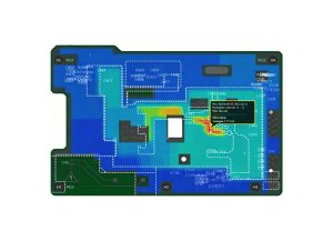
PCB power integrity focuses on ensuring that every component on a board receives clean, stable, and sufficient power under all operating conditions. Without proper power integrity design, even the most advanced circuits can suffer from noise, voltage fluctuations, or unexpected failures. This article explains what power integrity means, why it matters, and how to optimize it in real PCB designs.
EBest Circuit (Best Technology) offers comprehensive one stop electronic manufacturing services, covering electronic design support and solution development, PCB fabrication and assembly, as well as electronic component sourcing. We’re happy to support your project needs, and please feel free to contact us at sales@bestpcbs.com.
What Is Power Integrity in PCB?
Power integrity in PCB refers to the ability of the power distribution network (PDN) to deliver stable voltage and current to all devices across the board without excessive noise, ripple, or voltage drop.
In practical terms, good PCB power integrity ensures:
- Stable voltage at IC power pins
- Minimal voltage ripple and noise
- Fast transient response during switching events
- Low impedance across a wide frequency range
A well-designed PDN behaves like an ideal power source, even when load conditions change rapidly.
Why Is PCB Power Integrity Critical for High-Speed Designs?
As switching speeds increase and supply voltages decrease, circuits become more sensitive to power fluctuations. Even small voltage disturbances can cause timing errors or logic failure.
Key reasons why PCB power integrity is critical:
- Lower voltage margins: Modern ICs operate at 1V or below
- High transient currents: CPUs, FPGAs, and GPUs demand fast current bursts
- Increased switching noise: Faster edges generate more noise
- Tighter timing requirements: Small disturbances can break signal integrity
In high-speed systems, poor power integrity directly impacts:
- Signal integrity
- EMI performance
- System stability
- Product reliability
What Causes Power Integrity Issues in PCB Design?
Understanding root causes is essential for effective optimization. The most common PCB power integrity problems include:
IR Drop (Voltage Drop)
Resistance in traces, vias, and planes causes voltage loss across the PDN.
Switching Noise
Rapid current changes generate voltage fluctuations due to inductance.
PDN Resonance
Interactions between capacitors and plane inductance create resonance peaks.
Poor Decoupling Strategy
Insufficient or poorly placed capacitors fail to suppress high-frequency noise.
Ground Bounce
Shared return paths cause voltage shifts in the ground reference.
How to Perform Power Integrity Analysis in PCB Step by Step?
A structured power integrity analysis in PCB ensures predictable performance before manufacturing.
Step 1: Define PDN Requirements
- Target voltage tolerance
- Maximum allowable ripple
- Current consumption profile
Step 2: Build PDN Model
Include:
- Power planes
- Decoupling capacitors
- VRM (Voltage Regulator Module)
Step 3: Simulate Impedance Profile
Ensure PDN impedance stays below the target across frequency.
Step 4: Analyze Transient Response
Check voltage stability under dynamic load conditions.
Step 5: Optimize Layout
Adjust:
- Plane geometry
- Capacitor placement
- Via structures
What Tools Are Used for PCB Power Integrity Analysis?
Professional engineers rely on specialized tools for accurate analysis:
- Keysight ADS
- Ansys SIwave
- Cadence Sigrity
- Altium Designer
These tools allow engineers to predict issues before fabrication, reducing costly iterations.
What Are the Best Practices for Power Integrity in PCB Design?
Following proven design rules significantly improves PCB power integrity.
| Design Aspect | Recommendation | Engineering Impact |
|---|---|---|
| Power Planes | Use solid planes instead of traces | Lower impedance |
| Decoupling Capacitors | Place close to IC power pins | Reduce noise |
| Via Design | Use multiple vias for current paths | Improve current flow |
| Layer Stackup | Keep power and ground planes adjacent | Minimize inductance |
| Capacitor Selection | Use multiple values (bulk + high-frequency) | Wide frequency coverage |
How Does PDN Design Affect PCB Power Integrity Performance?
The PDN acts as the backbone of power delivery. Its design determines how effectively power is distributed.
A strong PDN design includes:
- Low inductance plane pairs
- Distributed decoupling network
- Proper capacitor hierarchy
- Short current return paths
Poor PDN design leads to:
- Voltage instability
- Increased EMI
- Reduced system lifespan
How to Solve Common PCB Power Integrity Problems Efficiently?
When issues arise, targeted fixes can quickly improve performance.
Voltage drop too high
Increase copper thickness or widen power traces
High-frequency noise
Add small-value capacitors near IC pins
PDN resonance
Adjust capacitor values to damp resonance
Ground bounce
Improve grounding and reduce shared return paths
Unstable voltage under load
Optimize VRM placement and response time
Why Choose EBest Circuit (Best Technology) for PCB Power Integrity Optimization?
Ensuring reliable power integrity in PCB design requires both simulation expertise and manufacturing experience.
At EBest Circuit (Best Technology), we provide:
- Professional engineering support
- Free DFM and PDN optimization suggestions
- Advanced simulation support for PI/SI analysis
- PCB + PCBA one-stop service
- 5-second traceability with MES system
- Fast turnaround (as short as 1.5 weeks)
Our team ensures your design performs reliably in real production environments.
FAQ About PCB Power Integrity
What is the difference between power integrity and signal integrity?
Power integrity ensures stable voltage delivery, while signal integrity focuses on accurate signal transmission. Both must be optimized together.
How do you reduce power noise in PCB?
Use proper decoupling capacitors, solid planes, and short return paths. Simulation helps identify noise sources early.
What is acceptable voltage ripple in PCB power integrity?
Typically within ±5% of nominal voltage, depending on IC requirements.
Can decoupling capacitors solve all power integrity issues?
They help significantly, but cannot replace proper PDN design and layout optimization.