PCB manufacturing PCB manufacturing
Home > Blog

Top 10 Electronic Manufacturing Services UK Companies

August 25th, 2026

If you search for electronic manufacturing services UK, you are probably not looking for another simple definition of EMS. You may already have a product, a BOM, Gerber files, an urgent prototype, a cost target, or a production issue that needs a real manufacturing partner.

UK buyers often compare local EMS companies with overseas PCB and PCBA suppliers. Local support can be valuable for close communication, fast engineering meetings, and regulated product handover. A China-based PCB and PCBA partner can also be useful when the project needs competitive cost, special PCB manufacturing, component sourcing, small-batch PCBA, DFM review, or repeat production support.

EBest Circuit (Best Technology) is not a UK local factory. We are a China-based PCB and PCBA manufacturer serving global engineers and buyers, including UK customers who need practical support from PCB fabrication to component sourcing, SMT/THT assembly, inspection, testing support, and shipment. For RFQ review, send files to sales@bestpcbs.com.

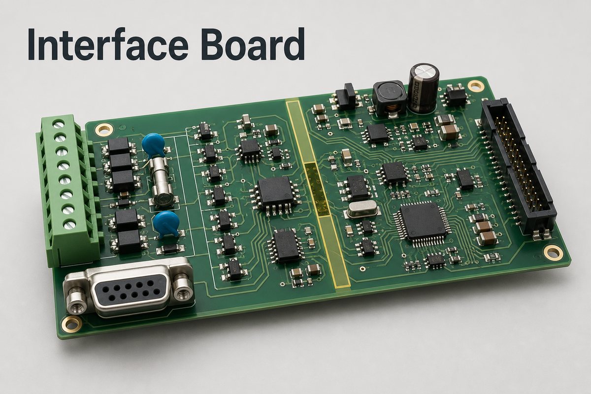
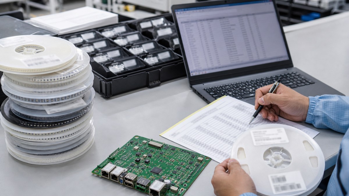
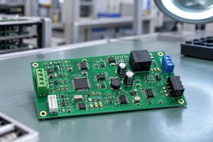
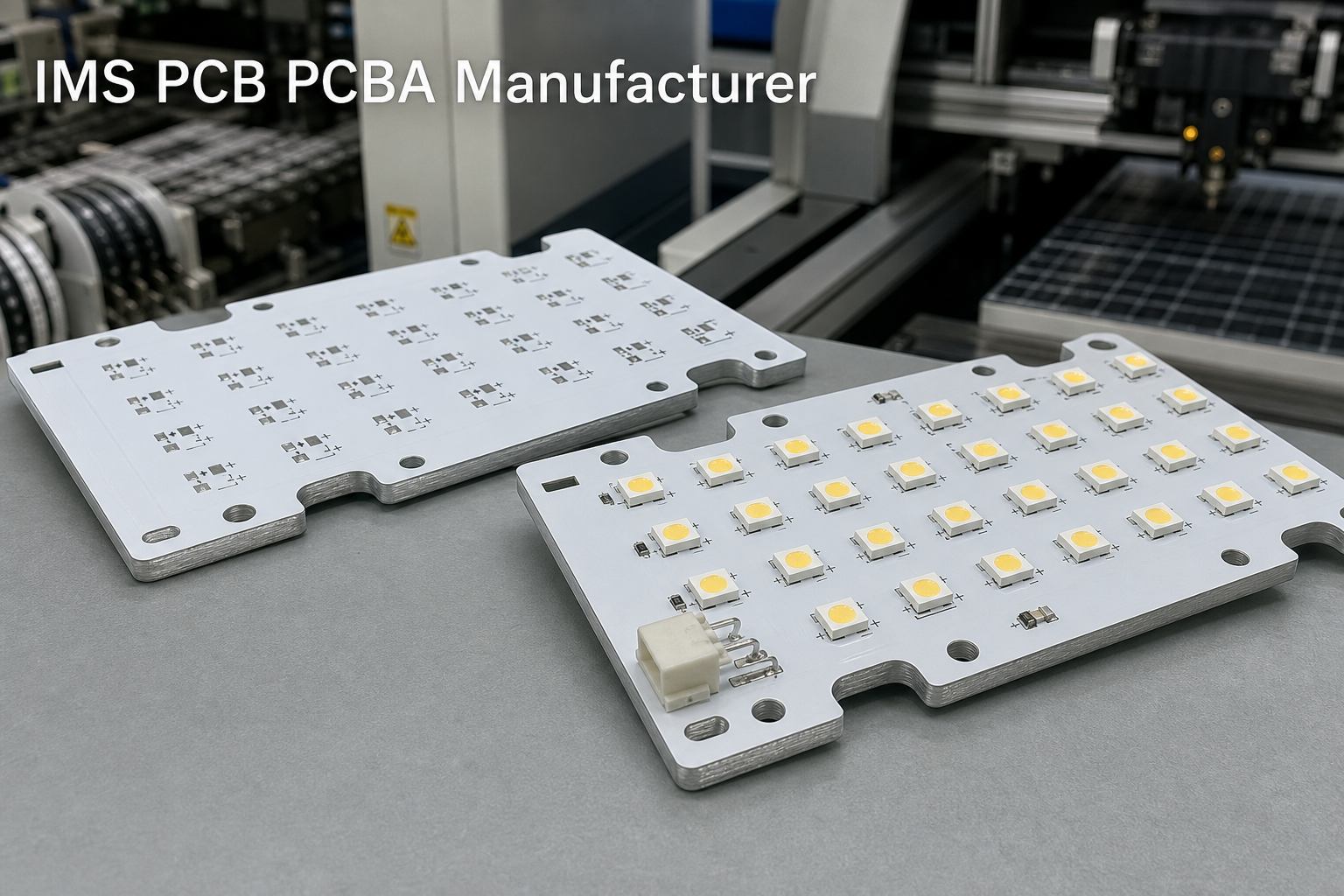
electronic manufacturing services UK
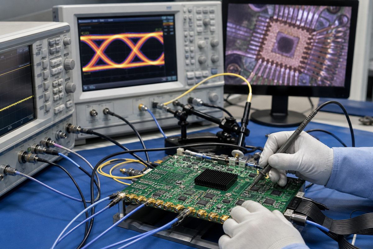
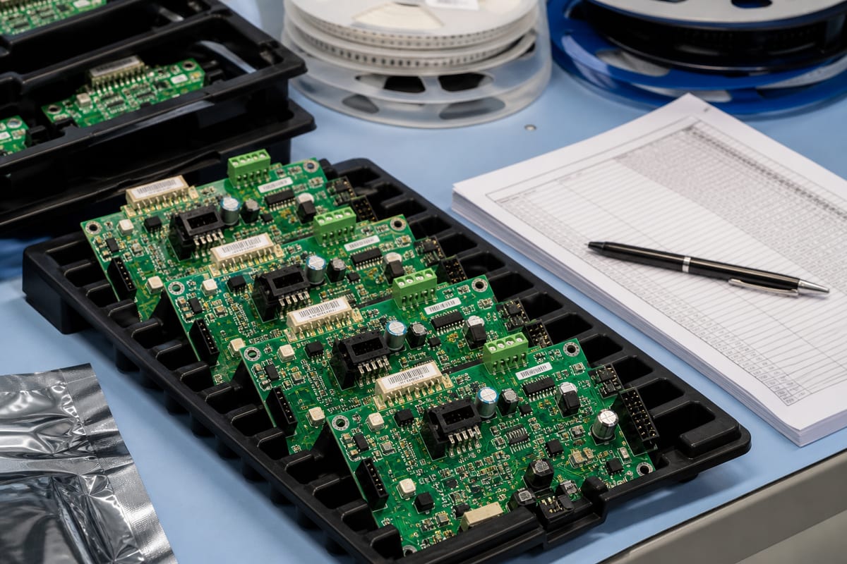
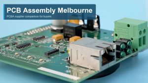
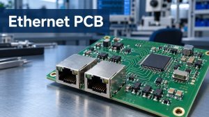
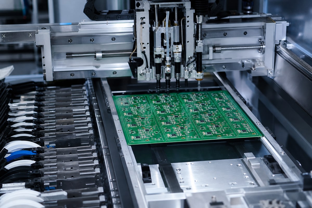
PCBA manufacturing support for UK buyers comparing EMS suppliers, cost, process capability, and delivery risk.

Top 10 Local Electronic Manufacturing Services UK Companies

A UK buyer may want a local EMS supplier for face-to-face engineering meetings, local logistics, product handover, repair support, or regulated industry communication. The companies below are useful examples to review when building a UK EMS shortlist. Always verify current capabilities, certifications, capacity, and quote scope directly before selecting a supplier.

UK EMS company Typical fit to check Buyer verification point
DSL Electronic Manufacture UK PCB assembly, box build, testing Warranty, AOI, design/manufacturing review
Protronix EMS PCB assembly, prototyping, cable assembly, turnkey EMS IPC-A-610, sourcing, traceability, production scale
Simtek EMS SMT, through-hole, full product build IPC training, AOI, industry fit
Arkle Electronics PCB assembly, cable harness, box build ISO, IPC standards, test scope
Jade Electronics High-reliability electronics manufacturing Traceability, ISO 9001, AS9100-oriented quality system
Jaltek Box build and complex electronic systems NPI, test, production transfer
EMS Technologies PCB assembly, wire harness, box build ISO 9001, AOI, production history
Active EMS Prototyping, DFM, purchasing, assembly, test Local support and supply-chain services
Active-PCB Solutions PCB assembly and EMS in Reading Conformal coating, inspection, box build
Microtech Electronics Turnkey EMS, prototypes, production, test Programming, logistics, quality control

This kind of list is only the first screen. The real decision starts when you compare quote details: what is included, what is excluded, what is tested, what is traceable, and what happens when a component or process detail changes.

UK vs China Electronic Manufacturing Services for PCBA Buyers

UK local EMS and China-based PCB/PCBA manufacturing solve different buyer problems. A local supplier may be the better choice when the project needs frequent in-person review, sensitive handover, local repair, or strict local production control. A China-based supplier can be attractive when the project needs special PCB processes, material options, component sourcing flexibility, lower unit cost, or scalable small-to-medium batch production.

A practical comparison for UK PCBA buyers:

Decision factor UK local EMS China PCB/PCBA partner
Engineering communication Easy local meetings and site visits Best when files, drawings, BOM, and test plan are clear
Prototype urgency Useful for local troubleshooting Useful when PCB, BOM, and assembly are coordinated together
Unit cost Often higher labor and overhead Often stronger for cost-sensitive repeat builds
PCB process options Depends on each local factory Strong when special PCB, MCPCB, ceramic, FPC, or rigid-flex is needed
Supply chain Local communication advantage Broad component sourcing and PCB supply-chain access
Risk control Local traceability and support Needs clear DFM, BOM review, inspection, and shipment plan

Many buyers do not choose only one model forever. They may use a UK EMS partner for early product handover and local builds, then use a China-based PCB/PCBA partner for cost-controlled prototype batches, special PCB fabrication, or repeat production. If you are comparing options, this related guide on PCB assembly UK can help you review supplier type and project fit.

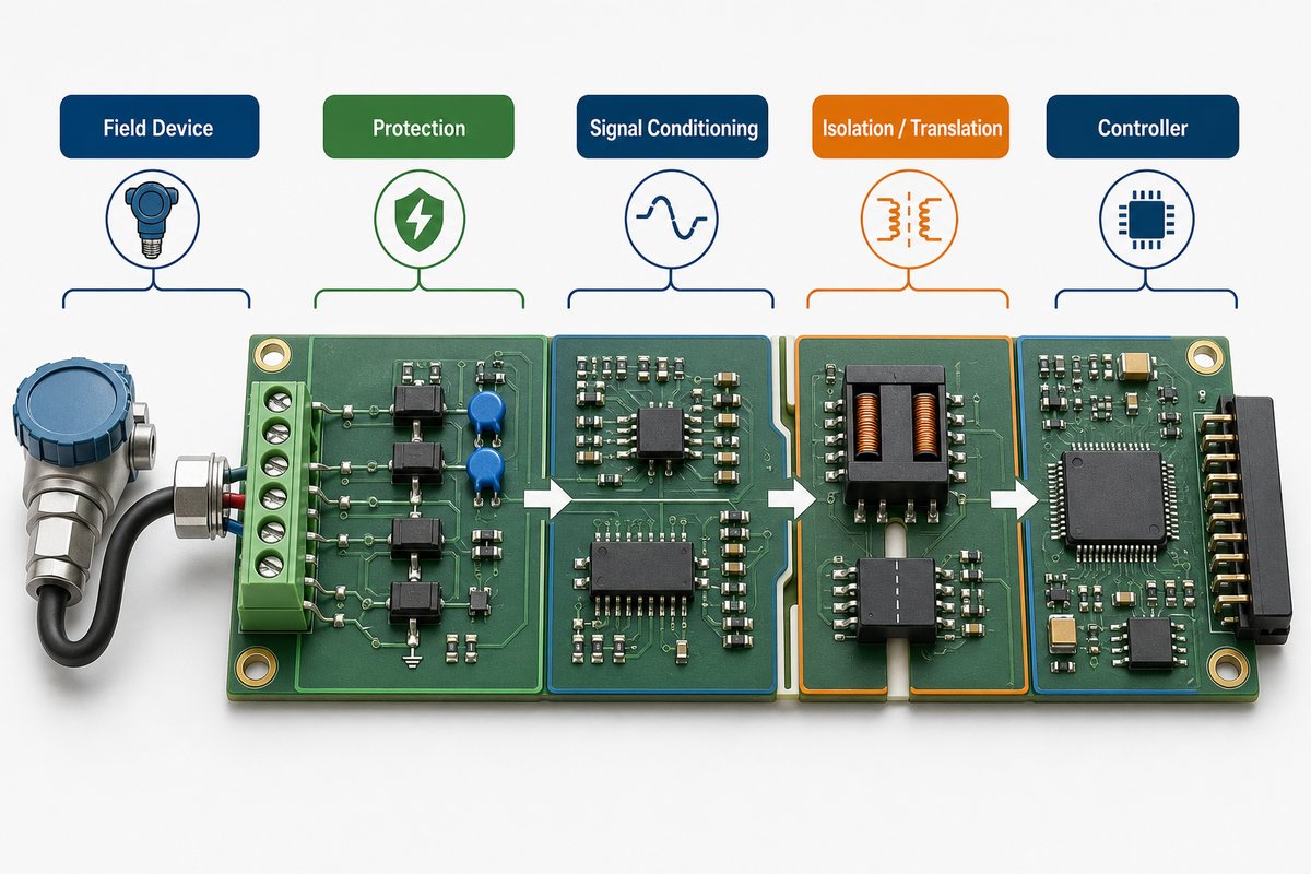
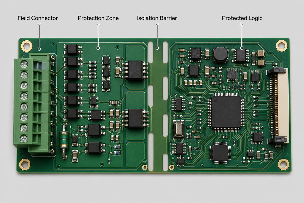
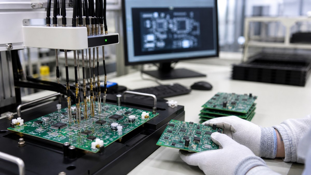
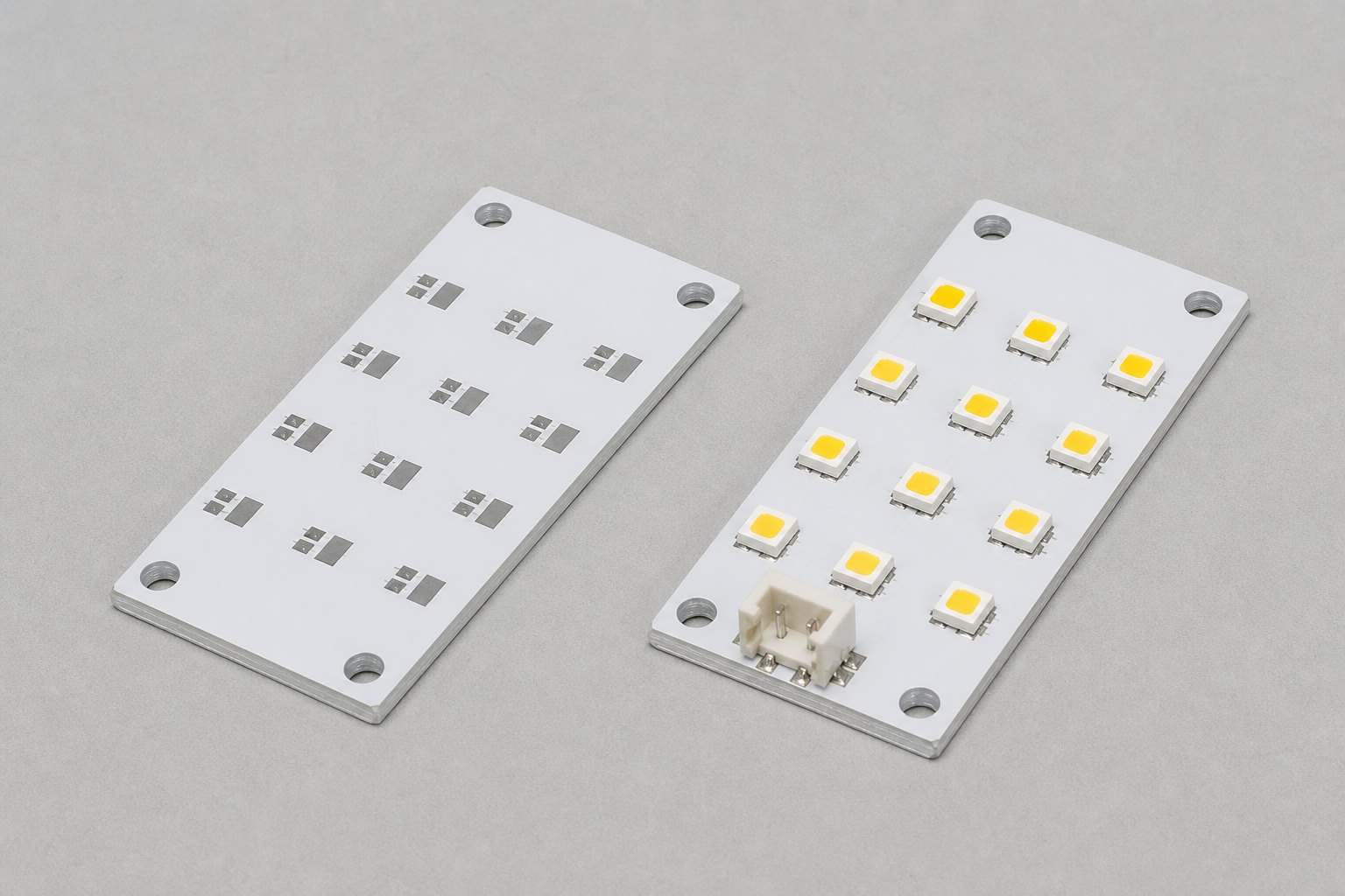
electronic manufacturing services UK
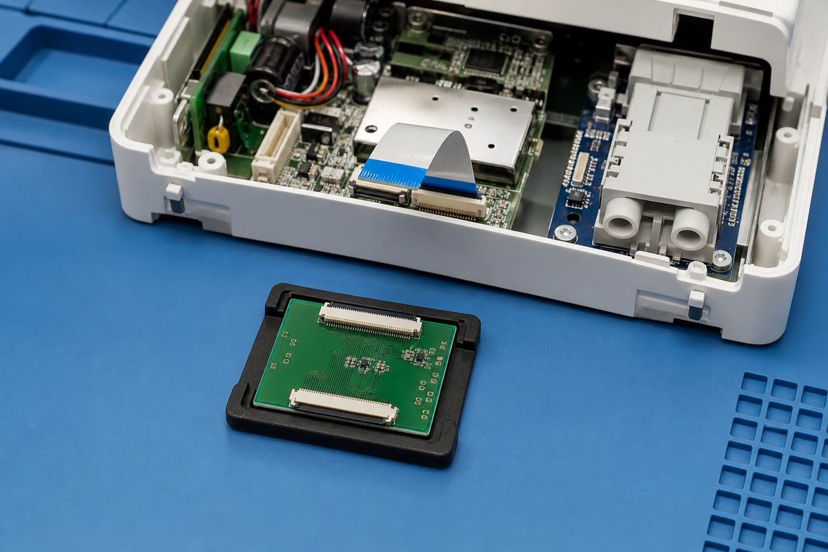
Before comparing EMS quotations, UK buyers should prepare the PCB files, BOM, drawings, quantity, test requirements, and delivery expectations.

Electronic Manufacturing Services UK Pricing: Local vs China Options

Pricing is not just the assembly unit price. A lower line-item quote can become expensive if it excludes sourcing work, test fixture preparation, engineering review, solder stencil, packaging, documentation, or failed-build risk. A higher quote may be reasonable if it includes better testing, traceability, production support, and fewer hidden handoffs.

For UK buyers, EMS pricing should be checked by total project cost:

  • PCB fabrication cost and special material cost
  • Stencil, tooling, fixture, and NPI charges
  • Component sourcing cost and shortage risk
  • SMT, THT, manual soldering, and mixed assembly labor
  • Inspection and test coverage
  • Engineering questions and DFM review time
  • Packaging, freight, customs, VAT, and landed cost
  • Cost of rework, delay, or production stoppage

A UK EMS quote may look more expensive at unit level but can reduce communication and handover risk for sensitive programs. A China PCB/PCBA quote may be more competitive for repeat builds, but it must include enough DFM review, BOM control, test support, and shipment planning to protect the project. The right comparison is not “UK price vs China price”; it is “which option gets usable assemblies into your schedule with acceptable risk?”

PCB and PCBA Process Support for UK EMS Orders from EBest Circuit

EBest Circuit supports UK EMS orders when the buyer needs a manufacturing partner that can review files, fabricate PCBs, source components, assemble boards, and support inspection or testing under one coordinated workflow. This is especially useful when the UK buyer has a clear design package but wants fewer supplier handoffs.

For a UK EMS order, EBest Circuit can support:

  • Gerber, ODB++, drill, stackup, and fabrication note review
  • DFM pre-review before production release
  • BOM review, availability check, and sourcing suggestions
  • PCB fabrication for FR4, multilayer, MCPCB, ceramic, FPC, rigid-flex, high-frequency, and special PCBs
  • SMT, through-hole, and mixed PCBA assembly
  • AOI, visual inspection, X-ray for suitable assemblies, and functional testing support
  • Prototype, small-batch, and repeat production support
  • Shipment planning for UK delivery requirements

The value is not only that one supplier can quote more items. The value is that the PCB process, BOM risk, assembly method, inspection plan, and delivery schedule can be reviewed together before the buyer places the order.

Certifications UK Buyers Can Verify Before Electronic Manufacturing Projects

Certifications do not replace project review, but they help UK buyers screen whether a supplier has a quality system suitable for the product risk. Before placing an electronic manufacturing project, buyers should ask which certifications apply to the actual factory, process, product type, and shipment documents.

EBest Circuit holds quality certifications including ISO 9001, ISO 13485, IATF 16949, AS9100D, REACH, RoHS, and UL-related support. For buyers in medical, automotive, aerospace, industrial, and controlled electronic assemblies, these certifications can help with supplier qualification before the RFQ moves into technical review.

Important certification checks include:

  • Does the certificate name match the supplier entity or factory being used?
  • Is the certificate valid during the planned production period?
  • Does the certification scope match PCB fabrication, PCBA assembly, or both?
  • Does the buyer need RoHS, REACH, UL material evidence, CoC, or test records?
  • Does the project require automotive, medical, aerospace, or other controlled documentation?

Certification is strongest when it is connected to the actual build plan: materials, approved suppliers, work instructions, inspection records, lot traceability, and final shipment documentation.

PCB and PCBA Process Capability for UK Production Builds

Production capability should be judged by what the supplier can manufacture repeatedly, not by a long capability list alone. For UK production builds, the buyer should confirm PCB type, layer count, copper requirement, board thickness, surface finish, component package, assembly method, inspection method, test plan, and order volume.

EBest Circuit provides customized PCB and PCBA support across standard and special technologies. Monthly PCB capacity is about 260,000 square feet, and more than 1,000 different board types can be completed. For assembly, the process can support SMT, through-hole, and mixed PCBA builds, including engineering review before production.
Item EBest Circuit support
PCB types FR4, multilayer, MCPCB, ceramic, FPC, rigid-flex, high-frequency, special PCB
SMT capability 01005 parts, 0.25mm BGA pitch, up to 13.2M chips/day placement capacity
Board size 0.2 x 0.2 in to 20 x 20 in; long panel support up to 22 x 47.5 in
Assembly methods SMT, THT, mixed assembly; reels, cut tape, tubes, trays, and loose parts
Engineering support DFM review, BOM sourcing, inspection, testing support, traceability

This type of capability is useful for UK buyers who do not want to split PCB fabrication, component sourcing, and PCBA across too many vendors. It also helps when the design includes special PCB materials, non-standard stackups, or mixed assembly requirements.

Lead Time Support for UK PCBA Prototype and Production Orders

Lead time is one of the main reasons UK buyers compare EMS suppliers. The schedule is not controlled only by assembly speed. It depends on file readiness, PCB technology, component availability, stencil preparation, DFM closure, engineering questions, test preparation, production capacity, packing, freight, and customs.

Lead time should be planned by the bottleneck, not by the fastest process step:

Build type Typical planning window Fastest support when suitable
Standard FR4 prototypes, 1-4 layers 7-10 days 24-48 hours
Higher-layer FR4, 6-8 layers 10-12 days About 72 hours
1-layer MCPCB prototypes About 4 days About 24 hours
Special PCB builds Usually planned by stackup and material Confirmed after engineering review
PCBA after materials are ready 1-5 days assembly window Urgent suitable builds can be faster

For suitable PCBA projects, EBest Circuit can support fast delivery, including around 1.5-week PCBA turnaround when project files, materials, engineering conditions, and production capacity are ready. This is useful for UK prototype validation, small-batch builds, and urgent production support. It should still be confirmed case by case before the buyer commits the customer delivery date.

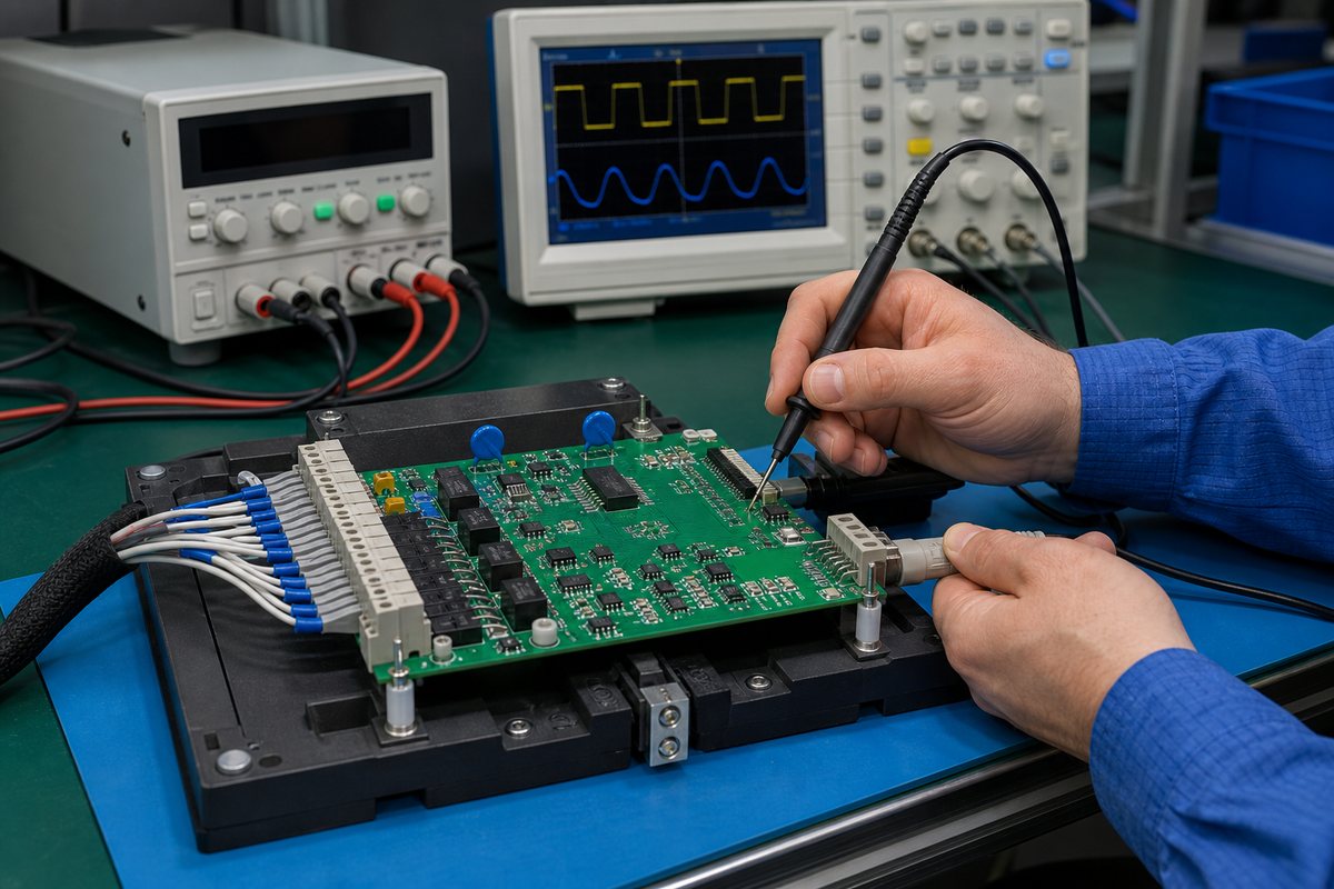
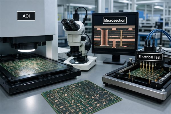
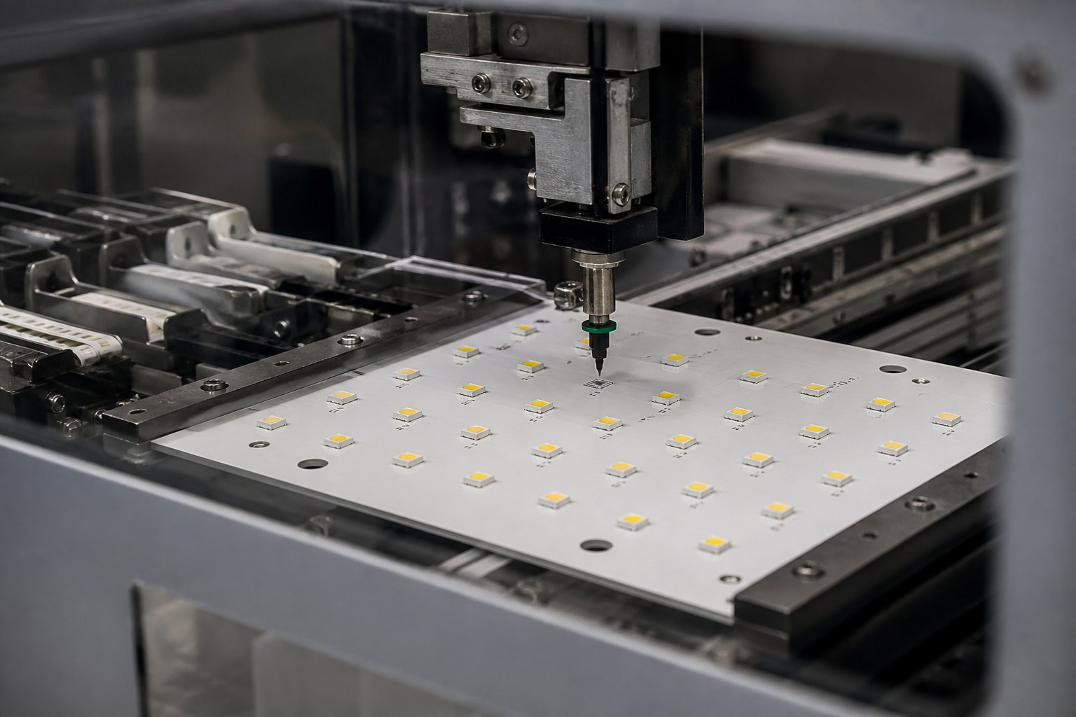
electronic manufacturing services UK
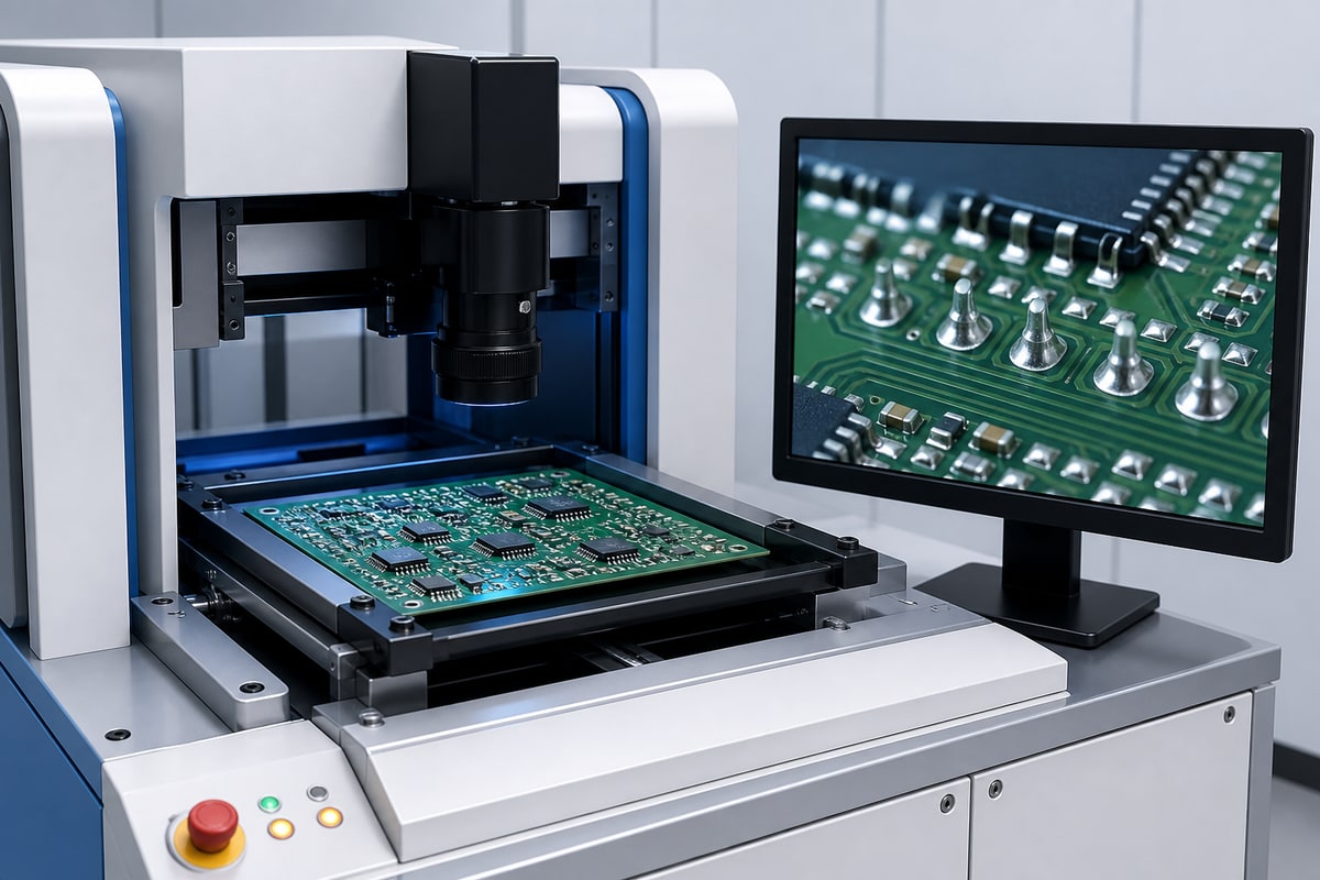
Inspection and functional testing preparation help protect UK PCBA prototype and production schedules.

UK PCBA Project Case Study with EBest Circuit Support

A UK industrial automation buyer contacted EBest Circuit for a small-batch PCBA project after the first local quotation exceeded the target budget. The product was a control module used inside an equipment cabinet. The buyer needed a repeatable build, not only a few prototype boards.

Project requirements:

  • Country: United Kingdom
  • Application: industrial control module for equipment monitoring
  • PCB type: 4-layer FR4 control board with mixed SMT and through-hole connectors
  • Quantity: 50 pcs prototype validation, then 300 pcs pilot order
  • Buyer concern: BOM risk, connector orientation, test access, and schedule control
  • Required support: PCB fabrication, component sourcing, SMT/THT assembly, inspection, and functional test preparation

Main challenges:

  • Two connector footprints had similar bodies but different pin directions.
  • Several ICs had alternative part numbers with different lead times.
  • The original test pads were too close to the enclosure edge.
  • The buyer wanted a pilot batch quickly, but the BOM was not fully locked.

EBest Circuit solution:

  • Our engineering team reviewed Gerber, BOM, centroid, and assembly drawings before quotation finalization.
  • The BOM sourcing team marked long-lead and alternative parts for buyer approval.
  • The DFM review flagged connector orientation and test-point access before PCB release.
  • SMT and THT assembly were planned in one sequence to reduce rework risk.
  • Inspection and functional test preparation were aligned before pilot production.

The result for the buyer was a clearer production path: one supplier managed PCB fabrication, component sourcing, PCBA assembly, and inspection communication. The project still required buyer approval for alternatives and test details, but the RFQ moved from a simple price comparison to a controlled build plan.

Why UK Buyers Choose EBest Circuit for PCB and PCBA Manufacturing

UK buyers choose EBest Circuit when they need more than a bare PCB quote. Many projects require a supplier that can review the manufacturing files, catch assembly risks, source components, support special PCB types, and help the project move from prototype to repeatable production.

EBest Circuit is a practical option when UK buyers need:

  • One-stop PCB fabrication, component sourcing, PCBA assembly, and testing support
  • DFM pre-review and BOM optimization before production
  • Support from 1 business representative and 3 engineers through the project flow
  • Manufacturing input from engineers with long PCB and PCBA experience
  • Prototype and small-batch support for design validation
  • ISO 9001, ISO 13485, IATF 16949, AS9100D, REACH, RoHS, and UL-related quality support
  • Own PCB and PCBA factory resources plus a 1,000+ supplier network
  • Digital workshop traceability for material, batch, production cycle, and production progress

For buyers who are still defining the service scope, this article on EMS manufacturing explains the wider manufacturing model. If the project includes UK-specific supplier comparison, related topics such as PCB manufacturer UK and flexible PCB manufacturer UK may also help buyers screen options before sending the RFQ.

FAQs About Electronic Manufacturing Services UK Companies

Should UK buyers always choose a local EMS company?

No. A local EMS company can be valuable for face-to-face communication, regulated product handover, or local service support. A China-based PCB/PCBA partner can be better when the buyer needs special PCB processes, competitive cost, sourcing flexibility, or small-batch manufacturing support.

What files should I send for an EMS quotation?

Send Gerber or ODB++ files, BOM, centroid or pick-and-place file, assembly drawings, quantity, surface finish, test requirements, delivery destination, and any special packaging or inspection requirements. Clear files reduce quote delay and engineering questions.

Can EBest Circuit support both PCB fabrication and PCBA assembly?

Yes. EBest Circuit supports PCB fabrication, component sourcing, SMT assembly, through-hole assembly, mixed assembly, inspection, and testing support. This is useful when UK buyers want fewer handoffs between PCB supplier, component supplier, and assembly supplier.

How should UK buyers compare EMS quotations?

Compare total delivered value, not only unit price. Check PCB cost, BOM sourcing, assembly labor, tooling, test fixture, inspection records, delivery schedule, freight, customs, and the cost of delay or rework.

What makes an EMS supplier reliable for repeat production?

A reliable supplier should control BOM sourcing, approved alternatives, DFM records, process flow, inspection method, test plan, lot traceability, packaging, and delivery communication. Repeatability matters more than a low first quote.

In Conclusion, electronic manufacturing services UK buyers should compare local EMS companies and China-based PCB/PCBA partners by cost, process capability, certifications, lead time, risk control, and production repeatability. If you need PCB fabrication, component sourcing, PCBA assembly, DFM review, inspection, or testing support for a UK project, contact EBest Circuit (Best Technology) at sales@bestpcbs.com.

You may also like

ABF Substrate Shortage in 2026: Supply, Price and Delivery Risks

August 25th, 2026

The ABF substrate shortage is becoming a high-end AI packaging constraint rather than a broad shortage affecting every substrate equally. Counterpoint Research estimated an ABF supply gap of about 10% in the second half of 2026, widening to 20% in 2027 before new capacity comes online.

The risk is concentrated in large, multilayer package substrates that consume more low-CTE glass cloth, ABF dielectric, semi-additive-process capacity, and inspection time. Buyers should qualify the exact package construction and supplier allocation instead of treating the forecast as a universal lead-time or price increase.

3D cutaway of a high-end AI processor on an ABF package substrate

What Is Causing the ABF Substrate Shortage?

The shortage is being driven by rapid AI-package growth, larger substrate area, higher layer counts, constrained low-CTE T-glass, and the slow ramp of qualified high-end capacity. These pressures reduce the number of advanced packages that an existing line can produce even when the nominal panel count looks unchanged.

Counterpoint Research described a structural up-cycle tied to enterprise AI demand and estimated that one AI chip can consume roughly ten times the substrate material of a standard PC chip. That is an industry estimate, not a design rule for every package, but it explains why mix shift matters as much as unit demand.

What Is ABF Substrate Material and Film?

ABF substrate material is an organic build-up system used to route very fine connections between a high-performance semiconductor die and the larger-pitch PCB below it. ABF substrate film is the interlayer dielectric used between copper routing layers; laser processing and direct copper plating help form the dense interconnect structure.

Ajinomoto explains that ABF combines organic epoxy chemistry with inorganic microparticle filler to provide insulation, low thermal expansion, durability, and processing characteristics for advanced package substrates. The film is one part of a complete substrate that also includes copper circuitry, a core or coreless structure, vias, solder mask, surface finish, and BGA connections.

Macro cross-section of a multilayer ABF package substrate beneath an AI processor

How Large Is the 2026–2027 Supply Gap?

The current public forecast points to a roughly 10% ABF gap in the second half of 2026 and a 20% gap in 2027. These figures should be treated as analyst estimates for the industry, not guaranteed shortages for every supplier, package type, or customer contract.

Period Public Signal Buyer Interpretation
H1 2026 3–5% quarter-over-quarter substrate price increases expected Quotes may be revised as material and capacity costs move
H2 2026 About 10% ABF supply gap forecast High-end allocation and schedule risk become more visible
2027 Gap forecast to widen to about 20% New capacity starts, but demand and qualification may outpace ramp
From FY2027 IBIDEN plans sequential new mass-production capacity Capacity relief depends on equipment, qualification, yield and customer mix

Why Does Low-CTE T-Glass Matter?

Low-CTE T-glass helps control dimensional stability and warpage in large, thin, multilayer organic packages. As package size and layer count increase, the substrate must survive lamination, thermal cycles, assembly, and operation while keeping fine features aligned.

Counterpoint estimated a T-glass supply-demand gap above 10% in 2026. A shortage of qualified glass cloth can restrict both ABF substrate output and high-end copper-clad laminate, even if a substrate manufacturer has available imaging, plating, and drilling equipment. An alternate glass style is not automatically interchangeable; resin compatibility, thickness, CTE, electrical properties, process behavior, and package reliability must be validated.

How Do Larger AI Packages Consume More Capacity?

Larger AI packages consume capacity through area, layer count, process steps, inspection burden, and yield—not just unit volume. More build-up layers require repeated lamination, laser-via formation, desmear, metallization, imaging, plating, etching, and inspection cycles.

  • More substrate area: fewer units may fit on a panel, and each defect affects more value.
  • More routing layers: repeated build-up cycles occupy equipment for longer.
  • Finer features: tighter process windows raise inspection and yield demands.
  • Warpage control: larger packages need more precise material and process matching.
  • Embedded or advanced structures: additional failure points can reduce effective output.

IBIDEN’s 2026 results presentation indexed the production load for an AI-server substrate at 1.8 times its 2024 level in 2026 and 2.5 times in 2028 when converted by semi-additive-process demand.

Which Price and Lead-Time Signals Matter?

The most useful signals are configuration-specific quotes, allocation confirmation, material status, committed capacity, qualification status, and delivery milestones. Broad market percentages do not replace a supplier’s documented production plan.

Signal What to Request Decision Use
Material allocation ABF film, glass cloth, core and copper availability by construction Tests whether the quoted stack is actually supported
Qualified capacity Committed line, approved process and customer qualification status Separates installed equipment from usable output
Price validity Validity period and material-adjustment mechanism Defines exposure between quote and release
Milestones Material receipt, start, inspection, shipment and recovery dates Provides an auditable schedule
Yield assumptions Sampling, inspection and disposition rules Shows how defects could affect delivery

How Are ABF Substrate Manufacturers Expanding Capacity?

ABF substrate manufacturers are investing heavily, but high-end capacity takes time to install, qualify, and stabilize. IBIDEN announced an approximately JPY 500 billion investment plan for FY2026–FY2028, focused on high-performance IC package substrates for AI and high-performance servers, with sequential operation and planned mass production beginning in FY2027.

IBIDEN also stated that larger and more multilayered substrates are expected to push total semi-additive-process demand beyond industry supply capacity. Buyers should therefore distinguish a capital-spending announcement from qualified volume that is available to their exact package and schedule.

High-end package substrate production and optical inspection line

What Should Buyers Ask ABF Substrate Suppliers?

ABF substrate suppliers should answer against the exact package construction, not only a generic product family. A useful sourcing review covers materials, manufacturing site, qualified process, capacity commitment, inspection, change control, and recovery planning.

  • Which ABF film grade, glass style, core construction, and copper system are quoted?
  • Are all materials allocated for the requested prototype and production quantities?
  • Which site and production line are qualified for this package?
  • What changes require customer notification and requalification?
  • How are warpage, layer registration, microvias, copper thickness, continuity, and surface defects inspected?
  • What is the recovery plan if material or yield misses the committed milestone?

For terminology and structure differences, see our IC substrate overview and guide to IC substrate types and materials.

How Does the Shortage Affect PCBA Planning?

The substrate shortage can delay packaged processors before those components ever reach the PCBA line. A PCB assembler may have bare boards, passive components, and production capacity ready while waiting for the processor or accelerator package.

Project plans should link package delivery milestones to PCB fabrication, component kitting, stencil release, assembly slots, firmware readiness, and test-fixture availability. Avoid building a schedule that assumes every upstream item will arrive on the same day. The distinction between a BT substrate and a high-end ABF substrate also matters because material allocation and package applications differ.

Which Design and Qualification Actions Reduce Risk?

Risk falls when the team freezes the package interface early, keeps alternates evidence-based, and plans qualification before a shortage forces a change. Late substitutions are especially dangerous when they alter substrate dimensions, ball map, electrical behavior, warpage, thermal path, or assembly profile.

  1. Freeze the package outline, ball map, PCB land pattern, keep-outs, and thermal interface.
  2. Record the approved substrate construction and material set.
  3. Qualify alternates before allocation becomes critical.
  4. Align substrate, component, PCB, assembly, and test milestones in one schedule.
  5. Define incoming inspection, traceability, change notification, and nonconformance handling.
ABF film, glass cloth and package substrate materials under supply review

FAQ About ABF Substrate Shortage

Is every ABF substrate in shortage?

No. The pressure is strongest in high-end, large, multilayer substrates for AI and advanced computing. Supplier allocation, construction, customer qualification, and contract status determine the actual risk.

What is the difference between ABF film and an ABF substrate?

ABF film is the insulating build-up dielectric. The finished substrate combines that dielectric with copper circuitry, vias, a core or coreless structure, solder mask, surface finish, and package connections.

Why does new factory capacity not solve the shortage immediately?

Equipment installation is only one step. Materials, process qualification, customer approval, yield ramp, inspection capacity, and product mix determine when usable output becomes available.

Will substrate prices rise by the same percentage for every buyer?

No. Public percentages are market estimates. The actual change depends on package size, layers, materials, committed capacity, order volume, contract terms, timing, and supplier relationship.

Can a PCB fabricator replace an ABF package substrate?

Not directly. An advanced IC package substrate uses different feature sizes, processes, materials, equipment, quality controls, and semiconductor-package qualifications from a conventional PCB.

How Can EBest Circuit Support Substrate and PCB Planning?

EBest Circuit supports PCB design, PCB fabrication, component sourcing, PCB assembly, prototyping, mass production, and engineering review. For projects exposed to package-substrate constraints, send us the Gerber files, BOM, stack-up, package details, quantities, approved alternates, testing requirements, and target schedule. We can review the downstream PCB and PCBA plan and provide a project-specific quotation at sales@bestpcbs.com.

You may also like

AI Server Price Increase in 2026: What Buyers Should Budget for 2027

August 25th, 2026

The AI server price for some Grace Blackwell and Vera Rubin systems shipping in early 2027 may rise by more than 15%, according to a Bloomberg report based on private customer communications. This is not a universal NVIDIA price list. The final change depends on platform generation, memory configuration, rack content, commercial terms, and delivery timing.

For buyers, the practical issue is wider than the accelerator. Memory, high-layer PCBs, power delivery, cooling, networking, packaging substrates, and component allocation can all change the delivered rack cost or schedule. A useful 2027 budget therefore needs a configuration baseline, an evidence-based bill of materials, and separate allowances for volatile and fixed-cost items.

3D AI server rack and compute tray illustrating AI server price drivers

What Does the Reported 15% AI Server Price Increase Cover?

The reported increase applies to many, but not necessarily all, systems containing NVIDIA AI chips that are scheduled to ship in early 2027. Bloomberg reported that affected configurations include Grace Blackwell and Vera Rubin systems and that the percentage varies with chip generation and memory content.

That distinction matters. A rack-level quote may combine compute trays, switching, storage, cooling distribution, power shelves, commissioning, support, and integration. Buyers should not apply a flat 15% multiplier to every server or infer that NVIDIA has published a standard increase for every SKU. Treat the figure as a reported commercial signal and request a configuration-specific quotation.

Why Are AI Server Prices Rising?

Memory inflation is the clearest near-term driver, while constrained server components and more complex rack architectures add pressure elsewhere. TrendForce forecast server DRAM contract prices to rise 13–18% quarter over quarter in Q3 2026 and expected continued quarterly increases into 2027, although long-term agreements may limit changes for some large customers.

  • HBM and server DRAM: higher capacity per system and tight supply increase the memory share of the bill of materials.
  • Accelerators and CPUs: platform generation, allocation, packaging, and contract timing affect the compute cost.
  • High-speed networking: switches, optical modules, NICs, retimers, and cables scale with cluster topology.
  • Power and cooling: higher rack density requires larger power shelves, liquid-cooling hardware, monitoring, and facility work.
  • PCBs and substrates: larger boards, more layers, lower-loss materials, tighter impedance control, and advanced packages consume constrained production resources.

AI Server Cost Breakdown: Which Parts Move the Quote?

An AI server cost breakdown should separate configuration-driven cost from market-driven cost. That makes price comparisons more useful and prevents a lower headline quote from hiding omitted memory, networking, cooling, or qualification work.

Cost Group What Changes the Cost Quote Evidence
Compute and memory GPU/CPU generation, accelerator count, HBM capacity, system DRAM Exact part numbers, capacity, quantity, allocation status
PCB and PCBA Board size, layer count, laminate, impedance, copper, assembly complexity Gerber, stack-up, BOM, fabrication notes, test plan
Networking Fabric type, port speed, switch count, optics and cabling Topology and approved component list
Power and cooling Rack power, redundancy, liquid loop, cold plates and facility interface Power budget, thermal design and included hardware
Integration and support Burn-in, firmware, installation, warranty and service scope Acceptance criteria and service statement
Exploded AI server compute tray showing PCB, memory, power and cooling cost drivers

How Should Buyers Read an AI Server Price List?

An AI server price list is only comparable when every line uses the same scope, currency basis, delivery term, support period, and configuration date. Online prices often describe a base chassis or workstation, while rack-scale platforms are usually quoted against a detailed deployment specification.

  1. Confirm whether the number covers a node, tray, rack, pod, or complete cluster.
  2. Match accelerator model, count, memory capacity, CPU, storage, and network interfaces.
  3. Identify excluded items such as optics, coolant distribution, power equipment, installation, tax, and freight.
  4. Record quote validity, allocation status, delivery window, and price-adjustment clauses.
  5. Compare total deployed cost, not only the hardware subtotal.

How Does an AI Server PCB Shortage Affect Delivery?

An AI server PCB shortage can delay assembly even when accelerators are allocated, because the compute tray cannot be completed without qualified high-layer boards, power boards, backplanes, and control boards. TrendForce reported that lead times for some server PCBs and CPUs had extended to nearly one year, with PMIC and BMC lead times also lengthening.

High-end server boards are difficult to substitute late. A laminate change, stack-up change, impedance deviation, or alternate fabricator can trigger signal-integrity, power-integrity, thermal, mechanical, and compliance revalidation. Buyers should separate supplier capacity confirmation from a generic material-availability statement.

What Changes in AI Server PCBA Planning?

An AI server PCBA program needs earlier design freeze and tighter control of alternates than an ordinary commercial assembly. The BOM contains high-current power devices, dense connectors, retimers, clocks, controllers, memory-related components, and thermal interfaces that may each have different allocation and qualification constraints.

EBest Circuit recommends releasing the manufacturing package with the Gerber files, BOM, approved stack-up, quantity, test requirements, and substitution rules. Our AI server PCB design guidance explains the routing, power, thermal, and manufacturability questions that should be settled before the production quote is treated as firm.

Engineers reviewing an AI server PCB, stack-up and component cost data

Which Costs Should Be Locked Before a 2027 Deployment?

Lock the configuration, approved sources, commercial adjustment rules, and acceptance scope before treating a 2027 budget as committed. A single lump-sum contingency is less useful than separate risk bands for memory, compute, PCB/PCBA, networking, cooling, logistics, and integration.

Decision What to Freeze Why It Matters
System configuration Platform generation, tray count, memory, storage, network Prevents scope drift between budget and order
PCB package Gerber, stack-up, laminate, impedance and fabrication notes Reduces late redesign and requalification
BOM control MPNs, approved alternates, lifecycle and allocation status Separates qualified options from unapproved substitutions
Commercial terms Quote validity, deposits, adjustment formula and cancellation Defines which inflation risk each party carries
Acceptance Inspection, electrical test, functional test and documentation Prevents a low quote from excluding required verification

How Can Procurement Compare Quotes Without Hiding Risk?

Procurement should normalize every quote into the same configuration and evidence checklist. If one supplier includes memory allocation, optics, liquid-cooling hardware, burn-in, and freight while another excludes them, the totals do not describe the same purchase.

  • Ask which prices are fixed, indexed, provisional, or subject to allocation.
  • Require the date and source of component availability evidence.
  • Separate NRE, tooling, qualification, prototype, and recurring production cost.
  • Confirm whether alternates require written approval.
  • Request traceability and incoming-inspection records for high-risk components.

For component-heavy programs, our component sourcing process provides a practical framework for BOM review and supply evidence.

What Should Engineering Freeze Before Placing an Order?

Engineering should freeze the interfaces that would force a new PCB or system validation cycle if changed. These include board outline, connector locations, stack-up, controlled impedance, power rails, thermal interfaces, firmware dependencies, test points, and approved component substitutions.

A completed AI server PCB RFQ should therefore include Gerber or ODB++ data, drill files, stack-up, impedance requirements, BOM, assembly drawings, quantities, test requirements, and target schedule. If the server platform is still changing, identify the unstable interfaces instead of asking a supplier to price an undefined production configuration.

Procurement and quality staff inspecting AI server PCBs and components

FAQ About AI Server Price and Supply

Are all AI server prices increasing by more than 15%?

No. The figure is a reported increase for many affected Grace Blackwell and Vera Rubin systems shipping in early 2027, not a public universal price schedule. Configuration and contract terms determine the actual change.

Is memory the only reason AI servers cost more?

No. Memory is a major current driver, but accelerators, CPUs, high-speed networking, advanced packaging, high-layer PCBs, power delivery, liquid cooling, integration, and facility work also affect the deployed cost.

Can a buyer use an online AI server price as a rack budget?

Only after confirming the scope. Online prices may exclude accelerators, optics, cooling, power equipment, support, freight, tax, installation, or cluster networking.

Why can a PCB delay hold up a complete AI rack?

The compute tray, backplane, power boards, and controllers depend on qualified PCB stack-ups and components. A late material or supplier change may require electrical, thermal, mechanical, and manufacturing revalidation.

What files improve an AI server PCB or PCBA quote?

Provide Gerber or ODB++ data, drill files, stack-up, controlled-impedance requirements, BOM, assembly drawings, quantities, test requirements, substitution rules, and the requested delivery schedule.

How Can EBest Circuit Support AI Server PCB and PCBA Planning?

EBest Circuit supports PCB design, PCB fabrication, component sourcing, PCB assembly, prototyping, mass production, and engineering review. For an AI server program, send us the Gerber files, BOM, stack-up, quantities, controlled-impedance needs, testing requirements, and delivery target. We can review the manufacturing package and provide a configuration-specific quotation at sales@bestpcbs.com.

You may also like

PCB Panelization Approval: Prevent Costly Production Changes

August 25th, 2026

A PCB panelization drawing is not just a convenient way to place several boards on one manufacturing panel. It defines how the boards will be fabricated, handled, assembled, separated, counted and delivered. If those decisions are left unclear, a technically correct PCB can still require a new quotation, a revised fixture, manual handling or a last-minute production change.

The practical goal is simple: approve the panel before it becomes a production constraint. This guide helps PCB engineers and buyers decide who should create the array, what the manufacturer needs to review, and which details must be frozen before fabrication and assembly begin.

panelization
Review the PCB panel, production drawing and delivery format before production approval.

What Should Be Confirmed Before PCB Panelization?

Panelization should begin with the required production and delivery flow—not with a target number of boards per panel. Before a panel drawing is created, confirm the following points.

  • Required delivery unit: Will the supplier deliver individual PCBs, complete panels or assembled boards separated after SMT?
  • Single-design or mixed panel: Will every position contain the same design, or must several part numbers share one panel?
  • Quantity basis: Is the order and quotation based on individual pieces or complete panels?
  • Downstream process: Will the panel pass through solder paste printing, pick-and-place, reflow, AOI, functional testing or another fixture-dependent process?
  • Allowed panel changes: May the fabricator rotate boards, change the up count or adjust the rails to improve manufacturability?
  • Depaneling responsibility: Will separation occur at the PCB factory, PCBA factory or customer site?
  • Quality rules: Are X-outs allowed? Are panel-level traceability, coupons, electrical testing or special packaging required?

These answers create the design boundary. Without them, two suppliers can interpret the same Gerber package differently and return quotations that do not cover the same deliverable.

The board construction also matters. A standard FR4 PCB may allow several practical layouts, while a thin flexible circuit, brittle ceramic substrate, heavy-copper board or impedance-controlled multilayer design can impose additional handling and process limits.

Who Should Control the Panelization Design?

Who should control the layout depends on the equipment and downstream processes the panel must fit.

Let the PCB manufacturer create the panel when:

  • You are supplying a single-board Gerber package.
  • The main objective is manufacturability and material utilization.
  • No customer-owned pallet, stencil or assembly fixture fixes the panel dimensions.
  • The manufacturer may adjust rails, spacing and orientation within agreed limits.

In this situation, send the finished board data and the required delivery conditions. The fabricator can propose a production panel based on its process and working-panel format. You should still review the production drawing before release.

Supply or control the array when:

  • A stencil, carrier, test fixture or automated line already depends on a fixed outline.
  • Several different boards must be delivered as one matched set.
  • Board orientation is controlled by a connector, sensor, coating or assembly requirement.
  • The panel must match an approved repeat-order configuration.
  • Traceability or packaging is managed at panel level.

The safest handoff is a documented division of responsibility. The customer defines the functional and downstream constraints, while the manufacturer confirms that the proposed panel can be fabricated, assembled and separated without creating avoidable risk.

Do not assume that an old panel should automatically be reused. A change in laminate, copper weight, board thickness, component placement, assembly site or delivery format can make the previous array unsuitable even when the circuit revision appears minor.

How Should PCB Panelization Methods Match the Board?

The best separation method is the one that fits the board outline, component layout, material and downstream handling—not simply the least expensive cutting process.

  • V-scoring is usually considered when boards have straight shared edges and can be arranged in rows. It can support efficient separation, but the score line and remaining web must be reviewed against board thickness, copper distribution and nearby components. Components, solder joints and brittle features should not be placed where bending during separation can transfer damaging stress.
  • Tab routing is useful for irregular outlines or layouts that cannot share continuous straight edges. Routed gaps define most of the finished profile, while tabs keep each board connected to the array. Tab position, width and removal method should be agreed before production. Poorly positioned tabs can leave difficult edge cleanup or transfer force toward sensitive areas.
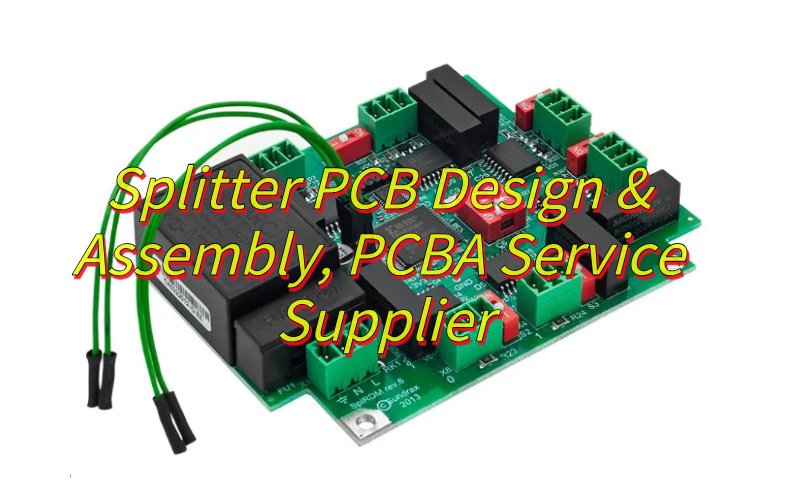
  • Mouse-bite perforations can make manually removed tabs easier to break, but hole size, pitch and distance from the finished edge affect the remaining witness marks. If the enclosure requires a smooth edge, secondary finishing or a different tab strategy may be needed.
  • Mixed-design panels may reduce handling for matched products, but they require additional control. The designs must be compatible in material, thickness, copper build, surface finish, process route and delivery quantity. Combining unrelated boards only to fill open space can complicate fabrication, assembly and quality disposition.

Special constructions require more than a generic rectangular array:

  • A rigid flex PCB may need temporary support and careful control of the flexible areas.
  • A ceramic PCB is brittle, so separation force and edge damage need particular attention.
  • Heavy-copper and asymmetrical multilayer boards may require warpage review.
  • Thin boards and FPCs may depend on tooling or carriers for stable assembly handling.
  • Impedance-controlled boards require the approved stackup and coupon strategy to remain aligned with the production panel.

This is why PCB panelization methods should be selected after the manufacturer reviews the actual build—not copied from a visually similar board.

panelization
V-scoring and routed breakaway tabs must match the board outline, material and separation requirements.

How Do PCB Panel Size and Array Quantity Affect Cost?

More boards per panel do not automatically mean a lower total cost. The better question is whether the selected PCB panel size creates a stable, repeatable route through fabrication and assembly.

The real panel cost is influenced by:

  • The usable manufacturing area and required process margin.
  • Board outline, rotation and spacing.
  • Rail width and routing channels.
  • Tooling holes, fiducials, coupons and identification areas.
  • Material type, copper weight, layer count and stackup.
  • Fabrication yield and the policy for defective units within a panel.
  • SMT line limits, stencil dimensions and fixture size.
  • Whether the supplier ships by piece or by complete panel.

For example, increasing an array from four boards to six may improve laminate utilization, but it can also make the panel less rigid, exceed an assembly-line limit or increase the commercial impact of one rejected panel. Conversely, an array with generous unused space may be justified when it provides the rails, support and keep-outs required for stable processing.

Buyers should request a quotation that states:

  • Finished board size.
  • Proposed panel size.
  • Number of boards per panel.
  • Number of panels and total good-board quantity.
  • Whether X-outs are permitted.
  • Whether the price includes depaneling.
  • Whether assembly and final delivery are quoted per panel or per finished board.

This removes a common source of price confusion: two quotations may show the same piece quantity while assuming different panel counts, separation work or acceptable panel yield.

How Should Panel Design Support Assembly and Depaneling?

A fabrication-efficient array can still be inconvenient for PCBA. The panel should be reviewed as a temporary production tool that must remain stable from solder paste printing through final separation.

For automated assembly, check:

  • Rails provide sufficient support for conveyors and board handling.
  • Global fiducials and tooling holes match the assembler’s requirements.
  • Component orientation supports the intended process flow.
  • Edge components, connectors and overhanging parts have enough clearance.
  • The panel remains sufficiently rigid through printing, placement and reflow.
  • Barcode, serial-number and traceability locations remain accessible.
  • Test points and fixtures can reach the required locations.

For depaneling, check:

  • Score lines or tabs do not intersect copper, plated features or sensitive areas.
  • Tall, heavy, ceramic or brittle components are kept away from high-stress separation zones.
  • The selected tool can access every separation path.
  • Edge quality is suitable for the enclosure or mechanical interface.
  • The separated board can be handled and packaged without damaging protruding parts.

If one supplier handles both PCB fabrication and prototype PCB assembly, the panel can be reviewed against the real SMT flow before the first build. The customer retains final approval, while the combined review reduces handoff gaps between a fabrication-only drawing and the assembly process that follows.

panelization
Tooling rails, fiducials and panel rigidity help the array move reliably through SMT assembly.

What Should Be Reviewed Before Production Approval?

The production panel drawing should turn assumptions into visible, reviewable requirements. Before approval, compare it with the released board files, assembly information and purchase requirements.

Review at least these items:

  • Revision identity: Board part number, revision and file date match the released package.
  • Finished outline: Board dimensions, slots, cutouts and critical tolerances are correct.
  • Array definition: Panel dimensions, up count, orientation and mixed-board arrangement are identified.
  • Separation features: V-scores, routed gaps, tabs and mouse bites are dimensioned and correctly located.
  • Manufacturing rails: Rail width, tooling holes, fiducials, coupons and markings are included where required.
  • Component clearance: Assembly keep-outs and edge-component risks have been checked.
  • Stackup and material: Thickness, laminate, copper build and impedance requirements match the approved construction.
  • Quality disposition: X-out rules, test requirements and acceptance criteria are recorded.
  • Delivery format: Panel delivery, individual-board delivery or post-assembly separation is stated.
  • Packaging and traceability: Panel quantity per package, labels, date codes and protective packaging are defined.

Record technical questions and answers in a controlled engineering-query log. If the fabricator changes the up count, orientation, score position, tooling rail or stackup, the revised drawing should be approved before production rather than accepted through an informal message.

For repeat orders, confirm that the approved panel revision still matches the current PCB, BOM, assembly drawing and delivery requirement. A previously manufactured panel is useful evidence, but it is not a substitute for revision control.

PCB Panelization Case Study: From Panel Approval to Assembly

A two-layer PCB project shows why panel approval must cover fabrication, assembly and final delivery—not just the number of boards in an array.

The project used a two-layer PCB with 370HR material, 1.5 oz copper, a finished thickness of 1.57 mm with tolerance, ENIG and IPC Class 3 requirements. The fabrication record also specified plugged vias, identification markings and electrical testing.

The important panelization decision was not simply how many boards could fit on a working panel. The documented production flow required:

  • The blank-board manufacturer to create the production panel.
  • The production panel drawing and stackup to be sent for customer confirmation.
  • Bare PCBs to be electrically tested before assembly.
  • Bare boards to be delivered in panel form for lead-free SMT.
  • Finished assemblies to be separated and delivered as individual boards.
  • Final assembled boards to use antistatic packaging.

This sequence created three different definitions that had to remain consistent: the individual PCB design, the fabrication panel and the post-SMT delivery unit. If the quotation had stated only the number of individual boards, it would not have fully described the required work.

The approval review therefore needed to verify the panel outline, rails, fiducials, tooling provisions, up count, stackup, assembly handling and final separation responsibility. The value came from connecting fabrication data with assembly and delivery requirements before production began, instead of treating panelization as an isolated CAM step.

For buyers, the practical lesson is to approve the full route—not only the Gerber image. A panel is temporary, but the decisions built into it affect every board passing through the line.

panelization
Panel approval connects bare-board fabrication, assembly handling and individual-board delivery.

FAQs About PCB Panelization

Should I include a panelized Gerber file when requesting a quotation?

You may provide one when a fixed array is required, but also include the single-board Gerber data and clearly identify which file controls production. If no fixture or downstream constraint fixes the array, sending the single-board data plus your delivery requirements allows the manufacturer to propose a manufacturable panel.

Can a PCB manufacturer change my panelization design?

The manufacturer may recommend changes to spacing, rails, tooling features, orientation or separation details. No production-affecting change should be assumed automatically. The proposed production drawing and any engineering questions should be reviewed and approved through revision control.

Is V-scoring always cheaper than tab routing?

Not in every project. V-scoring can be efficient for boards with compatible straight edges, while routed tabs suit many irregular outlines. The total cost also depends on material utilization, routing time, assembly handling, edge-quality requirements and the selected depaneling process.

Can different PCB designs be placed on the same panel?

Yes, when the designs and manufacturing routes are compatible. Material, thickness, copper build, surface finish, process steps, assembly requirements and quantities must be reviewed together. A mixed panel should solve a production or delivery need, not merely fill unused space.

What files are needed for a panelization review?

Send the released single-board Gerber or ODB++ package, NC drill data, fabrication drawing, stackup and impedance requirements. For assembled products, also send the BOM, centroid or pick-and-place file, assembly drawings, component height information, required delivery format and any stencil, pallet, fixture or test constraints.

Before approving your next panel, send EBest Circuit (Best Technology) the released PCB files, assembly requirements and intended delivery format. You work with one dedicated sales contact backed by three engineers, giving you one communication channel for manufacturability review, PCB fabrication, component sourcing and PCBA assembly. For a panelization and DFM review, contact sales@bestpcbs.com.

Confirm the PCB panelization route before production so the quotation, fabrication panel, SMT process and final delivery unit describe the same product.

You may also like

Electronics NPI Services in China for a Smoother Launch

August 25th, 2026

Electronics NPI services help new products reach production without avoidable late-stage surprises. Delays often begin when stack-up issues, unavailable components, assembly constraints, or test requirements are discovered only after production has been scheduled.

EBest Circuit provides electronics NPI services in China covering PCB manufacturability review, PCB fabrication, BOM sourcing, SMT and through-hole assembly, inspection, programming, and customer-defined testing assistance. Send your project package to sales@bestpcbs.com to identify manufacturing and sourcing risks before placing the order.

electronics NPI services
Electronics NPI manufacturing review connects PCB files, BOM sourcing, assembly, and inspection before production.

Why Buy Electronics NPI Services in China?

The commercial value is not simply access to lower manufacturing costs. The larger benefit is having PCB fabrication, component sourcing, assembly, inspection, and shipment planning reviewed as one connected order.

When those activities are divided among unrelated suppliers, each handoff creates another place for assumptions to change. The PCB fabricator may approve a stack-up that the assembly supplier has not reviewed. The sourcing company may propose a component substitution without checking package, lifecycle, or assembly constraints. Test requirements may arrive only after the first boards have been assembled.

A coordinated NPI scope can reduce these avoidable handoffs:

  • one controlled PCB and PCBA revision for quotation and production;
  • earlier confirmation of board materials, stack-up, surface finish, and special processes;
  • BOM availability and substitution questions raised before purchasing;
  • assembly and inspection requirements reviewed before the pilot build;
  • one documented route for engineering questions and customer approvals;
  • clearer responsibility for packaging, shipment, and production records.

For overseas customers, this coordination can also reduce repeated communication, separate shipments, and duplicated logistics work. It does not remove the customer’s responsibility for product design, certification, firmware, or final product validation. It gives the released design a clearer path through PCB and PCBA manufacturing.

What Should NPI Contract Manufacturing Include?

A useful NPI quotation should show exactly what the supplier will deliver. Two prices cannot be compared fairly if one covers only bare PCB fabrication while the other includes sourcing, assembly, X-ray inspection, and testing assistance.

Define the manufacturing scope before comparing prices:

  • PCB layout manufacturability review against the released data;
  • bare PCB fabrication and the agreed material or stack-up;
  • BOM sourcing responsibility and approved substitution rules;
  • customer-supplied component handling, when applicable;
  • SMT and through-hole assembly;
  • cleaning, conformal coating, depaneling, or other specified processes;
  • AOI, X-ray, electrical inspection, and workmanship acceptance requirements;
  • programming or customer-defined functional testing assistance;
  • reports, traceability, packaging, and shipment requirements.

EBest Circuit focuses on PCB and PCBA manufacturing execution. Your product-development team can continue managing circuit design, firmware, RF architecture, certification, and final product compliance with its chosen specialists. This division gives each team a clear role while keeping manufacturing questions connected to the actual files and order requirements.

Can Your Supplier Handle the PCB Technologies in Your NPI Builds?

An NPI supplier should be selected for the actual board, not for a general claim such as “we manufacture multilayer PCBs.” A prototype can stall after quotation if the supplier later discovers that the requested bend area, ceramic construction, copper weight, impedance geometry, or material combination does not fit its process.

Confirm technology fit while changes are still manageable:

  • FPC and rigid-flex PCB: review bend regions, stiffeners, coverlay openings, flex-to-rigid transitions, and assembly handling;
  • HDI PCB: confirm microvia structure, sequential lamination, via filling, registration, and stack-up feasibility;
  • high-frequency PCB: confirm the specified laminate, copper profile, stack-up, impedance requirements, and material availability;
  • thick-copper PCB: review copper weight, spacing, thermal balance, finished thickness, and assembly implications;
  • ceramic PCB: confirm substrate type, metallization, dimensional requirements, and process availability;
  • MCPCB: review dielectric construction, copper thickness, thermal path, board flatness, and assembly requirements;
  • extra-thin PCB: confirm handling, panelization, warpage control, and thickness tolerance;
  • PCBA: review component packages, polarity, clearances, soldering process, inspection access, and test points.

Keep fine-pitch and mixed-technology assembly within one reviewed workflow:

Assembly item Capability
Minimum SMD component 01005
Minimum BGA pitch 0.25 mm
Assembly types SMT, THT, and mixed assembly
Component packaging Reels, cut tape, tubes, trays, and approved loose parts

These figures are useful starting points, but each project still needs a file review. Pad geometry, stencil design, moisture sensitivity, reflow compatibility, board warpage, and inspection access may affect the final process.

Your product team defines the electrical, thermal, mechanical, and compliance requirements. EBest Circuit reviews whether the proposed construction can be manufactured, identifies conflicts, and requests confirmation before a material or process change is made.

This early check is especially valuable for medical, industrial-control, automotive, communications, AI-hardware, semiconductor, sensor, and LED projects, where a late material or process change can affect more than the PCB price. It may force another assembly trial, another approval cycle, or a revised delivery commitment.

electronics NPI services
Fine-pitch SMT capability should be confirmed against the actual PCB and component package.

How Will Your Supplier Control the NPI Supply Chain Process?

A buildable PCB does not guarantee a buildable PCBA. Component availability, package compatibility, moisture sensitivity, lifecycle status, and approved-alternative rules can stop the order after PCB production has already started.

A controlled NPI supply chain process should make these risks visible before purchasing:

  • manufacturer name and exact manufacturer part number for each BOM line;
  • quantities, reference designators, and do-not-install items;
  • lifecycle, availability, and lead-time review for critical parts;
  • package, value, tolerance, voltage, and temperature-rating checks;
  • approved alternates and the person authorized to approve deviations;
  • customer-supplied parts, expected arrival date, and incoming condition;
  • moisture-sensitive and special-storage requirements;
  • traceability or date-code requirements;
  • shortage, minimum-order, and excess-material assumptions.

A low unit price is not helpful if it depends on an unapproved substitute or an unrealistic component lead time. Ask the supplier to separate confirmed material, proposed alternatives, and unresolved lines in the quotation.

For a pilot order, it is also useful to identify which components may limit repeat production. If a prototype depends on obsolete, broker-sourced, or allocation-controlled parts, your team should know that before approving the production plan.

electronics NPI services
Early BOM and component review makes sourcing risks visible before purchasing.

What Must NPI Prototyping Prove Before Production?

The purpose of NPI prototyping is not merely to produce a small quantity of working boards. It should provide evidence that the released PCB and PCBA package can be manufactured, inspected, and repeated under the agreed conditions.

Use the prototype or pilot build to close practical manufacturing questions:

  • Does the fabricated PCB match the approved material, stack-up, thickness, finish, and impedance requirements?
  • Do components fit the footprints, polarity markings, and mechanical clearances?
  • Can the assembly be soldered without unacceptable bridging, voiding, opens, or thermal damage?
  • Are fine-pitch, BGA, QFN, connector, and through-hole areas accessible to the required process and inspection methods?
  • Is the panelization suitable for assembly, depaneling, and handling?
  • Can the agreed inspection and test steps be completed with the available files, fixtures, firmware, and limits?
  • Are deviations, rework, and customer approvals recorded against the correct revision?

The result should be a decision package, not only a box of boards. Depending on the order, this may include first-article measurements, AOI records, X-ray images, electrical-test results, workmanship findings, functional-test results supplied under the customer’s procedure, and a list of open issues.

Before placing a volume order, confirm which issues are closed, which changes were approved, and which risks remain customer-owned. This makes the production release easier to approve and reduces the chance that an undocumented prototype exception becomes the next lot’s standard process.

electronics NPI services
X-ray and inspection evidence helps the customer approve the NPI build for the next stage.

How Should You Compare an NPI Manufacturing Service Quote?

The lowest quoted price can become the most expensive option if it excludes material control, engineering review, inspection, or the work needed to make the second build repeatable. Compare the assumptions behind the price, not only the total.

Check these items side by side:

  • exact PCB material and construction;
  • quoted PCB technology and special-process limits;
  • component sourcing scope and substitution policy;
  • prototype, pilot, and expected production quantities;
  • tooling, stencils, fixtures, programming, and test charges;
  • engineering questions and customer-approval route;
  • inspection, X-ray, test, and report deliverables;
  • certification or qualification documents that can actually be supplied;
  • lead time for material, fabrication, assembly, and shipment;
  • packaging, freight, duties, and other commercial assumptions;
  • control of approved revisions for the next order.

Price pressure is real, but a usable quotation should tell you what will happen after the purchase order is issued. A supplier that identifies an unavailable construction, a risky BOM line, or a missing test fixture before order placement may protect the launch better than a supplier that returns a fast price with silent assumptions.

For complex or high-reliability projects, ask which evidence will support acceptance. Certification claims should be specific and relevant to the ordered scope; they should not replace project-specific manufacturing and inspection records.

What Lead Time Can You Expect for NPI Builds?

An attractive quotation is not useful if the production window misses your launch date. Ask the supplier to separate material availability, PCB fabrication, assembly, inspection, testing, and shipping instead of providing one unexplained delivery estimate.

Use these indicative production times to evaluate whether EBest Circuit may fit your NPI schedule.

PCB fabrication for qualified standard prototypes below 1 m²

Prototype type Normal production Expedited production
1–2 layer standard FR-4 7–8 days As fast as 24 hours
4-layer standard FR-4 10 days As fast as 48 hours
6-layer standard FR-4 10 days As fast as 72 hours
8-layer standard FR-4 12 days As fast as 72 hours
Single-layer standard MCPCB 4 days As fast as 24 hours

PCBA production after PCBs, components, and assembly files are ready

Assembly service Normal production Expedited production
PCBA Approximately 1 week As fast as 2 days

These figures refer to production time, not delivery to your facility. The confirmed schedule depends on the files, material and component availability, quantity, process complexity, inspection, testing, and current production capacity.

Put the required arrival date in your RFQ.

Also include the shipping destination and preferred shipping method. EBest Circuit can then separate production time from transit time and check whether normal or expedited service can support your schedule. Expedited production requires confirmation and may involve an additional fee.

Why Use EBest Circuit for PCB Assembly NPI?

EBest Circuit is positioned for customers who already have a released or near-released design and need a manufacturing partner to turn it into a controlled PCB and PCBA order. Our role is to connect manufacturability review, PCB production, sourcing, assembly, and agreed verification activities without claiming ownership of the customer’s complete product design.

Your team can use one manufacturing contact for:

  • PCB file and manufacturability review;
  • FPC, rigid-flex, HDI, high-frequency, thick-copper, ceramic, MCPCB, extra-thin, and conventional multilayer PCB requirements;
  • BOM review and component sourcing;
  • SMT and through-hole assembly;
  • AOI, X-ray, workmanship inspection, and agreed testing assistance;
  • prototype, pilot, and repeat-production quotation support;
  • documented engineering questions and customer-approved changes.

This combination is useful when the main commercial risk is not one isolated manufacturing step, but the handoff between steps. One team reviewing the PCB, BOM, assembly, and inspection package can identify mismatched revisions and missing information earlier.

Your specialists can continue managing electrical, mechanical, thermal, RF, firmware, regulatory, and final product-reliability decisions. EBest Circuit reviews the manufacturing package, raises producibility questions, builds to the agreed scope, and supports the inspection and testing activities defined for the order.

What Files Should You Send for an Electronics NPI Services Quote?

A complete RFQ helps the supplier identify process conflicts, material risks, and missing deliverables before pricing. It also makes competing quotations easier to compare because each supplier is reviewing the same released package.

Send the files and commercial details that define the order:

  • Gerber or ODB++ fabrication data;
  • NC drill files and fabrication drawing;
  • approved or reference stack-up;
  • controlled-impedance requirements, if applicable;
  • BOM with manufacturer part numbers;
  • centroid or placement data;
  • assembly drawings and polarity references;
  • panelization requirements, if already defined;
  • prototype quantity and expected production quantities;
  • customer-supplied component list and arrival timing;
  • approved-alternative and deviation rules;
  • workmanship, inspection, X-ray, programming, and test requirements;
  • required reports, traceability, packaging, and delivery date.

If a requirement is not yet final, mark it as pending instead of allowing each supplier to make a different assumption. For complex PCBs, identify the features that drive the project, such as flex construction, microvias, ceramic substrate, high-frequency material, thick copper, thermal requirements, or extra-thin finished thickness.

Email the released package to sales@bestpcbs.com. EBest Circuit can review the PCB/PCBA manufacturing scope, identify information needed for quotation, and clarify which fabrication, sourcing, assembly, inspection, and testing activities can be included.

FAQs About New Product Introduction Services

Can EBest Circuit quote bare PCBs without assembly?

Yes. The RFQ can cover bare PCB fabrication only, PCB plus customer-supplied component assembly, or a broader package including BOM sourcing and PCBA. State the required outcome so the quotation matches your purchasing plan.

Can we supply some or all components?

Yes, subject to agreement. Provide the customer-supplied part list, quantities, expected delivery date, packaging condition, moisture-sensitivity information, and rules for shortages or damaged parts.

Can you support a small prototype before production?

Prototype and pilot quantities can be reviewed as part of the quotation. Include the expected follow-on quantity because material purchasing, tooling, panelization, and test planning may differ between a few prototypes and repeat production.

Will EBest Circuit approve component substitutions?

No supplier should approve a design substitution on the customer’s behalf unless that authority is explicitly granted. We can identify sourcing risks and propose alternatives for customer review. The customer or its authorized design owner approves the final substitution.

What inspection and testing can be included?

The available scope depends on the product and the released requirements. It may include PCB electrical testing, AOI, X-ray, workmanship inspection, dimensional checks, programming assistance, and customer-defined functional testing assistance. The quotation should state what is included and what fixtures, firmware, procedures, and acceptance limits the customer must provide.

Do you provide complete product design and certification?

EBest Circuit supports the PCB and PCBA manufacturing portion of NPI. Your chosen specialists can continue handling complete product design, firmware development, certification, and final product approval.

What usually delays an electronics NPI services quote?

Common causes include an incomplete BOM, missing fabrication drawing, unclear PCB revision, no approved stack-up, unspecified substitutions, missing placement data, undefined test scope, and no target quantities. Sending these items together reduces assumptions and shortens the clarification cycle.

Choosing an electronics NPI services partner is ultimately a decision about controllability. A clear scope, confirmed PCB capability, visible supply-chain risks, documented prototype evidence, and a complete RFQ give your team a stronger basis for approving the next build. Send your manufacturing package to sales@bestpcbs.com to discuss the PCB and PCBA scope for your project.

You may also like

Reliable Consigned PCB Assembly USA for Customer-Supplied Parts

August 25th, 2026

Consigned PCB assembly USA is usually searched by buyers who already have PCB files, approved components, or a prepared kit, and now need a PCBA partner to assemble the boards without losing control of customer-supplied parts. The real concern is not only whether the factory can place components. It is whether the assembler can receive, check, store, track, assemble, inspect, test, pack, and return materials clearly.

EBest Circuit works with U.S. customers that need PCB fabrication, customer-supplied component assembly, partial sourcing support, SMT, THT, inspection, testing, and small-batch delivery under one workflow. If your kit is ready or partly ready, you can first send the BOM and component list to sales@bestpcbs.com. Our team can help check whether the supplied parts are ready for production before you ship everything.

consigned PCB assembly USA
Customer-supplied PCB assemblies prepared for consigned PCBA review.

What Consigned PCB Assembly USA Means for Customer-Supplied Parts

Consigned PCB assembly means the customer supplies some or all components, while the assembly factory builds the PCB assembly according to approved files and production notes. For a U.S. customer, this model is common when key ICs, connectors, sensors, modules, or long-lead components have already been purchased.

This model is useful when the customer wants to:

  • keep control of expensive or approved components
  • use parts already held in inventory
  • avoid replacing validated components
  • combine customer-supplied critical parts with supplier-sourced passives
  • move a prototype or pilot build into assembly faster

The main risk is also clear: once customer-owned materials leave the customer’s site, quantity, labeling, storage, and traceability must be controlled. A good consigned assembly workflow should make the material status visible before SMT starts, not after a shortage stops the line.

Consigned PCB Assembly vs Turnkey PCB Assembly

Consigned PCB assembly and turnkey assembly solve different sourcing problems. Turnkey assembly is usually easier when the assembler purchases all components. Consigned assembly is better when the customer must supply approved or sensitive components.

Model Best Fit
Consigned assembly Customer supplies key parts
Turnkey assembly Factory sources the full BOM
Partial turnkey Customer supplies critical parts; factory sources the rest
Kitted assembly Customer ships a prepared production kit

Many real projects are not purely consigned or purely turnkey. A customer may supply microcontrollers, RF modules, special connectors, or programmed ICs, while EBest Circuit helps with component sourcing for resistors, capacitors, common ICs, hardware, and packaging materials. This reduces sourcing pressure without changing the customer’s approved critical parts.

Can EBest Circuit Assemble Your Consigned PCBA Project?

For customers with a live PCBA order, the first question is simple: can this supplier handle my board and my supplied materials? The answer depends on board size, package type, assembly method, inspection needs, test requirements, and material readiness.

Need EBest Circuit Capability
Small SMD parts 01005 supported
BGA assembly 0.25 mm BGA pitch supported
Daily placement capacity 13,200,000 chips/day
Board size 0.2 x 0.2 inch to 20 x 20 inch; special long boards up to 22 x 47.5 inch
Assembly method SMT, THT, and mixed assembly
Component packaging Reel, cut tape, tube, tray, and loose parts
Inspection support SPI, AOI, X-Ray when needed, manual inspection, and test coordination

These numbers help U.S. buyers screen project fit quickly. A simple passive-heavy board, a connector-heavy control board, and a BGA assembly do not create the same production risk. The earlier those details are checked, the easier it is to protect the schedule.

consigned PCB assembly USA
PCB manufacturing process support before customer-supplied assembly.

Component Receiving and Shortage Control Before SMT

For consigned assembly, the receiving step is where many later problems can be prevented. The factory should not wait until the SMT line is ready to discover that a reel is missing, a label is unclear, or a connector package is damaged.

Before production, EBest Circuit checks:

  • BOM, MPN, quantity, and reference designator consistency
  • component package type, such as reel, cut tape, tray, tube, or loose parts
  • visible packaging damage or unclear labels
  • polarity, pin 1, connector direction, and special assembly notes
  • shortage risk before SMT scheduling
  • parts that require customer approval before substitution

If a shortage, mixed label, or damaged package is found, the project should pause for confirmation instead of moving forward with assumptions. This is especially important when the supplied parts include expensive ICs, programmed chips, sensors, RF parts, or connectors that cannot be replaced freely.

Kitted PCB Assembly for Prototype and Small-Batch Orders

Kitted PCB assembly works best when the customer ships components in a clear, production-ready format. The goal is not to make the customer do extra paperwork. The goal is to prevent a small missing part from delaying the whole build.

A practical kit should include:

  • approved BOM with MPNs and quantities
  • extra quantity for setup loss, especially for small parts
  • clear labels matching the BOM line item
  • moisture-sensitive parts packed correctly
  • orientation notes for polarized or connector parts
  • approved alternate parts, if substitutions are allowed
  • return instructions for unused components

For prototype and small-batch PCBA, extra components matter. A build of 10 or 20 boards may still need feeder setup, machine calibration, first article inspection, and possible rework. If the exact component count is shipped with no spare quantity, one lost 0402 resistor or one damaged connector can stop the job.

Consigned PCB Assembly USA Lead Time After Your Parts Arrive

Lead time for a consigned PCBA order starts with material readiness. If the PCB files, BOM, CPL, drawings, and supplied parts are clear, assembly can move faster. If parts are missing, unmarked, damaged, or waiting for substitution approval, SMT scheduling must wait.

Project Status Typical Assembly Timing
Ready for assembly About 1 week
Urgent, ready project Fastest about 2 days
Missing or unclear parts Paused for confirmation
Testing or programming required Extra setup time

The cleanest way to protect lead time is to review the BOM and kit before shipping all parts. When the customer confirms acceptable alternates, shortage rules, test requirements, and packing notes early, the assembly path is easier to control.

SMT, THT, AOI, X-Ray, and Testing for Consigned PCBA

Customer-supplied parts still need a controlled assembly process. Consigned materials do not reduce the need for solder paste control, placement accuracy, reflow profile review, inspection, and packing protection.

A practical PCBA flow may include:

  • incoming PCB and component check
  • PCB baking when required
  • solder paste printing and SPI
  • SMT placement and reflow soldering
  • AOI after reflow
  • X-Ray for BGA, QFN, or hidden solder joints when required
  • through-hole assembly, DIP, connector, or manual soldering
  • cleaning, programming, functional testing, labeling, depaneling, and packing

For the customer, the key value is not just that the assembly line exists. The value is that BOM notes, customer-owned components, placement data, inspection needs, and packing requirements stay connected until shipment.

consigned PCB assembly USA
SMT production line used for PCBA assembly after kit verification.

Consigned PCB Assembly Case Study for a USA Project

A U.S. customer needed a small-batch PCBA build for an industrial control module. The customer supplied several critical ICs and connectors, while EBest Circuit supported PCB fabrication, common component sourcing, SMT assembly, inspection, and single-board packing.

Project snapshot:

  • Customer region: USA
  • Application: industrial control module
  • Quantity: 10 pcs prototype build
  • Assembly model: customer-supplied critical parts + EBest-sourced common parts
  • PCB: FR4 board with SMT and connector assembly
  • Delivery: assembly completed within the agreed prototype PCB assembly schedule after material confirmation
  • Result: all remaining customer-supplied parts counted and packed back with the finished boards

Main risks before production:

  • one connector label did not fully match the BOM description
  • passive component quantity needed confirmation before SMT setup
  • the customer wanted each assembled board packed individually
  • critical ICs could not be substituted without written approval

EBest Circuit action:

  • checked received components against the BOM before SMT scheduling
  • confirmed the connector datasheet and assembly direction with the customer
  • prepared the shortage and material confirmation points before production
  • used AOI and manual inspection after assembly
  • packed finished boards individually and kept unused parts separated

The useful result was not only 10 assembled boards. The customer received a controlled build: supplied components were checked before SMT, unclear items were confirmed before placement, and remaining parts were handled with quantity awareness after production. For consigned assembly, that kind of material control is often what protects the next engineering validation step.

consigned PCB assembly USA
Finished PCBA boards packed and controlled after assembly.

Why U.S. Buyers Choose EBest Circuit for Consigned PCB Assembly

U.S. buyers often compare local EMS suppliers with overseas PCB and PCBA manufacturers. A local supplier may be convenient for communication and domestic logistics. EBest Circuit is useful when the customer wants one partner to coordinate PCB fabrication, customer-supplied components, partial sourcing, SMT assembly, inspection, testing, and small-batch production.

What reduces decision risk for the buyer:

  • PCB and PCBA support under one workflow
  • DFM review before production
  • BOM and component status review before SMT
  • support for customer-supplied and partially sourced parts
  • SMT, THT, mixed assembly, AOI, X-Ray, and test coordination
  • ISO9001, ISO13485, IATF16949, AS9100D, RoHS, REACH, and UL-related quality support
  • experience serving customers across more than 40 countries and regions

Consigned assembly is a trust-based service. The customer is not only buying assembly labor. The customer is asking the manufacturer to protect supplied materials, assembly details, test notes, and delivery requirements at the same time. For urgent but ready-to-build projects, the same planning discipline also supports quick turn PCB assembly without losing material control.

FAQs About Consigned PCB Assembly USA

1. What is consigned PCB assembly?
Consigned PCB assembly means the customer supplies some or all components, and the PCBA manufacturer assembles the boards using those customer-supplied parts.

2. Is consigned PCB assembly the same as kitted PCB assembly?
They are closely related. Kitted PCB assembly usually means the customer sends a prepared kit for production. Consigned assembly may include a full kit or only selected customer-supplied components.

3. Can EBest Circuit source missing parts for a consigned PCBA order?
Yes, when approved by the customer. Many projects use a partial turnkey model: the customer supplies critical parts, while EBest Circuit helps source approved common components.

4. What should I send before shipping customer-supplied components?
Start with the BOM, component list, quantities, MPNs, PCB files, CPL, assembly drawing, and any special notes for polarity, connectors, testing, packing, or unused parts return.

5. How are unused customer-supplied parts handled?
Unused parts should be counted, separated, packed, and returned or stored according to the customer’s instruction. This point should be confirmed before production starts.

All in all, a consigned PCB assembly USA project becomes easier to control when the BOM, supplied parts, assembly files, inspection plan, and packing notes are reviewed before production. If you want a lower-friction first step, send your BOM and component list to sales@bestpcbs.com. EBest Circuit can help check whether your consigned parts are ready for SMT, what may be missing, and what should be confirmed before you ship the full kit.

You may also like

DIP-16 Ceramic Package: Dimensions, Materials, and Applications

August 25th, 2026

A DIP-16 ceramic package is a 16-lead, through-hole integrated-circuit package with two parallel rows of eight pins and a ceramic body. Engineers choose it when the device specification calls for ceramic construction, controlled sealing, thermal stability, long-term storage performance, or a qualified high-reliability package.

The name alone does not define every mechanical dimension or reliability grade. Lead pitch is commonly 2.54 mm, but body width, row spacing, lead shape, lid material, seal method, finish, temperature rating, and screening depend on the exact manufacturer drawing and part number. PCB designers and buyers should therefore treat the package drawing—not a generic DIP library—as the controlling source.

Dark ceramic DIP-16 package with a gold lid area and two rows of gold-plated leads

What Is a DIP-16 Ceramic Package?

A DIP-16 ceramic package is a ceramic dual in line package with 16 external leads arranged as eight pins per side. The ceramic body protects the semiconductor die, while internal bond wires connect the die pads to the external lead system. A lid and sealing structure close the cavity in cavity-style packages.

The query what is dual in line package refers to the broader rectangular package form with two parallel lead rows. DIP describes that form factor; the number 16 gives the total pin count. Ceramic describes the body or package construction. A buyer searching for a ceramic dual in line package may still need to specify whether the device uses a metal-lid side-brazed structure, a glass- or frit-sealed CERDIP construction, or another vendor-defined ceramic package.

For a broader overview of package families, see our guide to IC package types and PCB footprints. The new design decision here is narrower: whether the exact 16-lead ceramic device drawing is compatible with the PCB footprint, assembly process, inspection plan, and procurement specification.

How Do DIP-16, CDIP-16, and CERDIP-16 Terms Differ?

DIP-16 defines the lead arrangement and pin count, while CDIP and CERDIP usually identify ceramic dual in-line package constructions. Vendor terminology is not perfectly uniform, so the package code on the datasheet must be tied to its mechanical outline and sealing description.

Term What It Identifies What Still Needs Verification
DIP-16 Two parallel rows with 16 total leads Body material, width, row spacing, seal, finish, and qualification
CDIP-16 A 16-lead ceramic dual in-line package designation Side-brazed or other construction, lid and seal system, exact case outline
CERDIP-16 A 16-lead ceramic DIP, often associated with a ceramic and glass- or frit-sealed construction Manufacturer-specific seal process, moisture rating, temperature range, and screening
PDIP-16 A 16-lead molded plastic DIP It is not a drop-in ceramic substitute unless the electrical and mechanical specifications match

Ceramic does not automatically mean hermetic, military-qualified, radiation-hardened, or suitable for every high-temperature application. Those claims require device-level documentation. The safest procurement wording names the manufacturer, full part number, package designator, drawing revision, lead finish, temperature grade, and any required screening or qualification.

DIP 16 Package Dimensions

The most common dip 16 package dimensions start with a 2.54 mm lead pitch and two rows of eight pins, but there is no single universal body outline. A 300 mil ceramic DIP family commonly uses approximately 7.62 mm nominal row spacing, while the body length, shoulder width, lead thickness, seating plane, and tolerances vary by package drawing.

Dimension or Feature Common Starting Point Design Action
Lead count 16 total, eight per side Confirm numbering and pin-1 orientation on the device drawing
Lead pitch 2.54 mm nominal is common Use the drawing tolerance, not only the nominal library value
Row spacing 7.62 mm nominal is common for a 300 mil style Verify whether the drawing controls lead centers, body width, or both
Body length and width Vendor- and construction-dependent Build the courtyard and socket clearance from maximum dimensions
Lead section Rectangular or formed lead geometry Calculate the finished hole from maximum lead size and assembly allowance
Seating plane Direct seating or controlled standoff Check underside clearance, cleaning access, and mechanical stress

Generic dip package dimensions are suitable for an early concept only. Before releasing Gerbers, compare the PCB footprint with the exact package drawing from the approved component manufacturer. Microchip publishes ceramic DIP drawings in its packaging specification, while Renesas provides a specific 16-lead ceramic metal-seal package drawing. These examples also show why one generic body-length value should not be applied to every source.

Quality engineer measuring a ceramic package body against its mechanical drawing

Which Materials, Lead Finishes, and Seals Are Used?

Ceramic DIP construction usually combines an alumina-based body, a conductive internal metallization system, a semiconductor die, bond wires, external alloy leads, and a lid or sealing layer. The exact materials affect thermal expansion, wire-bond compatibility, corrosion resistance, solderability, and storage requirements.

  • Ceramic body: Provides dimensional stability, electrical insulation, and a low-permeability enclosure compared with molded plastic.
  • Lead system: Iron-nickel or iron-nickel-cobalt alloys are common starting points, but the drawing or material declaration controls.
  • Lead finish: Gold, nickel/gold, tin-based, or other finishes may be supplied. The selected finish must match soldering, wire-bond, storage, and compliance requirements.
  • Bond wire: Gold or aluminum wire may connect the die to package pads, depending on the device process.
  • Die attach: Eutectic, solder, or adhesive attachment may be used according to thermal and reliability needs.
  • Seal: Metal-lid, brazed, glass, or frit-based structures are possible. Hermeticity must be confirmed from the package specification and test documentation.

Finish compatibility deserves special attention in repair and long-storage programs. Gold-plated leads, for example, may require a controlled gold-removal decision under the applicable assembly specification. Procurement should not substitute a different finish without engineering approval.

How Do Die Attach, Wire Bonding, and Hermetic Sealing Work?

The die is attached inside the ceramic cavity, bond wires connect it to metallized package pads, and the lid closes the cavity. In a hermetic design, the seal system is intended to limit gas and moisture ingress, but the actual performance depends on the construction, process controls, and verified leak-test requirements.

  1. The ceramic base receives its metallized conductors and external lead system.
  2. The semiconductor die is attached to the die pad using the specified material and cure or bonding process.
  3. Wire bonds connect die pads to the package terminals.
  4. Visual inspection checks die placement, bond placement, contamination, and obvious mechanical defects.
  5. The lid is sealed with the specified metal, glass, frit, or related sealing process.
  6. Electrical, seal, dimensional, and screening tests are applied as required by the device specification.
Exploded ceramic integrated circuit package showing the lid, sealing ring, die cavity, and gold wire bonds

A ceramic enclosure protects the die; it does not eliminate electrical overstress, electrostatic discharge, cracked bonds, lid damage, corrosion, or assembly-induced failure. Device handling and board assembly controls remain necessary.

Which Package Drawings and Standards Should Engineers Check?

The controlling documents are the approved component datasheet, manufacturer package drawing, purchase specification, and applicable assembly standard. JEDEC outlines and military package case descriptions can help identify a family, but they do not replace the part-specific drawing.

  • Mechanical package drawing: Lead pitch, row spacing, body envelope, lead section, seating plane, and tolerances.
  • Device datasheet: Pinout, orientation, temperature range, electrical ratings, handling, and soldering limits.
  • Package or case designation: JEDEC- or MIL-style references when the manufacturer provides them.
  • Assembly requirements: The contractually specified edition of IPC J-STD-001, IPC-A-610, or customer workmanship criteria when applicable.
  • Material and compliance records: Lead finish, substance declaration, storage condition, moisture or hermetic data, and traceability required by the purchase order.

Do not copy a footprint solely because two devices are both called CDIP-16. Match the full package designator and drawing dimensions. Also confirm whether the document shows the bottom view or top view before assigning pin numbers.

Where Are DIP-16 Ceramic Packages Used?

DIP-16 ceramic packages appear in equipment that values robust packaging, extended temperature options, long-term device storage, socketability, or qualified legacy components. Actual suitability comes from the complete device specification rather than the ceramic body alone.

  • Industrial controls and instrumentation built around mature through-hole architectures.
  • Test fixtures, development systems, and socketed devices that require replacement or programming access.
  • Aerospace, defense, or high-reliability electronics when the exact device has the required qualification and screening.
  • High-temperature or harsh-environment electronics when electrical ratings, package materials, and board design support the operating condition.
  • Maintenance and redesign programs that must support an approved legacy package.

A plastic PDIP may share a similar footprint, but it is not automatically an acceptable replacement. Engineers must compare electrical performance, temperature rating, sealing, lead finish, mechanical envelope, qualification, lifecycle status, and system-level reliability.

What Should Engineers Check When Designing the PCB Footprint?

The PCB footprint should be built from maximum and minimum package dimensions, not from a nominal pin grid alone. The two lead rows must align without forcing the ceramic body or bending leads during insertion.

  • Use two rows of eight plated through holes and mark pin 1 clearly on assembly and silkscreen layers.
  • Set hole size from the maximum lead cross-section, insertion allowance, plating thickness, and fabrication tolerance.
  • Choose annular rings that meet the board class, copper weight, drill tolerance, and rework needs.
  • Provide enough courtyard for the maximum body, socket, extraction tool, adjacent components, and inspection access.
  • Check copper clearance around each hole and decide whether thermal reliefs are appropriate for solderability and current.
  • Keep routing and components away from the body area when a socket, standoff, or underside cleaning access is required.
  • Review board thickness and hole aspect ratio if the assembly uses wave or selective soldering.

Our through-hole PCB design guide explains how finished-hole control, annular rings, component clearance, and assembly method affect manufacturability. Those checks are especially important when a brittle ceramic body must fit without lead stress.

How Should a DIP-16 Ceramic Package Be Assembled and Inspected?

Assembly should protect the package from electrostatic discharge, lead deformation, excessive insertion force, thermal shock, and incompatible cleaning. A ceramic package may tolerate demanding environments in service, yet it can still crack or suffer seal and bond damage if handled poorly.

  1. Incoming inspection: Verify the part number, package code, date or lot traceability, lead finish, seal condition, pin-1 mark, and lead coplanarity.
  2. Footprint fit check: Test a representative component or approved gauge before production. Never force the two rows into a mismatched footprint.
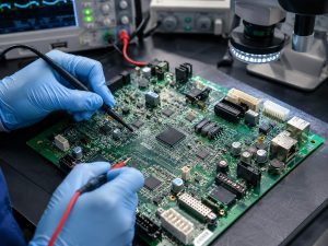
  3. ESD-safe insertion: Align pin 1, support the board, and insert the device or socket evenly.
  4. Solder-process control: Apply the component manufacturer’s temperature and time limits. Tune wave, selective, or hand soldering to the board thermal mass.
  5. Cleaning: Confirm that the component, socket, markings, and seal are compatible with the cleaning chemistry and process.
  6. Post-solder inspection: Inspect fill, wetting, bridging, insufficient solder, lifted lands, contamination, lead damage, body cracks, and orientation.
  7. Electrical verification: Perform the required continuity, programming, functional, or system test after visual acceptance.
Gloved operator handling a dark ceramic DIP-16 package with ceramic-tip tweezers on an ESD-safe work surface

A socket can reduce heat exposure and simplify replacement, but it adds contact resistance, height, cost, and another mechanical interface. Direct soldering removes the socket interface but makes replacement and rework more difficult. Select the method from serviceability, vibration, reliability, and lifecycle requirements.

What Common Failures Should Designers and Buyers Prevent?

The most preventable failures come from wrong footprints, forced leads, incorrect orientation, unsupported substitutions, poor storage, and uncontrolled soldering. Ceramic construction does not compensate for a mismatched assembly process.

Failure Mode Likely Cause Prevention
Lead bending or package stress Incorrect row spacing or forced insertion Verify the drawing, use a fit check, and control lead forming
Wrong circuit behavior Pin-1 orientation or pinout error Align schematic, footprint, silkscreen, assembly drawing, and inspection program
Weak or open solder joint Wrong hole size, oxidized finish, insufficient heat, or poor flux access Control finished holes, storage, solder profile, and joint inspection
Body or seal damage Mechanical impact, clamping force, thermal shock, or aggressive rework Use protected handling, supported insertion, and approved temperature limits
Field reliability mismatch Assuming ceramic equals qualified or hermetic Require the exact device grade, test evidence, and approved source
Early redesign or shortage Obsolescence or single-source package dependency Check lifecycle status and qualify alternatives before production need becomes urgent

What Information Should Buyers Include in a DIP-16 RFQ?

A useful RFQ identifies both the component and the board-assembly requirements. “DIP-16 ceramic” alone leaves too many variables open and can lead to an electrically correct but mechanically or commercially unsuitable substitution.

  • Manufacturer and complete component part number.
  • Package designator and controlled mechanical drawing revision.
  • Required temperature grade, qualification, screening, and traceability.
  • Lead material and finish, including any solderability or gold-removal requirement.
  • Approved alternates and the engineering change process for substitutions.
  • Gerber or ODB++ data, drill files, fabrication drawing, assembly drawing, BOM, and centroid data where applicable.
  • Direct solder or socket requirement, board quantity, prototype and production volumes, and test scope.
  • Packaging, storage, date-code, shelf-life, and counterfeit-avoidance requirements.

If the component is obsolete or allocation-sensitive, ask for source traceability and do not authorize an alternate based only on the words “DIP-16.” Pinout, speed grade, temperature range, package seal, finish, dimensions, and qualification must all be reviewed.

FAQ About DIP-16 Ceramic Packages

1. Is every DIP-16 ceramic package hermetic?

No. Ceramic describes the package material or construction, while hermeticity is a verified package performance requirement. Confirm the seal type, package specification, leak-test requirement, and device documentation.

2. What Is a Dual In Line Package, and Does Every DIP-16 Use a 2.54 mm Lead Pitch?

A 2.54 mm pitch is common for standard dual in-line packages, but the approved mechanical drawing remains the authority. Do not release a footprint from the package name alone.

3. Can a ceramic DIP-16 replace a plastic PDIP-16?

Only after engineering verifies pinout, electrical ratings, timing, temperature range, body and lead dimensions, finish, qualification, and system requirements. A shared pin count does not make two devices equivalent.

4. Should a ceramic DIP-16 be socketed or soldered directly?

Use a socket when replacement, programming, or thermal isolation during assembly is important. Direct soldering may be preferable when contact interfaces, height, vibration, or cost are more critical. Evaluate the complete operating environment.

5. How is the correct plated-hole diameter selected?

Start with the maximum lead cross-section, then add insertion allowance and account for plating and drill tolerances. The PCB fabricator and assembler should review the finished-hole requirement together.

6. What should be inspected after soldering?

Check orientation, body and seal condition, lead damage, solder wetting, hole fill, bridging, contamination, lifted pads, and board damage. Complete the electrical or functional test required by the product plan.

How Can EBest Circuit Support a DIP-16 PCB Assembly?

A reliable DIP-16 assembly starts with the correct component drawing, plated-hole design, solder method, inspection criteria, and substitution controls. At EBest Circuit, we can review your PCB fabrication and PCBA package for through-hole or mixed-technology production. Send us the Gerber files, drill data, BOM, assembly drawing, package drawing, quantities, and test requirements so our engineering team can evaluate manufacturability and prepare a quotation at sales@bestpcbs.com.
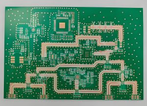
You may also like

Modular PCB Design for Scalable Multi-Board Systems

August 25th, 2026

modular PCB design divides an electronic system into defined functional boards or circuit blocks that can be developed, verified, replaced, and reused with controlled interfaces. It is useful when a product family needs several configurations, when different teams work in parallel, or when one subsystem is likely to change before the rest of the product.

The method does not make a system reliable by itself. A module boundary adds connectors, return-path transitions, power-entry conditions, mechanical tolerances, and version-control decisions. The design succeeds only when those interfaces are treated as engineering specifications rather than convenient pin headers added near the end of layout.

Modular PCB Design with a main board and interchangeable functional PCB modules

What Is Modular PCB Design?

Modular PCB design is a system architecture in which each module has a defined function, a controlled interface, and a clear verification boundary. A module might handle power conversion, processing, sensing, motor control, communication, data acquisition, or a user interface.

Modularity can exist at two levels:

  • Logical modularity: functional blocks remain on one PCB but use separate schematic sheets, layout zones, power domains, and test boundaries.
  • Physical modularity: functions are placed on separate boards connected by mezzanine connectors, card-edge contacts, cables, backplanes, or soldered modules.

A product does not need multiple boards to benefit from modular thinking. Even a single-board design becomes easier to review when power, analog, digital, RF, and safety-related sections have explicit boundaries. Physical separation is justified when it improves reuse, serviceability, configuration control, parallel development, enclosure fit, or risk isolation enough to offset the added interconnect cost.

Which Modular PCB Architecture Fits the System?

The best architecture follows the product’s service model, signal bandwidth, available volume, mechanical envelope, and expected upgrade path. It should not be chosen only because stacked boards look compact.

Architecture Best Fit Main Constraint
Motherboard with daughtercards Products with optional or replaceable functions Connector alignment, stack height, and local support
Backplane with plug-in cards Expandable industrial, communications, and test systems Shared power, bus loading, card guides, and airflow
Stacked boards Compact embedded devices with limited footprint Thermal shadowing, inspection access, and tolerance stack
Cable-linked boards Modules placed around an enclosure or moving assembly Cable loss, EMI, strain relief, and connector retention
Soldered castellated module Reusable RF, sensing, or processing subassemblies Reflow profile, pad geometry, rework, and test access

For a deeper look at stacked structures and their assembly implications, compare this architecture decision with our PCB on PCB design guide. That physical stacking decision is only one part of a complete modular system.

Comparison of motherboard daughtercards, backplane plug-in cards, and stacked PCB architectures

How Should Functional Boundaries Be Defined?

Start with functions and failure domains, not arbitrary board outlines. A useful boundary minimizes the number of signals crossing between modules while keeping each module independently understandable and testable.

Review each proposed boundary against these questions:

  • Does the module perform one coherent function with clear inputs and outputs?
  • Can it be powered, programmed, and tested without the complete product?
  • Are high-current paths, precision analog signals, clocks, RF feeds, or safety barriers being forced through an unnecessary connector?
  • Will the module be reused across enough products or variants to justify interface control and separate lifecycle management?
  • Can a failed module be isolated without replacing a large portion of the system?

Create an interface control document before detailed layout. It should identify every pin, direction, electrical level, power state, allowable load, timing requirement, reference ground, pull-up ownership, default state, reserved position, mating sequence, and compatibility rule. The document should also state which module revision is compatible with each host-board revision.

Module interface definition separating power, ground, high-speed data, control, and reserved contacts

How Should a Modular PCB Connector Be Specified?

A modular PCB connector must be selected as an electrical, mechanical, assembly, and service component at the same time. Pitch and pin count alone are not enough.

  • Electrical: current per contact, contact resistance, voltage rating, ground-to-signal ratio, shielding, and high-speed performance.
  • Mechanical: mating height, insertion force, retention, alignment features, durability cycles, keying, and tolerance to vibration or shock.
  • Assembly: SMT or through-hole termination, coplanarity, reflow compatibility, paste design, inspection access, and repair method.
  • Lifecycle: availability, second-source strategy, connector revision control, and the consequence of obsolescence.

Place ground contacts beside sensitive or fast signals when the connector system supports it. Avoid assigning every ground pin to one end of a long connector because that can force return current to take a larger loop. For removable modules, add polarization or mechanical keying so an incompatible card cannot be inserted in the wrong orientation.

How Do Signal Integrity and Return Paths Cross Module Boundaries?

Every connector is an impedance discontinuity. The signal sees PCB traces, pads, vias, contacts, another set of pads and vias, then a second PCB. At low edge rates this transition may be forgiving; at high edge rates it can create reflection, loss, crosstalk, mode conversion, and timing error.

Control the complete channel rather than checking each board in isolation:

  • Route fast signals over continuous reference planes up to the connector launch.
  • Provide nearby ground contacts so return current can cross the same physical boundary.
  • Minimize stubs, unused connector branches, and unnecessary layer changes.
  • Keep differential pair geometry and skew controlled through both launches.
  • Include connector models, via models, and both PCB stackups in channel simulation when the data rate requires it.
  • Define whether termination is located on the source module, destination module, or backplane.

Our high-speed digital PCB guide explains controlled impedance, differential pairs, vias, crosstalk, and return-path planning in more detail.

Signal integrity and power integrity controls across a board-to-board module boundary

How Should Power Be Distributed Across Modular Circuit Boards?

Power architecture should be defined before connector pinout. Decide whether the host distributes raw input power, regulated system rails, or both. A raw-bus approach gives each module local regulation and fault isolation, while shared regulated rails can reduce duplicate circuitry but make voltage drop, transient loading, and compatibility more sensitive.

For every rail crossing modular circuit boards, document:

  • Nominal voltage, tolerance, continuous current, peak current, and startup current.
  • Contact allocation, current derating, acceptable voltage drop, and temperature rise.
  • Power-up and power-down sequence, reset behavior, and back-powering risks through signal pins.
  • Local input capacitance, decoupling, bulk storage, and load-transient limits.
  • Fuse, current-limit, reverse-polarity, overvoltage, and fault-containment strategy.
  • Whether live insertion is prohibited or intentionally supported.

Do not assume a removable card is hot-swappable. Live insertion may require staggered contacts, pre-charge, inrush control, power-good logic, and firmware behavior that prevents undefined bus activity. If the product is serviced only when powered off, say so clearly in the interface and service documentation.

Which Mechanical and Thermal Constraints Need Early Control?

A modular electrical design can fail at integration because the boards do not mate reliably, the enclosure loads the connector, or one card blocks airflow to another. Use the mechanical model early enough to influence board outline and placement.

  • Set connector location, mating height, board spacing, and allowable positional tolerance as shared dimensions.
  • Add guide pins, card guides, standoffs, screws, latches, or enclosure features when the connector should not carry the full mechanical load.
  • Check keep-outs around extraction paths, fasteners, cable bends, test probes, and rework tools.
  • Model component height on both sides of every board, including manufacturing tolerances.
  • Review heat-source alignment, airflow blockage, heatsink access, and thermal coupling between stacked modules.
  • Define the expected insertion cycles and service environment before choosing a connector family.

Mechanical reference points must match across the PCB outline, assembly drawing, enclosure model, and connector drawing. Small coordinate or revision errors can create a system-level interference even when each individual board passes inspection.

How Should Each Modular PCB Board Be Prepared for Manufacturing?

Each modular PCB board needs its own buildable data package plus one system-level document that connects the revisions. Reusing a circuit block does not mean reusing an old manufacturing package without checking its current components, stackup, footprint data, and interface revision.

Before release, apply the same fabrication and assembly discipline to every module:

  • Gerber or approved intelligent data, NC drill files, board outline, and fabrication drawing.
  • Stackup, controlled-impedance requirements, material, copper, finish, thickness, and tolerances.
  • BOM, centroid data, assembly drawing, polarity notes, approved substitutions, and do-not-fit variants.
  • Connector part numbers, mating orientation, stack height, keep-outs, and inspection requirements.
  • Programming files, module serial or revision marking, test procedure, and pass/fail limits.

Run a PCB design for manufacturability review on each board and then repeat the review at the system level. The second pass catches problems that a board-only check misses, such as inaccessible connectors, blocked test points, conflicting revisions, and assembly-order constraints.

How Should a Modular PCB System Be Tested?

A modular PCB system should be verified in layers: module test, interface integration test, and complete system test. Passing a module-level functional test does not prove that the connector channel, shared power network, firmware handshake, enclosure, or thermal environment will work after integration.

  1. Test each module independently. Verify its power input, outputs, communications, programming, protection, and boundary conditions.
  2. Use known-good counterparts. A golden host board or golden module helps isolate whether a failure follows the module or the interface.
  3. Test every interface state. Include startup, reset, sleep, communication loss, overload, missing module, incorrect revision, and permitted insertion or removal conditions.
  4. Validate the complete assembly. Measure signal margins, rail behavior, temperatures, EMI-sensitive conditions, and performance inside the final enclosure.
  5. Preserve traceability. Record board revision, firmware version, BOM variant, module serial number, and test result as one system configuration.

Test points should remain accessible before and after modules are installed. If a fixture cannot contact critical nets in the assembled state, provide a dedicated test connector, boundary-scan path, built-in self-test, or another agreed diagnostic interface.

Module test, integration test, and complete modular PCB system test workflow

When Does a Modular Design Add Cost or Risk?

Modularity is not automatically cheaper. It can reduce redesign and service cost while increasing unit hardware cost. The correct comparison uses total product and lifecycle impact, not the PCB price alone.

Potential Benefit Possible Added Cost or Risk
Reuse of validated functions Interface documentation and compatibility validation
Parallel development More coordination, revision control, and integration testing
Replaceable or upgradeable modules Connectors, retention hardware, enclosure volume, and service access
Fault isolation Extra protection, diagnostic circuitry, and test fixtures
Product configuration from common blocks Variant management, inventory, and end-of-life coordination

A monolithic board may be better when the product is small, cost-sensitive, built in one stable configuration, and dominated by short high-speed or high-current paths. A modular architecture becomes stronger when the product family changes frequently, field replacement matters, teams can truly work in parallel, or validated functions will be reused across several products.

FAQ About Modular PCB Design

  • Is a modular PCB the same as a daughterboard? No. A daughterboard is one physical module type. Modular design also includes backplanes, stacked boards, cable-linked assemblies, soldered modules, and logical blocks on one PCB.
  • Can a modular PCB improve repairability? Yes, when failed functions can be diagnosed and replaced independently. Repairability still depends on accessible connectors, spare-module control, service documentation, and safe replacement procedures.
  • Are board-to-board connectors suitable for high-speed signals? They can be, but the connector, launches, vias, reference contacts, stackups, and complete channel must meet the interface bandwidth and signal-integrity requirements.
  • Should every module use the same connector? Not necessarily. Standardization helps reuse, but power, high-speed, RF, safety, mechanical, and environmental requirements may justify different connector families.
  • What files are needed to quote a multi-board assembly? Provide the fabrication package for every PCB, BOM and placement data for every assembly, mechanical drawings, the module/interface definition, test requirements, quantities, variants, and one revision matrix for the full system.

The most important rule is to treat modular PCB design as a controlled system architecture. Reusable boards are valuable only when their electrical, mechanical, firmware, manufacturing, and test interfaces remain explicit.

How Can EBest Circuit Support Your Modular PCB Project?

At EBest Circuit, we support PCB fabrication, component sourcing, PCBA assembly, DFM review, and agreed inspection or functional testing for multi-board electronic products. We can review the individual module files together with connector orientation, stack height, controlled-impedance needs, assembly sequence, and system test access before the build is released.

For a useful engineering review and quotation, send the Gerber or ODB++ data for each board, NC drill files, stackups, fabrication drawings, BOMs, placement files, assembly drawings, connector specifications, quantities, revision matrix, and test requirements. Our PCB manufacturing and assembly guide can help you organize that package.

Email sales@bestpcbs.com with your project files and system constraints. We will review the manufacturing and assembly scope against the actual module architecture instead of treating each PCB as an unrelated order.

You may also like

BT Substrate Guide: Material, Process, Applications and ABF Comparison

August 25th, 2026

A BT substrate is an organic semiconductor package substrate built with bismaleimide triazine resin laminate. It provides the fine copper interconnection layer between a silicon die and the larger system PCB, especially in BGA, CSP, memory, RF, and other compact packages.

The material name alone does not define performance. Resin grade, reinforcement, copper profile, layer structure, microvia design, finished thickness, surface finish, and package assembly all affect electrical behavior, warpage, and reliability. This guide separates those decisions so engineers and buyers can specify the substrate without treating BT as a universal recipe.

BT Substrate cutaway showing an IC die, copper routing layers, laminate core, microvias, solder balls, and system PCB

What Is a BT Substrate?

A BT substrate is a fabricated organic package substrate whose insulating structure uses bismaleimide triazine resin material.

It sits inside the semiconductor package. The die connects to fine copper features on the top side by wire bonds or flip-chip bumps, while pads or solder balls on the bottom side connect the package to the system board. In other words, the substrate redistributes a very fine die interface into a larger, manufacturable package interface.

Three terms are often mixed together. BT resin is the thermoset chemistry. BT laminate is the cured, reinforced material supplied in sheet or prepreg form. The finished BT resin substrate adds copper circuits, vias, solder mask, surface finish, and dimensional controls for a specific package. It is not simply another name for the motherboard beneath the package.

BT Substrate Material: Resin, Reinforcement, and Copper Structure

BT substrate material normally combines a thermoset BT resin system, reinforcement or fillers, and patterned copper conductors.

The exact formulation is supplier- and grade-specific. A datasheet may report glass-transition behavior, dielectric constant, dissipation factor, coefficient of thermal expansion, moisture absorption, peel strength, and dimensional change. Those values must be compared at the stated frequency, thickness, cure condition, and test method; numbers taken from different grades are not automatically interchangeable.

BT Substrate Material exploded view with copper routing, BT resin core, build-up dielectric, microvias, and solder mask
  • BT resin core or prepreg: provides insulation, structural support, and thermal stability.
  • Reinforcement and fillers: influence stiffness, dimensional control, drilling behavior, and thermal expansion.
  • Copper foil or plated copper: forms signal, power, ground, pads, and vertical interconnections.
  • Microvias and through connections: link routing layers according to the package architecture.
  • Solder mask and surface finish: protect conductors and prepare pads for wire bonding, bumps, or solder balls.
Do not approve a material only because the datasheet says “BT.” Approve the exact grade, construction, copper type, thickness, and qualification evidence used for the package.

Why Is BT Resin Used in IC Package Substrates?

BT resin is used because it combines useful thermal, electrical, and mechanical behavior with scalable organic-laminate processing.

Mitsubishi Gas Chemical identifies its BT laminate as a thermoset bismaleimide triazine material developed for chip packaging, with particular emphasis on thermal resistance, electrical properties, structural integrity, and low warpage. The IEEE IRDS packaging tutorial also identifies BT resin as an organic substrate material widely used for BGA and CSP packages.

These strengths matter because a package substrate experiences several stresses at once: fine copper features must stay registered, the package must remain flat through repeated heating and cooling, and the dielectric must preserve insulation and signal behavior. BT is therefore attractive when a conventional low-cost board laminate does not provide enough package-level control, but the design does not require the finest ABF build-up architecture.

BT Substrate vs ABF Substrate

BT and ABF are both organic package-substrate material systems, but they are usually selected for different layer functions and routing densities.

BT commonly appears as a reinforced laminate and is strongly associated with wire-bond BGA, CSP, memory, MEMS, RF, and other mainstream packages. ABF is an unreinforced build-up dielectric designed for fine laser microvias and dense redistribution in advanced flip-chip packages. A complex substrate may use a core material and separate build-up films, so the decision is not always a simple one-material-versus-the-other choice.

BT Substrate vs ABF Substrate comparison showing wire-bond BGA and high-density flip-chip package structures
Comparison BT substrate ABF substrate FR-4 PCB
Primary role Organic IC package substrate High-density package build-up structure System-level printed circuit board
Typical structure Reinforced BT laminate with copper circuits and vias Thin build-up dielectric layers with dense laser microvias Glass-reinforced epoxy laminate with PCB-scale circuitry
Common fit BGA, CSP, memory, RF, MEMS, and related packages High-I/O flip-chip, CPU, GPU, ASIC, and advanced computing packages Board-level interconnection for packaged components
Selection trigger Package reliability and moderate-to-high routing density Very fine routing, high I/O count, and multilayer build-up needs Cost-effective board-level routing within PCB design rules

Choose from the package architecture outward. Die pad pitch, I/O count, escape routing, electrical model, substrate size, warpage target, assembly method, and reliability plan should drive the material system. A broad label such as “high performance” is not enough to select between BT and ABF.

How Does a BT Substrate Differ from an FR-4 PCB?

A BT substrate works at the semiconductor-package level, while an FR-4 PCB connects completed packages and other components at the system level.

The two products may share patterning, drilling, plating, lamination, and inspection concepts, yet the tolerances and interfaces are different. A package substrate must handle die attachment, wire bonding or flip-chip connections, fine redistribution, solder-ball interfaces, and package warpage. A conventional PCB is designed around component land patterns, board stackup, assembly, connectors, and system-level mechanical constraints.

When board-level density becomes difficult but a true package substrate is not required, a substrate-like PCB or advanced HDI PCB may be the correct middle ground. The functional boundary should be settled before requesting minimum line or via dimensions.

BT Substrate Process: How Is It Manufactured?

The BT substrate process builds a controlled multilayer interconnect through material preparation, circuit formation, via creation, copper deposition, lamination, finishing, and inspection.

The route changes with the layer count, conductor-formation method, via architecture, and package type. A representative sequence is:

  1. Material preparation: condition and prepare the specified BT laminate, prepreg, copper, and build-up materials.
  2. Inner circuit formation: coat, expose, develop, and etch or plate the required copper pattern.
  3. Via formation: create mechanical holes or laser microvias, then desmear and prepare the walls.
  4. Metallization: deposit and plate copper to connect the layers and form the conductor thickness.
  5. Layer build-up: align and laminate the multilayer construction; repeat build-up cycles when required.
  6. Outer-layer definition: complete fine routing, pad structures, solder mask, and the specified surface finish.
  7. Profiling and inspection: route or punch the unit and verify electrical, optical, dimensional, and structural requirements.
BT Substrate Process from material preparation and circuit patterning through microvias, copper plating, layer build-up, inspection and test

Process capability cannot be inferred from the resin name. Fine-line geometry, copper adhesion, microvia aspect ratio, layer registration, panel handling, and yield must be reviewed as one construction. The manufacturing data should therefore identify the exact stackup and finished geometry, not only “BT material.”

Which Package Types and Applications Use BT Substrates?

BT substrates are widely used where an organic package needs stable fine routing, compact form, and dependable thermal-cycle behavior.

  • Wire-bond BGA and CSP: redistributes die connections to an area-array package interface.
  • Memory packages: supports compact routing and thin package structures.
  • MEMS and sensor packages: provides controlled mechanical and electrical interconnection around sensitive devices.
  • RF and communication packages: uses grade-specific dielectric behavior and controlled geometry for signal paths.
  • LED and optoelectronic packages: supports compact package routing, although thermal architecture must be assessed separately.
  • Multi-chip and system-in-package designs: can connect several dies or functions when the selected substrate architecture supports the required density.

These are application families, not automatic material approvals. High-power, very-high-frequency, large-body, or ultra-fine-pitch packages may require ABF, ceramic, glass, metal, or another specialized substrate. Use package simulation and reliability targets to confirm the choice.

Which Design Inputs Matter Most for a BT Substrate?

The most important inputs are the complete package interconnect, stackup, material, mechanical, assembly, and test requirements.

  • Die size, pad map, pad metallurgy, and wire-bond or flip-chip interface.
  • Package outline, substrate thickness, cavity or stiffener needs, and flatness or warpage limits.
  • Layer count, copper thickness, line/space, impedance targets, reference planes, and current paths.
  • Via type, drill or laser diameter, capture pad, filling requirement, stacking rule, and reliability target.
  • Exact BT material grade, copper type, solder mask, surface finish, and approved alternatives.
  • Bottom-side pad or solder-ball layout, pitch, coplanarity, and downstream assembly profile.
  • Panel format, unit orientation, fiducials, coupons, inspection criteria, quantity, and qualification lot plan.

Start with a package drawing and netlist, then align the design database and fabrication notes. If the request only includes a PDF picture and the phrase “BT substrate,” the supplier cannot reliably price or validate the construction.

What Reliability Risks Need Control?

The main risks are warpage, dimensional shift, layer misregistration, via failure, copper adhesion loss, moisture-related damage, and incompatible assembly interfaces.

Risk Why it matters Control focus
Warpage Disturbs die attach, wire bonding, bump contact, or solder-ball coplanarity Balanced construction, material behavior, copper distribution, cure and thickness control
Registration error Reduces pad capture and may create opens or shorts Artwork compensation, alignment strategy, tooling and in-process measurement
Microvia or plated-via failure Breaks vertical interconnection during assembly or thermal cycling Geometry, cleaning, plating quality, fill condition and structural inspection
Copper adhesion loss Can produce lifted pads or delamination Surface preparation, compatible materials, cure control and peel/reliability evidence
Moisture damage Raises delamination and package-cracking risk during reflow Material handling, bake/dry controls, packaging and assembly exposure management

The risk list should become a control plan, not a generic warning. Define measurable acceptance criteria, sampling, coupons, and qualification conditions before production so the inspection method matches the failure mechanism.

How Should a BT Substrate Be Inspected and Qualified?

Qualification should combine electrical, optical, dimensional, structural, and package-level reliability evidence.

Typical checks include automated optical inspection of fine conductors, electrical continuity and isolation testing, dimensional and warpage measurement, copper-thickness verification, microsection analysis, surface-finish inspection, and X-ray or other structural methods where the construction requires them. The final plan depends on package risk and cannot be replaced by one certificate.

Before approving a supplier, compare the drawing revision, material certificate, stackup, process route, inspection report, coupon results, and change-control method. If the package will be wire bonded, flip chipped, molded, or soldered through a demanding reflow cycle, include assembly-side validation rather than accepting the bare substrate alone.

FAQ About BT Substrates

What does BT stand for in substrate material?
BT stands for bismaleimide triazine, the thermoset resin family used in the laminate. The finished substrate also contains copper conductors, vias, protective coatings, and a package-specific surface finish.
Is a BT substrate the same as an IC substrate?
BT substrate is one type of organic IC substrate. IC substrate is the broader product category and may use BT, ABF, epoxy, ceramic, glass, or other material systems depending on the package.
Can BT substrate material values be copied between suppliers?
No. Compare the exact grade and the stated test conditions. Frequency, specimen thickness, cure, copper treatment, reinforcement, and test method can change reported dielectric, thermal, and mechanical values.
Is BT always cheaper than ABF?
No universal price rule applies. Cost depends on material grade, layer structure, feature density, panel utilization, process yield, qualification, volume, and supply conditions. A simpler BT construction may be more economical, but it cannot replace ABF when the routing architecture requires fine build-up layers.
Can a BT substrate use microvias?
Yes, depending on the material construction and fabricator process. Microvia diameter, depth, capture pad, stacking, filling, and reliability requirements must be engineered together rather than copied from a conventional PCB rule set.
What files are needed for a BT substrate review?
Provide the package drawing, layer data or Gerber/ODB++ package, netlist, drill and microvia details, material grade, stackup, pad finish, mechanical tolerances, assembly interface, reliability requirements, quantity, and revision status.

How Can EBest Circuit Support Your BT Substrate and PCB Project?

At EBest Circuit, we support IC substrate, advanced PCB, component sourcing, and PCBA projects from engineering review through production planning.

For a BT package project, we first separate package-substrate requirements from system-board requirements, then review the material, stackup, conductor geometry, vias, finish, inspection plan, assembly interface, quantity, and qualification needs. Our broader IC substrate guide can help your team confirm the correct product category before quotation.
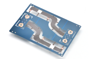
Send your package drawing, fabrication data, stackup, material grade, surface finish, quantity, and reliability requirements to sales@bestpcbs.com. We will review the data, identify items that need engineering confirmation, and help establish a practical substrate-to-PCB production route. You can also return to this BT substrate guide when aligning the package and system-board specifications.

You may also like

Dot PCB Guide: Meaning, Pad Layout, Soldering and Design Limits

August 25th, 2026

A Dot PCB is a solderable prototyping board with a regular hole grid and an individual copper pad around each hole. Unlike stripboard, neighboring holes are normally not connected, so the builder creates every electrical node with component leads, jumper wire or carefully controlled solder links. It is useful for simple through-hole prototypes, but it does not provide the repeatability, routing control or production readiness of a custom PCB.

This guide focuses on the details that determine whether a dot board works reliably: pad pattern, component-side versus copper-side orientation, node planning, soldering, inspection and the point at which manual wiring should become a manufactured circuit board.

Dot PCB with isolated copper pads and through-hole electronic components

What Is a Dot PCB?

A Dot PCB is a general-purpose perfboard used to build soldered electronic prototypes without designing a custom copper pattern first. Each hole acts as a mechanical mounting point, while its surrounding copper pad provides a solderable land for a component lead or wire.

The board is most suitable for small, low-speed, through-hole circuits such as LED indicators, sensor interfaces, simple timers, relay drivers and microcontroller support circuits. It is less suitable when current, noise, frequency, geometry or repeatability must be tightly controlled.

Dot PCB Full Form and Common Names

The search phrase dot pcb full form does not expand into a separate formal engineering term. The word Dot describes the visible grid of isolated copper dots, while PCB means printed circuit board. Depending on the market, the same or a closely related product may be sold as:

  • Dot board or dotted PCB
  • Pad-per-hole perfboard
  • Zero PCB
  • Universal prototyping board
  • Solderable protoboard

These names are not always interchangeable. A stripboard has continuous copper tracks, while a breadboard-pattern solder board copies the hidden connection groups of a solderless breadboard. Check the copper side instead of relying only on the product name.

How Does a Dot PCB Board Connect Components?

A dot pcb board does not create a circuit merely by holding parts. Every electrical connection must be deliberately formed between isolated pads. Common methods include insulated jumper wire, tinned solid wire, bent component leads and short solder bridges used only where spacing and inspection remain manageable.

Close view of isolated copper pads and through-hole leads in a Dot PCB

Plan each net as a group of points that must be electrically common. Power and ground paths deserve special attention because a long chain of small solder links can be difficult to inspect and may not suit the required current. Use wire of an appropriate gauge, provide mechanical support at connectors and keep sensitive signal paths away from switching or high-current wiring.

Which Materials and Pad Patterns Are Common?

Dot boards are commonly sold in paper-phenolic and fiberglass-reinforced laminate versions, with copper pads on one side or both sides. Product listings often use a 2.54 mm grid because it matches many through-hole IC sockets, headers and discrete components, but the actual pitch, hole diameter and pad size must be checked before purchase.

Board feature What to verify Why it matters
Base material Phenolic or fiberglass laminate Changes stiffness, heat tolerance and durability during rework
Copper pattern Isolated pads, strips or breadboard-style groups Determines which holes are already connected
Copper sides Single-sided or double-sided Affects access, anchoring and routing options
Pitch and hole size Match component leads and headers Prevents forced insertion and poor mechanical support
Board dimensions Usable grid area and mounting holes Controls component spacing and enclosure fit

Dot PCB vs Stripboard vs Breadboard: What Changes?

The main difference is how the holes are electrically connected. A Dot PCB normally leaves every pad isolated, stripboard connects holes along copper strips, and a solderless breadboard uses reusable spring contacts arranged in hidden groups.

Dot PCB, stripboard and breadboard connection-pattern comparison
Board type Connection pattern Best use Main limitation
Dot PCB Individual copper pads Flexible soldered through-hole prototypes Every net must be wired manually
Stripboard Continuous copper strips Ordered layouts that follow row-based routing Tracks must be cut where isolation is required
Breadboard Reusable internal spring contacts Fast experiments and component-value changes Loose wiring and limited mechanical stability
Custom PCB Designed copper traces and planes Validation, repeatability and production Requires design files and fabrication

For a broader development-stage comparison, see our proto board guide. The important purchasing check is the underside pattern: product photos of the component side alone may not reveal whether pads are isolated or connected.

How Should You Plan a Dot PCB Layout Before Soldering?

Plan the layout from the schematic before installing parts. A hand-wired prototype becomes difficult to debug when component placement is improvised while soldering.

  1. Mark the board orientation. The copper-side view is mirrored relative to the component side. Choose one reference corner and keep it consistent.

  2. Place fixed mechanical items first. Position connectors, switches, displays, sockets and mounting holes before small passives.
  3. Group components by circuit block. Keep the input, power regulation, controller and output sections visually distinct.
  4. Map power and ground nodes. Decide wire gauge, return paths and connection points before adding signals.
  5. Keep decoupling components close. Place each required bypass capacitor near the device pins it supports.
  6. Reserve test access. Leave points for ground, supply rails and important signals.
  7. Check the mirrored plan. Compare the component-side sketch with the copper-side connections before soldering.

A photo or marked drawing of both sides becomes useful design evidence later. It helps convert the prototype into a schematic and then into a controlled PCB layout.

How Do You Perform Dotted PCB Soldering?

Dotted pcb soldering works best when each joint is completed as a controlled pad-and-lead connection, followed by a separate wiring step. Do not attempt to draw long tracks with oversized solder blobs.

Hand soldering an isolated pad on the underside of a Dot PCB
  1. Work on an unpowered board and secure it in a holder.
  2. Confirm component value, pinout and polarity before insertion.

  3. Touch the clean, tinned iron tip to the pad and lead together.
  4. Feed electronics solder into the heated joint, not directly onto the iron.
  5. Stop once solder has wetted both surfaces and formed a controlled fillet.
  6. Remove the solder, then the iron, and keep the joint still while it cools.
  7. Trim the lead only after inspection, without pulling against the pad.
  8. Add jumper wires one net at a time and check continuity as the build progresses.

Our detailed guide on how to solder a PCB circuit board covers tool selection, joint inspection, rework limits and electrical safety in more depth.

Which Tools and Materials Are Needed?

A small, controlled tool set is safer than improvising with an oversized iron and plumbing materials. Prepare:

  • A temperature-controlled soldering iron with a tip suited to the pad size
  • Electronics solder and compatible electronics flux
  • A stable PCB holder, safety glasses and fume extraction
  • Flush cutters, wire strippers and ESD-safe tweezers
  • Insulated solid-core wire and appropriately sized power wire
  • Magnification, a multimeter and a current-limited bench supply
  • Solder wick or a suitable desoldering tool for corrections

The correct iron setting depends on alloy, tip geometry, pad size, wire mass and board material. Follow the solder and component guidance, then use the lowest practical setting that produces prompt wetting without prolonged contact.

What Common Dot PCB Faults Should You Check?

The most common failures are unintended shorts, open connections, mirrored-layout mistakes and mechanically weak wiring. Inspect the board before power-up and again after every repair.

  • Solder bridge: adjacent isolated pads are connected unintentionally.
  • Cold or poorly wetted joint: solder sits on the surface without bonding to both pad and lead.
  • Wrong-side routing: a copper-side connection was placed incorrectly because the mirrored view was not considered.
  • Lifted pad: excessive heat or mechanical force separates copper from the laminate.
  • Unsupported wire: movement transfers stress directly to a small solder joint.
  • Polarity or pinout error: a diode, capacitor, transistor or IC was installed in the wrong orientation.
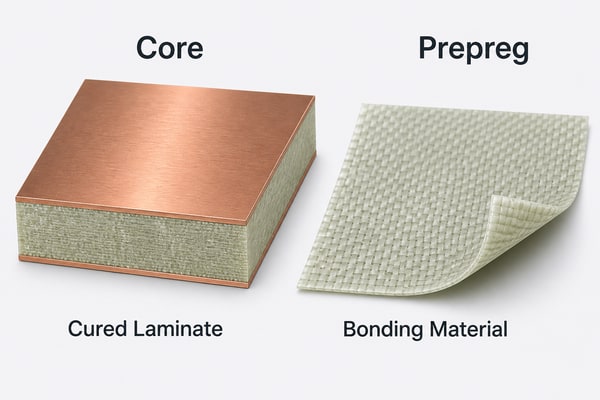
  • Hidden short under a component: clipped leads or bare wire touch where visual access is poor.

Check power-to-ground resistance, required continuity and unintended connections while the board is unpowered. Initial power-up should use an appropriate current limit when the circuit permits it.

When Is a Dot PCB Perfboard the Right Choice?

A dot pcb perfboard is the right choice when the circuit is small, uses accessible through-hole parts, operates at modest speed and power, and only one or a few hand-built units are needed.

It is particularly useful for educational builds, simple interface circuits, quick fixtures, one-off adapters and proof-of-concept hardware that needs stronger connections than a solderless breadboard. It also gives the designer freedom to arrange irregular through-hole parts without cutting stripboard tracks.

The choice becomes less attractive as wire count, assembly time, test requirements or unit quantity increase. A low board price does not compensate for hours of manual wiring and troubleshooting.

Which Circuits Should Not Stay on a Dot PCB?

A Dot PCB should not be treated as a production substitute when electrical or mechanical behavior depends on controlled geometry. Move to a custom PCB when the design involves:

  • High-speed digital interfaces or controlled-impedance signals
  • RF circuits, antennas or tightly controlled return paths
  • Precision analog signals vulnerable to leakage, coupling or ground error
  • High current, high voltage or significant thermal dissipation
  • Fine-pitch SMD, QFN, BGA or dense mixed-technology assembly
  • Defined creepage, clearance, enclosure or connector geometry
  • Repeated builds that must behave consistently
  • Formal inspection, traceability or product qualification

A manufactured blank circuit board provides designed copper features, solder mask, silkscreen, drill control and a specified surface finish. Those controls matter once the prototype becomes engineering validation hardware.

What Affects Dot PCB Board Price?

Dot pcb board price is usually influenced by laminate material, dimensions, copper on one or two sides, plating quality, hole count, mounting features, pad finish, supplied accessories, order quantity and local distribution costs.

Compare usable area and construction rather than the lowest listed price alone. A board that sheds pads during rework or does not fit the component pitch can cost more in lost time than the purchase-price difference. For a one-off learning circuit, a basic board may be enough. For a prototype that will be handled or tested repeatedly, fiberglass construction and better-supported holes may be worth considering.

FAQ About Dot PCB

Is every hole on a Dot PCB connected? No. On a typical pad-per-hole board, each copper pad is isolated. Always inspect the copper side or check continuity because some products use strips or breadboard-style groups.

Can a Dot PCB be reused? Components can sometimes be removed and pads reused, but repeated heating can damage the copper and laminate. It is not reusable in the same convenient sense as a solderless breadboard.

Can SMD components be mounted on a dot board? Standard 2.54 mm boards favor through-hole parts. Some larger SMD parts can use adapter boards, but fine-pitch packages need matching pads and better process control.

Are the component side and copper side oriented the same way? No. When the board is flipped, the copper-side view is mirrored. Mark a reference corner and verify pin numbering before making connections.

Should adjacent pads be joined with solder? A very short, intentional bridge may be practical, but long solder tracks are hard to control and inspect. Jumper wire is usually clearer for longer connections.

What files are needed to convert the prototype into a custom PCB? Start with a confirmed schematic, BOM, connector and mechanical requirements, photos or wiring records, and test expectations. Gerber and drill files are then produced from the completed PCB layout.

How Can We Move a Dot PCB Prototype into Production?

At EBest Circuit, we support the step from a working hand-wired prototype to a controlled PCB and PCBA build. Our team can review the schematic, board outline, component footprints, BOM, connector locations, test needs and manufacturing risks before fabrication.
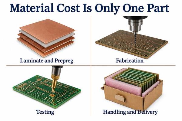
Before requesting a PCB prototype, capture every verified connection on the Dot PCB; do not rely on photos alone when wires overlap or disappear beneath components. Send your schematic, BOM, dimensions, quantity and available prototype records to sales@bestpcbs.com. We can help turn the verified circuit into fabrication files, assembled samples and a repeatable production path.

You may also like