Choosing a heavy copper PCB manufacturer in Europe takes more than comparing a maximum copper figure, a European office address, or a row of certification logos. A supplier that advertises 10 oz or 20 oz copper may still be unable to hold your required spacing, plate your hole structure, or reproduce the approved prototype in volume.
This guide shows you how to compare the complete construction, quality evidence, certification coverage, manufacturing location, lead time, and delivered cost on an equivalent basis. The supplier with the longest capability list or lowest unit price is not always the best fit; the stronger choice is the one that can prove your exact board is buildable, controlled, and deliverable on the terms your project needs.

What Should You Look for When Choosing a Heavy Copper PCB Manufacturer in Europe?
Start with the complete board construction and evidence from comparable production. These seven checks quickly separate a suitable factory from one relying on a maximum-copper figure or certification logos.
- Copper capability at your geometry. “Up to 10 oz” says nothing about the spacing the factory can hold at 10 oz. Your comparison needs the finished copper on each layer, the line width and spacing at that thickness, and any difference between inner- and outer-layer limits.
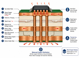
- Multilayer construction experience. A plant that makes a 6 oz double-sided board may not be able to build an eight-layer 6 oz stackup. Copper distribution, dielectric thickness, resin flow, lamination, overall thickness, and warpage all interact in a multilayer build.
- Hole and plating fit. Finished hole size, aspect ratio, annular ring, hole-wall copper, and via current duty belong in the same engineering conversation. Thick outer copper does not, by itself, prove adequate copper in the plated hole barrel.
- Evidence from a comparable job. A polished sample with a different layer count and copper weight has limited value. Microsections, copper measurements, electrical-test records, dimensional reports, and lot traceability are more useful when the previous build resembles your copper, geometry, and hole structure.
- Certificates tied to the factory. The document needs to cover the facility and activity involved in your order. A certificate held by a sales office, another group company, or an assembly plant does not automatically cover PCB fabrication.
- Continuity from prototype to production. Find out whether volume boards will use the same site, material, stackup, and approved process as the prototype. An attractive first build loses much of its value if production can move or change without notice.
- Real schedule and delivered cost. Factory days and unit price are only part of the decision. Engineering approval, material availability, inspection, transport, customs, freight, duties where applicable, and incoming handling can change which offer is genuinely faster or less expensive.
How Do You Compare Heavy Copper PCB Manufacturing Capabilities?
Compare copper thickness together with geometry, layer count, holes, material, and finishing. A maximum value taken from a capability chart cannot tell you whether the factory can manufacture the combination shown in your data.
Consider two suppliers. Supplier A promotes 10 oz copper but needs wider spacing at that thickness. Supplier B lists 6 oz as its practical limit and can hold your actual 6 oz traces, clearances, and finished holes. For a 6 oz design, Supplier B may be the closer technical match.
| Design Requirement | What to Compare | Why It Matters |
|---|---|---|
| Copper and geometry | Finished copper by layer with line width, spacing, and tolerance | Etching becomes less forgiving as copper gets thicker; a limit achieved on wide features may not apply to tighter geometry. |
| Layer count and distribution | Copper balance, dielectric thickness, resin fill, press cycles, and finished thickness | Uneven copper and high thermal mass can affect resin flow, dimensional stability, and warpage. |
| Holes and plating | Finished hole, aspect ratio, annular ring, barrel copper, and outer-layer buildup | Smaller holes become harder to plate and finish when the surrounding copper construction is demanding. |
| Solder mask and finish | Mask coverage, dams, clearances, application method, and surface finish | The raised conductor profile can challenge mask coverage and leave less room between adjacent features. |
| Material and temperature | Material properties, operating environment, thermal cycling, and copper expansion effects | A manufacturable board still needs a material system suited to its electrical, thermal, and reliability conditions. |
How Can You Verify a Manufacturer's Heavy Copper PCB Quality?
Use evidence that answers a specific risk in your board. Check what each record proves, how it was sampled, and whether it represents a comparable construction, rather than accepting a general claim that the factory performs inspection.
| Evidence | What It Can Show | Limitation |
|---|---|---|
| Microsection | Local layer copper, hole-wall plating, lamination condition, and visible voids | It examines selected locations; it does not describe every feature on every board. |
| Copper measurement | Whether sampled finished copper meets the stated target or minimum | Results are meaningful only when the method, location, tolerance, and sampling plan are known. |
| AOI record | Pattern inspection for conductor defects on the applicable layers | AOI does not replace electrical test or prove internal plating quality. |
| Electrical test | Continuity and isolation against the released net data | It does not establish copper thickness, dimensional accuracy, or long-term thermal reliability. |
| Dimensional report | Measured holes, outline, thickness, and drawing-controlled dimensions | Its value depends on the reported features, acceptance limits, and sampling level. |
| Lot traceability | Links among material batches, production lots, inspections, and shipped boards | A trace code is useful only if the underlying records are retained and retrievable. |
The copper result also needs a clear reference point: nominal or minimum, base or finished, inner or outer layer. These distinctions prevent a drawing requirement and a report value from sounding identical when they are not.
A well-made 4 oz sample does not prove capability for an eight-layer 8 oz board. Evidence from a similar copper weight, stackup, geometry, and hole structure gives a much stronger view of production readiness.
Which Certifications Matter for a Heavy Copper PCB Manufacturer in Europe?
- ISO 9001: Use it as a general quality-management baseline. The certificate should name the facility involved in your order and include relevant PCB manufacturing activities in its scope.
- IATF 16949, ISO 13485, or AS9100D: Match the certification to the end market and contract. Automotive, medical, and aerospace requirements are not interchangeable, and the quoted fabrication site must be covered.
- UL recognition: Check whether the applicable material system, product category, and construction are covered. A supplier logo alone does not establish that your quoted board falls within the recognition.
- RoHS and REACH: Treat these as product and material compliance requirements, not quality-management certificates. The declaration, material data, revision, and product coverage should match the board and destination market.
- Site, scope, and validity: The company name, address, certified activities, and expiry date must apply to the factory doing the work. A certificate for a sales office, another group site, or an assembly plant does not cover PCB fabrication automatically.
Does Your Heavy Copper PCB Need to Be Manufactured in Europe?
Not necessarily. Delivery to Europe and manufacturing in Europe are different requirements, and many projects can use an overseas factory when the technical, documentation, and supply-chain conditions are acceptable.
European fabrication may be required by a customer-approved source list, a contract, a controlled program, an internal sourcing policy, or a regional supply mandate. In that situation, the order documents should identify the permitted facility rather than relying on the supplier's registered address.
Overseas production may remain a practical option when there is no location restriction, the board fits the factory's processes, the quality records meet the project need, and the team can manage transport and import risk. Local sales or engineering support can be useful, but it does not change where fabrication takes place.
Choose the production region from the project constraint first. Then compare the actual plant, technical fit, production controls, delivery route, and total cost within the options that remain.
What Determines Heavy Copper PCB Lead Time in Europe?
There is no dependable standard lead time for heavy copper boards. The schedule changes with the copper weight, material availability, layer count, lamination cycles, plating demand, line and spacing, hole structure, test plan, quantity, and first-article needs.
The starting milestone can change the apparent result. One quote may count from purchase order receipt, another from completed engineering review, and a third from material availability or stackup approval. A five-day difference on paper may disappear once both schedules start at the same event.
Door-to-door time adds the steps outside fabrication: engineering questions, document approval, packing, transport, customs clearance where applicable, local delivery, and incoming inspection. A nearby factory may shorten logistics, while a well-planned overseas route may still fit a stable production schedule.
Compare dates only after the starting event, factory completion event, shipment method, destination, and approval assumptions are aligned.
Why Do Heavy Copper PCB Prices Vary So Much Between Manufacturers?
Two suppliers can quote the same “6 oz PCB” at very different prices because they may not be quoting the same build. One may be pricing 6 oz finished copper with tight spacing and a full inspection package; the other may be working from a different starting copper, stackup, or test assumption.
- Copper and process time: Heavy copper affects etching, plating, cycle time, process margin, panel utilization, and yield, not just the amount of raw copper.
- Geometry: A 6 oz layout with generous spacing does not carry the same manufacturing risk as 6 oz around tighter conductors and clearances.
- Layers and lamination: A double-sided power board and an eight-layer heavy copper build differ sharply in materials, press work, registration, and yield exposure.
- Testing and records: Microsections, dimensional reports, first-article inspection, special traceability, or customer-specific documentation add work that may or may not be included.
- Logistics: Freight, insurance, customs services, duties where applicable, local delivery, and incoming handling all affect the cost at the receiving dock.
For example, a €40 board quoted without freight, import charges, or extra inspection can cost more on arrival than a €46 board with a broader delivery and documentation package. Price becomes comparable only after the construction and included services are comparable.
What Should You Send Manufacturers to Get Comparable Quotes?
Send enough information for every factory to price the same board. Gerber files alone rarely settle the meaning of copper, material, tolerances, inspection, or delivery.
- Design files: Gerber or ODB++, drill data, fabrication drawing, netlist when available, and one clearly identified revision.
- Stackup: Layer count, board thickness, material or required properties, dielectric structure, and finished copper for each relevant layer.
- Critical geometry: Minimum line and spacing, finished holes, tolerances, annular-ring concerns, and required plated-hole copper where specified.
- Quality needs: Electrical test, microsection or cross-section needs, dimensional inspection, first-article records, traceability, and any customer-specific documents.
- Order details: Prototype and production quantities, expected lot sizes, delivery destination, target arrival date, and any fixed manufacturing-location condition.
If suppliers work from different technical assumptions, their prices cannot be compared fairly. Proposed material or stackup changes should appear clearly beside the offer, not emerge after the order is placed.
How Should You Compare Heavy Copper PCB Quotes?
Compare five items before looking at the final number: finished copper, stackup and material, inspection, lead-time definition, and delivery coverage. A difference in any one of them can create a price gap that has nothing to do with manufacturing efficiency.
| Quote Item | What Must Match | What Can Distort the Comparison |
|---|---|---|
| Finished copper | Layer-by-layer value, minimum or nominal requirement, and tolerance | Base copper presented as though it were the finished requirement |
| Stackup and material | Approved construction, overall thickness, and required material properties | An undisclosed equivalent, altered dielectric, or different press construction |
| Inspection | Test coverage, sampling, reports, and traceability deliverables | Special records priced separately or omitted |
| Lead time | Starting milestone, completion milestone, approvals, and quantity | Factory days compared with door-to-door time |
| Delivery | Destination, freight, customs responsibility, and other included charges | Different delivery terms or an incomplete landed-cost view |
The lowest number is not the lowest-cost equivalent build when the assumptions differ. Resolve the technical and delivery differences first; the remaining price comparison will be far more useful.
What Are the Most Common Mistakes When Choosing a Heavy Copper PCB Manufacturer?
Most poor selections begin with a shortcut: one impressive number, one attractive sample, or one low price is allowed to stand in for the complete build. Six mistakes deserve particular attention.
- Choosing by maximum copper thickness. The advertised limit may apply only to wider features or a simpler construction than yours.
- Mixing base copper and finished copper. The same “6 oz” description can lead to different process plans when the measurement point is not stated.
- Ignoring geometry at the target copper. Line width, spacing, holes, and annular rings can rule out a build even when the nominal copper is within range.
- Assuming a European office means European fabrication. Sales, engineering, warehousing, and board production may occur in different countries.
- Comparing unit prices built on different assumptions. Material substitutions, inspection exclusions, and delivery terms can make the cheapest line item the more expensive order.
- Approving a prototype without controlling later changes. A move to another plant, material, stackup, or process can break the link between the approved sample and the production board.
FAQs About Choosing a Heavy Copper PCB Manufacturer in Europe
Q1. How do I know whether a supplier's 10 oz capability applies to my design?
A1. Compare the 10 oz claim with your minimum line and spacing, finished holes, layer count, total board thickness, and material. Ask for a written DFM response tied to the current data revision, not a general capability chart.
Q2. Should finished copper be specified separately for inner and outer layers?
A2. Yes. Outer layers can gain copper during through-hole plating, while inner layers follow a different process route. State the finished requirement for each relevant layer and identify whether the value is nominal or minimum.
Q3. What evidence should I request before approving a heavy copper prototype?
A3. Ask for a microsection, copper-thickness results, electrical-test record, critical dimensional results, and lot traceability when those records matter to the design. The evidence should come from your build or a genuinely comparable construction.
Q4. Can the prototype and production order use different factories?
A4. They can, but the change needs explicit review and approval. If continuity matters, require the same build site, approved material, stackup, and process route, plus written notification before any production change.
Q5. Do PCBs delivered to Europe have to be manufactured in Europe?
A5. No, unless a contract, customer approval, program rule, or sourcing policy sets a location condition. Boards made elsewhere can be supplied to Europe when the technical, compliance, import, and delivery requirements are met.
Q6. When does the quoted heavy copper PCB lead time start?
A6. It depends on the supplier. The clock may start at purchase order receipt, engineering approval, stackup approval, or material availability, so the quotation should name the starting milestone and the promised completion or arrival event.
Q7. Why can two 6 oz heavy copper PCB quotes differ so much?
A7. The suppliers may be using different definitions for finished copper, geometry, stackup, material, inspection, yield allowance, freight, or import responsibility. Align those assumptions before treating the price gap as a true manufacturing-cost difference.
Q8. What should I send for an accurate heavy copper PCB quotation?
A8. Send Gerber or ODB++, drill data, fabrication drawing, stackup, finished copper by layer, critical line and spacing, finished holes and tolerances, material requirements, quantities, inspection needs, revision, and delivery destination.
Planning a heavy copper PCB for a European project? Send your design files, stackup, finished copper requirements, quantities, inspection needs, and delivery destination to sales@bestpcbs.com for a construction-specific quotation.