





An RFQ sent to several HDI PCB manufacturers in Germany can return offers based on very different production routes. One supplier may fabricate the board at a named German plant; another may handle engineering or prototypes in Germany and use capacity elsewhere in Europe or Asia for series production. The production site affects stackup approval, process ownership, delivery planning and the work required if the build later moves.
Decide first whether the program needs a German-built prototype, continuing German production or a planned move to an overseas series plant. Then give every candidate the same stackup, via map, materials, quantities and required ship date. That produces a fairer comparison of capability, lead time and total sourcing risk.

Compare 10 HDI PCB Manufacturers in Germany
German production is decisive for some projects; prototype speed, rigid-flex integration or a planned transfer to Asian volume may matter more for others. Compare these HDI PCB manufacturers in Germany by address, process limits, stated lead time and advantage to find the companies that fit the required production route.
| Manufacturer | German Address | HDI Process Capability | Lead Time | Advantages |
|---|---|---|---|---|
| KSG GmbH | Auerbacher Strasse 3–5 09390 Gornsdorf |
75 µm line/space; laser microvias, buried vias, stacked and staggered structures | 30 working days | Company-owned HDI production in Germany and Austria |
| CONTAG AG | Päwesiner Weg 30 13581 Berlin |
≤150 µm microvias and ≤100 µm structures; resin plugging and copper filling | 3 working days; from 14 hours | Very short prototype cycles from its Berlin plant |
| Unimicron Germany GmbH | Am Holländer See 70 47608 Geldern |
10-layer HDI example; filled and capped blind-via options | By quotation | German high-tech fab with access to group capacity in Asia |
| Würth Elektronik Circuit Board Technology | Salzstrasse 21 74676 Niedernhall |
MICROVIA.hdi, SLIM.hdi and ADVANCED.hdi; standard and custom buildups | From 2 working days | Strong design resources and standardized HDI technology families |
| Schweizer Electronic AG | Einsteinstrasse 10 78713 Schramberg |
Single, staggered, stacked and skipped microvias; hybrid HDI combinations | By quotation | HDI integration with automotive, RF and thermal technologies |
| Schaltungsdruck Storz | Carl-Benz-Strasse 1 79341 Kenzingen |
Up to 12 layers; 100 µm line/space and laser microvias ≥80 µm; more layers on request | By quotation | German manufacture with a managed partner route for selected series |
| ILFA GmbH | Lohweg 3 30559 Hannover |
50 µm laser-via example; blind, buried and stacked vias plus microfine structures | By quotation | Fine-feature engineering and in-house analytical capability |
| Kubatronik Leiterplatten GmbH | Karl-Benz-Strasse 13 73312 Geislingen/Steige |
75 µm line/space; blind, buried, stacked and staggered vias, via-in-pad and rigid-flex HDI | By quotation | HDI combined with flex and rigid-flex in German production |
| hmp HEIDENHAIN-MICROPRINT GmbH | Rhinstraße 134 12681 Berlin |
Up to 4+x+4; 75–150 µm laser blind holes, 75/75 µm line/space and microvia filling | By quotation | Specific published limits supported by broad in-house testing |
| Leiton GmbH | Wolframstrasse 96 12105 Berlin |
Structures to 75 µm; high-layer HDI exposure and German/Asian production routes | From 2 working days | German prototypes with managed transfer to China for series production |
KSG GmbH
KSG owns two HDI production sites: Gornsdorf in Germany and Gars am Kamp in Austria. Its published SBU capability includes 75 µm line/space, laser-drilled microvias, buried vias and stacked or staggered structures. Projects that require German origin should name Gornsdorf in the quotation; projects that permit either European site can also be considered for the Austrian plant.
The two-site model gives buyers a company-owned European alternative when German origin is not mandatory. If origin or qualification is controlled, the quotation should name the approved plant and state whether a move between Gornsdorf and Gars am Kamp would change the laminate, stackup, inspection plan or qualification record.
CONTAG AG
CONTAG’s Berlin plant is geared to short-cycle HDI prototyping. It publishes HDI/SBU production with microvias at or below 150 µm, conductor structures at or below 100 µm, resin plugging and in-house copper filling.
Standard service begins at three working days, while the multilayer Blitz service begins at 14 hours for eligible builds. Those lead times are most relevant during fast layout or test iterations. Express eligibility still depends on the via pairs, filling, materials and impedance targets in the proposed construction.
Unimicron Germany GmbH
Unimicron Germany pairs its Geldern high-tech plant with the wider group’s Asian capacity. The German operation publishes HDI production for samples, small and medium lots, and higher quantities; its documented work includes a 10-layer HDI example and filled or capped blind-via options.
The mixed footprint may suit a program that wants German development production and a possible group route to higher volume. The plants are not automatically interchangeable: the quotation should name the prototype and series sites and identify any change in laminate, buildup, panel format or test plan before the stackup is released.
Würth Elektronik Circuit Board Technology
Würth Elektronik publishes a detailed set of HDI planning resources. MICROVIA.hdi, SLIM.hdi and ADVANCED.hdi are supported by standard stackups, digital stackup files, design rules and impedance guidance.
Those resources are useful before the RFQ: a layout team can begin with a documented buildup and see where a custom impedance stackup is needed. Eligible online-shop boards are advertised from two working days, although the chosen HDI family and production site determine the actual route.
Schweizer Electronic AG
Schweizer combines microvia HDI with RF, thermal and automotive technologies. Its portfolio covers single, staggered, stacked and skipped microvias, along with buried and mechanically drilled connections.
Development and PCB production are both present at Schramberg. That combination is especially relevant for boards where dense digital escape is only one part of the job—for example, an RF section or a thermally demanding power area on the same PCB. The quoted buildup and production location define which parts of the wider technology portfolio apply.
Schaltungsdruck Storz
Storz combines in-house production in Kenzingen with qualified Asian partners for selected series work. Its German capability includes complex multilayers, HDI and microvia technology up to 12 layers, 100 µm line/space and laser microvias from 80 µm.
Storz also describes samples made under series conditions. This is useful when the first build must represent the later process rather than serve as a one-off demonstrator. Buyers can keep German production where origin or process control requires it, or evaluate the managed Asian route for suitable volumes.
ILFA GmbH
ILFA publishes a 50 µm laser-via example and discusses the registration challenge behind very small target pads. The Hannover manufacturer’s wider scope includes blind, buried and stacked vias, microfine structures and in-house laboratory analysis.
Its fine-via work and laboratory capability address tight BGA escape regions and stacked microvias, particularly when drilling-to-pad registration drives feasibility. The 50 µm figure is a documented example; usable dimensions still depend on the complete copper and dielectric construction.
Kubatronik Leiterplatten GmbH
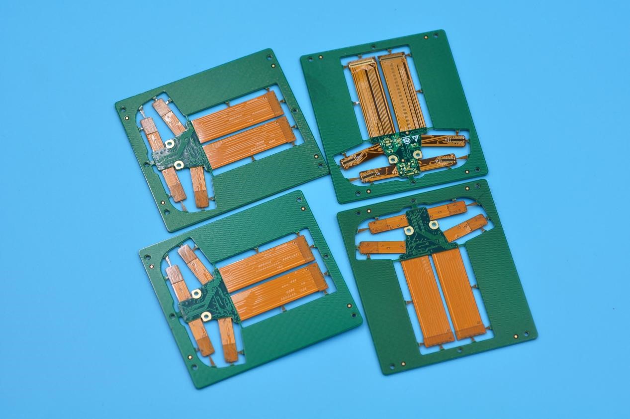
Kubatronik combines HDI/SBU with flex and rigid-flex manufacturing in Germany. Its published scope includes 75 µm line/space, blind, buried, stacked and staggered vias, via-in-pad and rigid-flex constructions with HDI layers. The company focuses on prototypes and low-to-medium volumes, addressing compact products that need dense component escape and a flexible interconnect in one construction.
For a rigid-flex HDI design, the complete construction needs one review rather than separate approvals for the dense rigid area and the flex tail. Microvia layer pairs, the rigid-to-flex transition, bend areas, coverlay openings and assembly clearances must work together; the published 75 µm line/space figure alone does not establish feasibility.
hmp HEIDENHAIN-MICROPRINT GmbH
hmp publishes concrete dimensions for its Berlin HDI process. The listed range covers SBU constructions up to 4+x+4, microvia filling, 75–150 µm laser-drilled blind holes and 75/75 µm line/space.
The published dimensions provide a starting range for an industrial board, supported by broad in-house testing. A design that approaches several limits at once still needs a complete stackup review because copper thickness, board thickness, material and via aspect ratio interact.
Leiton GmbH
Leiton links German prototype engineering with series production in China. Its Berlin headquarters handles inquiries, CAM preparation and technical clarification. Published services start at two working days, with 4–8-layer boards from three working days where the construction qualifies.
For a program that expects overseas volume, the series plant should review the stackup, blind-via arrangement and material family before the prototype layout is frozen. That review exposes geometry or material changes before the transfer becomes a second design cycle.
Comparison Criteria for German HDI PCB Manufacturers
Two quotations are comparable only when they describe the same board, production route and delivery point. Review each supplier against the following items before building a shortlist.
- Fabrication route: identify the plant for prototypes and the intended plant for repeat orders. Record any partner route, transfer point and country-of-origin restriction, then require approval before the named route changes.
- Accepted stackup and via map: submit the laser-via layer pairs, sequential-lamination cycles, buried vias, stacked or staggered connections and filled or capped via-in-pad requirements. The useful output is an approved buildup, not a general statement that HDI is available.
- Combined process window: obtain approval for line/space, laser-via diameter, capture pad, copper weight, dielectric thickness and finished board thickness together. Isolated published minima may not be available in one construction.
- Materials and impedance: agree the laminate family, copper, dielectric thicknesses, impedance targets, tolerances and coupon plan. List permitted equivalents and define which substitutions require customer approval.
- Prototype-to-series continuity: when production may move, compare the material system, geometry, panel format and inspection plan before layout release. State what must be revalidated on the first build from the second plant.
- Inspection and reliability evidence: select microsections, continuity checks, thermal stress or cycling, via-fill inspection and lot records according to the product risk. The quotation should name the included records and acceptance criteria.
- Lead-time basis and capacity: compare the same quantity, finish, test scope and delivery point. Confirm when the clock starts, whether the date means factory completion or shipment, and whether repeat-order capacity differs from prototype capacity.
- Commercial scope: compare tooling or NRE, test reports, packaging, freight terms and quotation exclusions on the same basis. A lower total is meaningful only when the accepted construction and included services are the same.
Why Choose EBest Circuit for Overseas HDI Production?
When German origin is not mandatory, EBest Circuit can quote a China-based HDI production route and review the build before release. The customer can settle the following points before placing the order:
- Earlier DFM decisions: the proposed stackup, laser-via pairs, line/space, copper, materials and impedance targets are reviewed before release. The free DFM report records requested changes and open questions before fabrication.
- One reviewed HDI construction: multilayer HDI PCB fabrication, laser microvias, stacked or staggered structures, via-in-pad and impedance control are assessed as one buildup rather than as unrelated capability limits.
- Bare boards and assembly in one RFQ: optional PCB assembly allows the quotation to cover both stages. Add the BOM, placement data, approved substitutions and test requirements so the customer can compare the complete scope with a bare-board-only offer.
- Prototype-to-repeat planning: quantities, target dates and the intended repeat-order route can be reviewed with the initial build. This gives the customer a chance to resolve material, panel and test-plan differences before they affect later orders.
- Controlled second-source comparison: EBest’s proposed material system, geometry, panelization and impedance plan can be checked against a released German build before a transfer decision is made.
- A quotation tied to the actual job: the accepted buildup, quantity, delivery destination, inspection scope and open technical items can be stated together, making supplier offers easier to compare on the same basis.
FAQs About HDI PCB Manufacturers in Germany
Q1: Which files are needed for a comparable HDI PCB quotation?
A1: Send the same revision of the Gerber or ODB++ data, fabrication drawing, stackup, via map, materials, copper weights, finished thickness and tolerances, impedance targets, surface finish, test scope, quantity, destination and required ship date to every supplier.
Q2: How can a buyer verify that the quoted boards will be fabricated in Germany?
A2: Require the quotation and order acknowledgement to name the fabrication plant. If German origin is mandatory, put it in the purchase requirements and prohibit subcontracting or plant changes without approval.
Q3: Which HDI process limits must be approved as a combination?
A3: Approve line/space, laser-via and capture-pad diameters, copper weight, dielectric thickness, via aspect ratio, lamination cycles and fill or cap requirements on one stackup. Published minima are not automatically compatible with one another.
Q4: What has the greatest effect on the cost of an HDI PCB order?
A4: The main cost drivers are lamination cycles, laser-drilled layer pairs, filled or capped via-in-pad, fine geometry, controlled impedance, specialist materials, inspection scope and order quantity. Compare prices only after every supplier accepts the same construction.
Q5: What should be controlled when a German prototype moves to an overseas plant?
A5: Compare the laminate system, dielectric thicknesses, copper, via and capture-pad rules, panelization, impedance plan, coupons and tests. Approve every difference before transfer and validate the first build from the new plant against the agreed criteria.
Q6: How should prototype lead times from different HDI suppliers be compared?
A6: Use the same stackup, quantity, finish, inspection and test scope. Confirm when timing starts, whether the quoted date means factory completion or shipment, and whether the required HDI construction qualifies for the express service.
Request a side-by-side HDI manufacturing review. Send Gerber or ODB++ files, the fabrication drawing, stackup, via map, materials, impedance requirements, quantities and required delivery date to sales@bestpcbs.com. EBest Circuit will prepare a free DFM report showing the proposed buildup, requested changes and remaining quotation questions; add the BOM, placement data and test requirements if assembly is included.
You may also like


Tags: German PCB manufacturers, HDI PCB, microvia pcb, PCB prototypes, PCB Sourcing