PCB manufacturing PCB manufacturing
Home > Blog

pcb design software

Circuit Board Design Programs: 7 PCB Tools Compared
Monday, August 10th, 2026

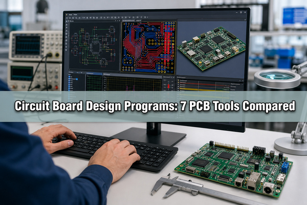
Circuit board design programs convert an electrical concept into schematics, component footprints, routed copper, design checks and production files. The right program is not simply the one with the longest feature list. It must support the board technology, team workflow and manufacturing data your project actually needs. This guide compares seven current PCB tools and explains how to select one without losing sight of fabrication and assembly requirements.

Circuit Board Design Programs: 7 PCB Tools Compared

What Are Circuit Board Design Programs?

Circuit board design programs are electronic design automation applications used to create the logical and physical definition of a printed circuit board. A complete PCB environment normally includes schematic capture, symbol and footprint libraries, component placement, copper routing, planes, vias, design-rule checking and fabrication outputs. Some suites add circuit simulation, signal-integrity analysis, mechanical co-design, supply-chain data or formal release management.

A drawing program is not automatically a PCB design program. A schematic-only tool may describe electrical connectivity without producing a routed board. A circuit simulator can predict electrical behavior but may not create manufacturing artwork. A Gerber viewer can inspect production files but cannot reliably reconstruct the editable source design. Confirm that a candidate tool covers the entire workflow you intend to own.

Which Features Matter in Circuit Board Design Software?

Start with the hardest requirement in the design, not the software brand. A two-layer controller may need only stable libraries, copper pours and basic DRC. A dense processor board can require differential-pair rules, impedance profiles, via constraints, length tuning, power-integrity review and controlled release data.

  • Schematic and library integrity: symbols, pin numbers, footprints, part numbers and assembly variants must remain synchronized.
  • Rules and constraints: trace width, spacing, drill size, annular ring, differential pairs, matched lengths and region-specific rules should be configurable.
  • Board technology: verify layer, blind/buried via, microvia, rigid-flex, high-speed and high-current support before starting the layout.
  • Verification: ERC, DRC, 3D clearance, connectivity and manufacturing-output viewers should expose errors before release.
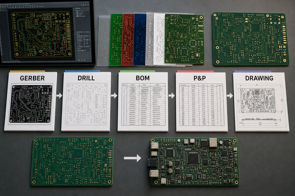
  • Manufacturing data: the program should generate consistent Gerber or intelligent product data, NC Drill, drawings and assembly files.
  • Collaboration: version control, comments, library governance and ECAD/MCAD exchange matter when several engineers share the project.
  • Lifecycle and licensing: confirm commercial-use rights, project privacy, supported operating systems and the cost of the required feature tier.

How Do Schematic Capture and PCB Layout Work Together?

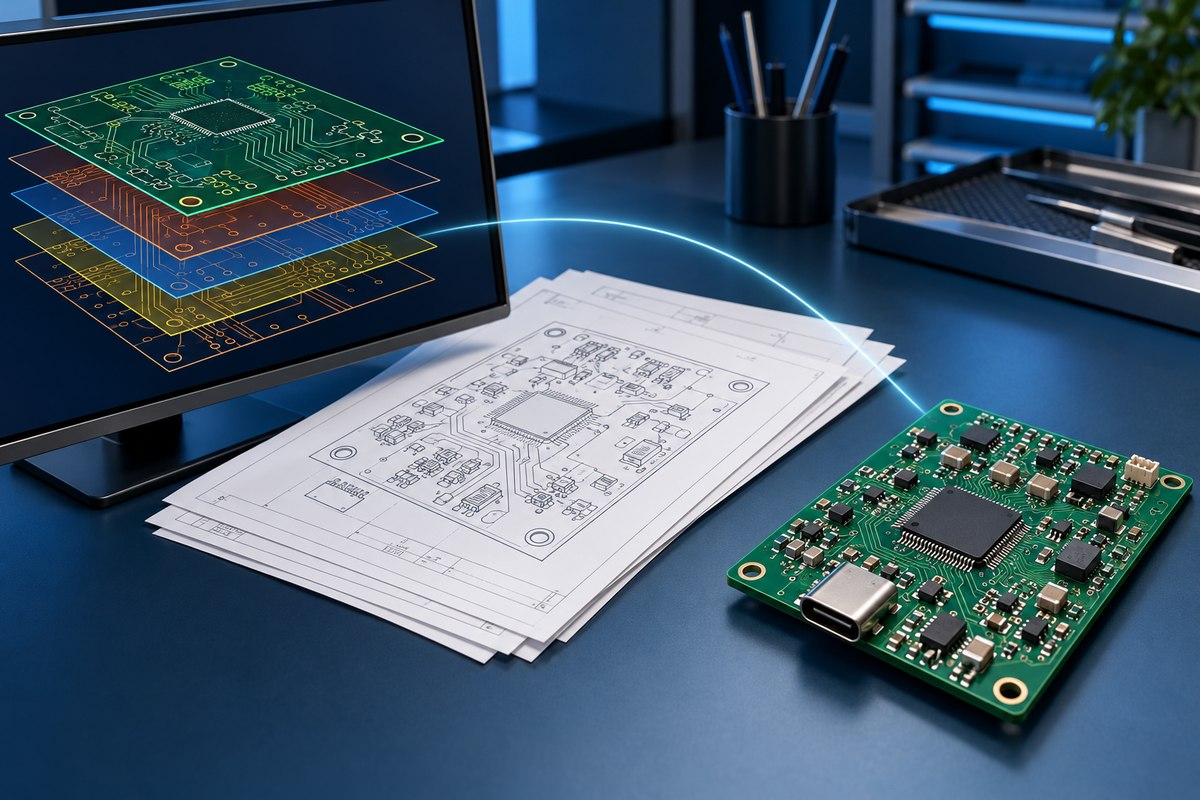
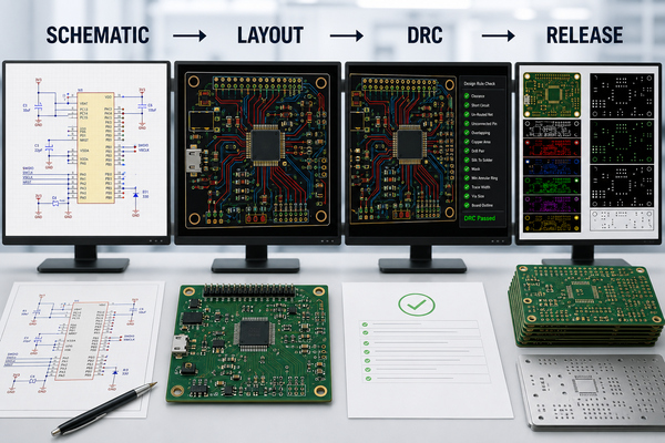
The schematic defines connectivity and design intent; the PCB editor turns that intent into physical geometry. A clean workflow assigns verified footprints, transfers networks to the board, defines the outline and stack-up, places components, routes critical signals, adds planes, runs checks and releases manufacturing data. Forward and backward annotation keep reference designators, net names and component changes aligned.

PCB design workflow from schematic capture to manufacturing release

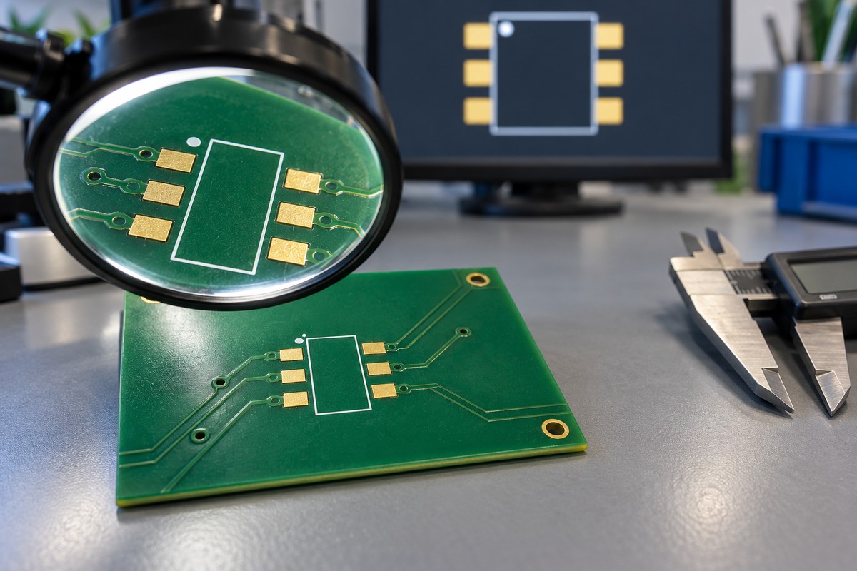
Footprint quality is a frequent source of physical errors. Check pad dimensions, hole sizes, pin-one orientation, courtyard clearance, paste openings and the component manufacturer’s recommended land pattern. A correct schematic symbol connected to an incorrect footprint can pass an electrical check and still produce an unusable assembly.

Which Circuit Board Design Programs Should You Compare?

The seven tools below represent distinct, current workflows. The table is a selection map, not a universal ranking. Product editions and licensing change, so confirm the current package before committing a project.

Program Best fit Key strength Check before adoption
Altium Designer Professional teams and complex boards Unified schematic, layout, 3D, constraints and release management Required license tier, training and workspace policy
KiCad Open-source commercial, startup and individual projects Cross-platform schematic/PCB workflow with Gerber and IPC-2581 Team library governance and collaboration process
Autodesk Fusion Electronics Products with close PCB-enclosure interaction ECAD and mechanical CAD coordination Cloud workflow, licensing and advanced constraint needs
Cadence OrCAD X Constraint-driven and high-speed design Electrical, physical, spacing, manufacturing and high-speed constraints Configuration effort and analysis modules
Siemens PADS Professional Professional boards, rigid-flex and ECAD/MCAD collaboration Routing, SI and integrated DFM options Current PADS-to-Xpedition product path and license scope
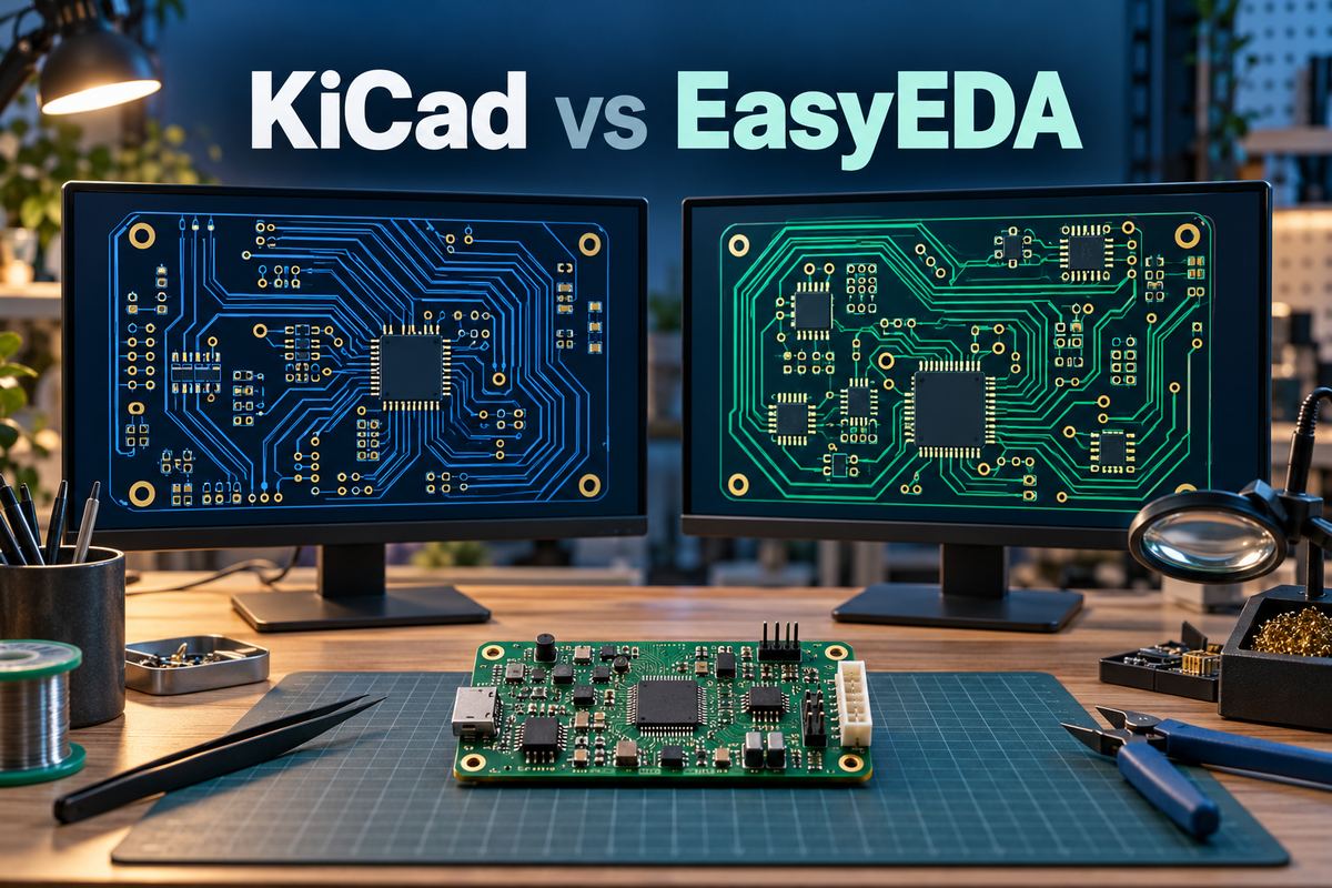
EasyEDA Fast online work, makers and distributed teams Browser access, large libraries and direct Gerber/BOM/Pick-and-Place export Cloud data policy and complex-rule requirements
LibrePCB Open-source projects needing readable project files Clean file format, DRC, 3D and command-line automation Library depth, importer limits and organization-specific features
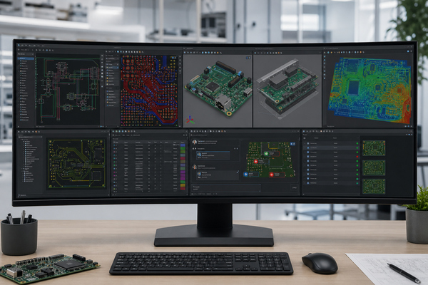
Comparison of seven PCB design software workflows

Altium Designer

Altium suits projects that need one environment for schematic capture, PCB layout, rigid-flex, advanced routing, 3D checking, BOM management and controlled manufacturing release. Its OutputJob and Project Releaser workflows can package fabrication and assembly data consistently. The main decision is whether the project complexity and team workflow justify the licensing and training investment.

KiCad

KiCad is a free, open-source, cross-platform EDA suite with integrated schematic and PCB editors, 3D viewing, Gerber output and IPC-2581 support. It can handle serious commercial designs when libraries, templates and reviews are managed carefully. Teams should define naming, version-control and library approval rules instead of assuming open-source software removes process requirements.

Autodesk Fusion Electronics

Fusion Electronics is attractive when the PCB, enclosure, connectors and mounting features must evolve together. ECAD/MCAD coordination can reduce outline, height and interference mistakes. Evaluate its electronics constraint depth separately from its mechanical integration, especially for dense high-speed or unusual stack-ups.

Cadence OrCAD X

OrCAD X provides structured electrical, physical, spacing, manufacturing and high-speed constraint management. That makes it useful when many net classes, interfaces or regional rules must remain controlled. The benefit depends on correct setup; a powerful constraint system with incomplete inputs will still release an incomplete design.


Siemens PADS Professional

PADS Professional supports professional PCB flow, mechanical collaboration, rigid-flex, signal-integrity options and design-for-manufacturing analysis. Siemens now directs new users to evaluate the upward-compatible Xpedition Standard path, so organizations should confirm the current product roadmap, data compatibility and module bundle before standardizing a new library.

EasyEDA

EasyEDA combines online schematic capture, PCB layout, DRC, component libraries, 3D viewing and common fabrication and assembly exports. It reduces setup time for straightforward projects and remote collaboration. For controlled commercial designs, verify workspace privacy, revision ownership, footprint approval and the limits of the selected edition.

LibrePCB

LibrePCB is a free, cross-platform suite with schematic-to-board synchronization, multilayer layout, DRC, 3D viewing and human-readable project files. Its CLI can support automated checks and exports in a version-controlled workflow. Confirm that its libraries, importers and output jobs cover the organization’s existing designs before migrating active products.

Which Free Circuit Board Design Software Is Best?

KiCad is the strongest general-purpose free choice when the project needs a complete offline EDA workflow and control over local source files. EasyEDA is often faster for browser-based learning and straightforward boards with online libraries. LibrePCB is useful when clean project files and command-line automation are priorities. For additional beginner-oriented options, see the existing guide to free PCB design software for beginners.

“Free” should be checked at three levels: software license, commercial-use rights and project visibility. A tool may cost nothing while requiring public projects, limiting board complexity or reserving advanced routing and collaboration for another tier. Review the current terms before placing proprietary designs or customer libraries in a cloud workspace.

What PCB Design Software Should You Use for Complex Boards?

Complex boards need constraint depth more than a long component list. For high-speed digital interfaces, look for stack-up-aware impedance rules, differential-pair control, length and delay tuning, return-path visibility and SI/PI integration. The high-speed digital PCB design guide explains how those rules connect to materials and fabrication tolerances.

For an HDI PCB, the software must define microvias, sequential buildup, via-in-pad, stacked or staggered structures and fabrication-specific annular-ring and capture-pad rules. A conventional via rule set is not enough.

A rigid-flex PCB also needs bend regions, layer transitions, coverlay, stiffeners, flex-specific clearances and a stack-up that distinguishes rigid and flexible zones. Choose a program and edition that model these structures explicitly rather than approximating them with drawing layers.

Should You Choose Online or Desktop PCB Software?

Online tools reduce installation effort and can simplify real-time collaboration. Desktop tools provide local processing, offline access and more direct control over project storage. Hybrid platforms combine desktop editors with cloud review, libraries and release management.

Decision factor Online or cloud-first Desktop or local-first
Access Fast from supported browsers and devices Restricted to installed systems unless remote access is arranged
Collaboration Comments, sharing and live updates may be built in Usually depends on version control, file management or a separate platform
Performance Depends on browser, connection and service capacity Uses local workstation resources
Data control Requires review of hosting, privacy, access and export policies Supports local storage but still needs backups and access control
Updates Service updates are generally automatic Organizations can qualify and deploy versions deliberately

Choose according to the project’s IP policy, collaboration model and validation process. Cloud is not automatically insecure, and local files are not automatically protected. Account permissions, backups, version history, approved libraries and release control matter in both models.

Which Manufacturing Files Must PCB Design Software Export?

A fabrication package must describe copper, solder mask, silkscreen, holes, board outline, stack-up and special requirements without contradictions. Gerber X2 or RS-274X plus NC Drill remains common, while IPC-2581 and ODB++ can carry more structured product data when both sides support the format.

  • Bare-board fabrication: Gerber or intelligent product data, plated/non-plated drill files, route data, fabrication drawing, stack-up and controlled-impedance information.
  • Assembly: BOM, centroid or Pick-and-Place file, assembly drawing, polarity/orientation details and approved component alternatives.
  • Mechanical verification: board outline, cutouts, height limits and STEP or another agreed 3D exchange format.
  • Validation: DRC/ERC reports, netlist or IPC-D-356 when appropriate, and a readme that identifies units, revisions and file purpose.
PCB manufacturing release files including Gerber drill BOM and Pick-and-Place

If the board will receive components, the manufacturing release should also match the needs of PCB assembly. Reference designators in the BOM, centroid file, assembly drawing and silkscreen must agree. Mismatched rotations, duplicate designators or unapproved package substitutions cannot be corrected by the bare-board Gerber set.

How Do DRC and DFM Differ?

DRC checks the layout against rules stored in the design program. It can detect spacing, width, drill, annular-ring, connectivity and other geometric violations. DFM checks the released design against an actual manufacturing process, material set, panel method and assembly capability. A design can pass DRC and still require changes because its rules were generic, outdated or incomplete.

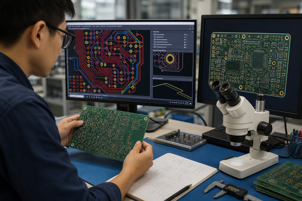
PCB design rule and manufacturability review on a routed circuit board

Configure the design program with values agreed for the intended construction. Do not use the software’s default minimum merely because it is available. A broader explanation of the factory-side checks is available in the guide to PCB manufacturing software and DFM.

How Can You Validate a PCB Design Before Fabrication?

  1. Run ERC and resolve unintended open pins, conflicting drivers and power-network errors.
  2. Verify every new or modified symbol and footprint against the current component datasheet.
  3. Run DRC with the actual stack-up, copper weight, drill and spacing limits.
  4. Inspect unrouted nets, copper islands, acute features, mask slivers and copper-to-edge clearance.
  5. Review the 3D model for connector location, polarity, height and enclosure interference.
  6. Generate the release package from a controlled revision, then inspect Gerber and drill data in an independent viewer.
  7. Cross-check the BOM, Pick-and-Place file and assembly drawing for reference-designator and rotation consistency.

Independent viewing matters because it checks the exported result rather than the editable source. Confirm units, zero suppression, drill mapping, layer names and the final outline. Releasing a correct project with an incorrect output configuration still creates incorrect manufacturing data.

Which PCB Software Fits Each Project Type?

Project type Software priority Practical starting point
Simple two-layer controller Stable libraries, basic DRC, Gerber and drill export KiCad, EasyEDA or LibrePCB
General multilayer FR4 Stack-up, planes, impedance rules and controlled release KiCad or a professional commercial suite
High-speed or dense HDI Constraint management, tuning, SI/PI and microvia rules Altium, OrCAD X or Siemens flow
PCB inside a tight enclosure ECAD/MCAD exchange, 3D clearance and height control Fusion Electronics or another tool with verified MCAD workflow
Rigid-flex product Region-specific stack-up, bend and coverlay support A professional edition with native rigid-flex features
Open-source automated workflow Readable files, version control and CLI checks KiCad or LibrePCB, after output validation

For a standard FR4 PCB, even a modest tool can produce a valid design if the libraries, stack-up and fabrication rules are correct. The selection changes when the board requires microvias, flex transitions, high-layer-count routing or specialized analysis.

What Should You Check Before Switching PCB Programs?

Test migration with a controlled copy of a representative project. Import the schematic, board, libraries and rules, then compare the result object by object. Neutral manufacturing formats preserve fabrication intent but are not a reliable substitute for editable source data.

  • Confirm that symbols, pin numbers, footprints and reference designators remain linked.
  • Check stack-up, net classes, differential-pair definitions, length rules and impedance constraints.
  • Inspect polygons, keepouts, rooms, variants, mechanical layers and custom pad shapes.
  • Regenerate DRC and manufacturing outputs instead of reusing files from the old tool.
  • Keep the original project and a documented conversion report until the new release is validated.

How Does EBest Circuit Support the Design-to-Manufacturing Handoff?

EBest Circuit (Best Technology) supports PCB design and layout, DFM review, prototyping, PCB fabrication, component sourcing and PCB assembly. For FR4 projects, published capabilities include boards up to 32 layers. HDI capability is advertised down to 2/2 mil line and space and 0.10 mm holes, subject to stack-up, board dimensions, materials and engineering review.

The useful handoff is a consistent design release, not a preferred native software brand. Supply the agreed fabrication and assembly outputs with revision control, while retaining editable source files for future changes. Engineering review can then compare the released geometry with the intended materials, copper, drill structure, impedance and assembly process.

FAQ About Circuit Board Design Programs

Is free circuit board design software suitable for commercial work?

Yes, a free tool can support commercial hardware if its license permits commercial use and it provides the rules, libraries and output formats the project requires. Verify current license terms, project privacy and edition limits before use.

Is Altium Designer free?

Altium Designer is a commercial product. Trial, education and related community offerings may have different terms, so check Altium’s current licensing page rather than assuming one entitlement covers commercial production.

Can PCB design software simulate a circuit?

Some EDA suites include SPICE or connect to dedicated simulation tools, but simulation coverage varies. Circuit simulation does not replace PCB layout checks, signal/power-integrity analysis, thermal review or prototype testing.

Can you move a PCB project between design programs?

Importers can move part of a project, but rules, libraries, polygons, variants and specialized objects may not translate completely. Validate the converted source and regenerate all manufacturing outputs before using it for a new revision.

What files does a PCB manufacturer need from design software?

For bare-board fabrication, provide the agreed Gerber or intelligent product-data package, NC Drill, outline, stack-up and fabrication notes. Assembly additionally needs a BOM, Pick-and-Place file and assembly drawing with consistent reference designators and orientation.

Do circuit board design programs replace engineering review?

No. The software checks the rules and models configured in the project. It cannot infer every material, fabrication, assembly, thermal, test or reliability constraint that was never entered.

Conclusion

Select circuit board design programs by matching their verified capabilities to the board technology, collaboration model and release data required. KiCad, EasyEDA and LibrePCB cover many accessible workflows, while Altium, OrCAD and Siemens tools add deeper control for complex projects; Fusion is especially relevant when mechanical integration drives the design. Whichever tool you use, validate libraries, rules and exported manufacturing files before release. For support moving a completed design into PCB fabrication and assembly, contact sales@bestpcbs.com.

You may also like

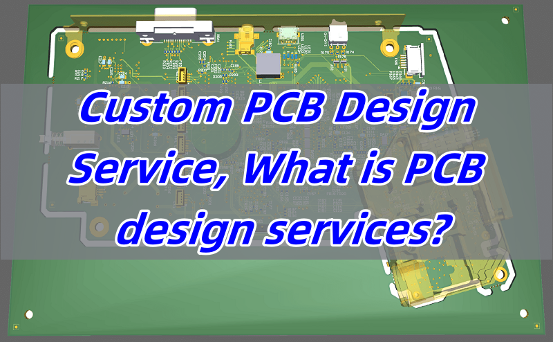
Custom PCB Design Service​, What Is PCB Design Services?
Tuesday, February 25th, 2025

PCB design services are essential for creating high-quality, functional circuit boards. In today’s world, printed circuit boards (PCBs) are a fundamental part of most electronics, from smartphones to medical devices and automotive systems. PCB design services play a crucial role in ensuring that these boards are functional, reliable, and efficient. But what exactly is PCB design, and how does it impact the electronics you use every day?

What is PCB Design Services?

PCB design services refer to the process of planning and creating a circuit board layout that connects different electronic components, ensuring they work together correctly. The design involves everything from schematic creation to the final layout of the PCB. PCB design is a specialized field that requires advanced knowledge of both electrical engineering and design software. The goal is to create a board that performs its intended function effectively while minimizing errors and ensuring ease of manufacturing. At EBest Circuit (Best Technology), our PCB design services are backed by 18 years of expertise, ensuring that every design is optimized for both performance and manufacturability, delivering reliable results for a wide range of applications

Does PCB Design Require Coding?

Many people assume that designing a PCB requires coding, but that’s not always the case. While some aspects of PCB design may involve programming—especially when designing components like microcontrollers or programmable logic devices (PLDs)—the main design process itself doesn’t necessarily require coding. Instead, it focuses on creating a layout of components on the board and ensuring that they are connected in the right way to function as intended.

That said, PCB designers do use software tools, which may include scripting languages or built-in code for specific tasks, like automating the routing process or checking for design rule violations. But for the most part, the core of PCB design is visual and structural, not a coding-heavy task.

Is PCB a CAD Design?

Yes, PCB design is essentially a form of computer-aided design (CAD). PCB design software allows designers to create a digital version of the circuit board before it is physically manufactured. CAD tools help with placing components, creating the electrical connections (traces), and optimizing the layout for factors like size, functionality, and manufacturability.

Some of the most popular PCB design software includes tools like Altium Designer, Eagle, and KiCad. These tools offer both 2D and 3D visualizations of the PCB, enabling designers to check for potential issues before sending the design to production. So, in a way, PCB design and CAD design are closely linked, with CAD software playing a key role in the process.

What Does a PCB Design Include?

A complete PCB design encompasses several crucial elements. First, the designer creates a schematic diagram that defines the electrical connections between components. This is followed by the layout phase, where the components are physically placed on the board, and the electrical traces (which act as wires on the PCB) are drawn.

Beyond the schematic and layout, PCB design also involves creating a bill of materials (BOM), which lists all the components that will be used. This document is critical for both manufacturing and sourcing the necessary parts. Additionally, designers must consider factors such as the board’s power requirements, signal integrity, and thermal management.

Some PCB design services also include testing and validation to ensure the design will perform as expected in real-world conditions.

How to Calculate PCB Design Cost?

The cost of PCB design services can vary significantly based on several factors. Generally, the complexity of the design, the size of the board, and the number of layers (single-layer, multi-layer) play a major role in determining the price.

Here are some key elements that can impact the overall cost:

Design Complexity: A simple PCB for a small electronic device will be cheaper to design than a multi-layer, high-frequency PCB.

Size and Layers: Larger boards or designs with more layers tend to be more expensive due to the added complexity.

Custom Components: If your design includes custom parts or components, it will increase the cost.

Prototype Testing: If you require prototypes for testing, this will add to the cost, especially if iterative testing and redesign are needed.

Typically, the cost is either an hourly rate for the designer or a flat fee per project. It’s important to discuss these factors with your PCB design service provider to get an accurate estimate.

Is PCB Design Difficult?

PCB design is a specialized skill, and like any engineering field, it can be challenging. Designers must have a deep understanding of electronics, the function of different components, and how they interact within a circuit. The process requires precision and attention to detail, especially when it comes to ensuring that components are properly connected, with no errors or potential for electrical shorts.

However, PCB design tools have advanced considerably over the years, making the process easier and more efficient. With the right tools and knowledge, designing a PCB can be a rewarding experience. For beginners, many software platforms offer tutorials, and professional design services are always available if the design process seems daunting. At EBest Circuit (Best Technology), our experienced team understands the intricacies of PCB design services, tailoring each project to meet both your functional and budgetary needs.

What Is the Difference Between PCB Design and Layout Services?

PCB design and PCB layout are often used interchangeably, but they refer to different aspects of the process. PCB design generally includes the creation of the circuit schematic and the overall functionality of the board. It’s about determining what components are needed and how they will be connected.

PCB layout, on the other hand, focuses on arranging the physical components on the board and routing the electrical connections. This stage involves translating the design into a practical layout that can be manufactured. The layout process also includes ensuring that the traces don’t overlap, the components fit, and that the board will meet performance requirements.

Both services are integral parts of creating a functional PCB, and many service providers offer both design and layout services as part of a complete package. With a strong focus on both PCB design and layout services, EBest Circuit (Best Technology) ensures that every step of the process is optimized for high performance and efficient manufacturing.

How Do PCB Design & Manufacturing Services Work Together?

PCB design and manufacturing services are closely linked, as the quality of the design will directly impact the ease and cost of manufacturing. In many cases, it’s beneficial to work with a provider that offers both design and manufacturing services, as they can ensure that the design is optimized for efficient production.

When PCB design and manufacturing work together, the design is specifically tailored to the capabilities of the manufacturer, ensuring that the finished product meets all specifications. This can reduce the likelihood of design errors, improve the quality of the board, and speed up the production process. Additionally, working with a single service provider can simplify communication and reduce potential delays.

How to Choose the Right PCB Design Service for Your Needs?

Choosing the right PCB design service provider is crucial for the success of your project. Here are some factors to consider when making your decision:

Experience and Expertise: Look for a service provider with a proven track record in your industry.

Tools and Software: Ensure they use the latest PCB design tools and software to ensure efficiency and quality.

Customization Options: If you need a custom PCB design, check if they offer tailored services to meet your specific requirements.

Testing and Prototyping: It’s important to select a provider who offers testing and validation of designs to ensure functionality before full-scale manufacturing.

Customer Support: Choose a company that provides good communication and support throughout the design and manufacturing process.

Choosing the right PCB design service is crucial, and at EBest Circuit (Best Technology), we provide custom solutions that are designed to match your unique requirements and ensure reliable, high-quality results.

In conclusion, PCB design services are an essential part of developing functional, high-quality circuit boards. From the initial schematic to the final layout and manufacturing, these services ensure that your electronics perform as expected. Understanding how PCB design works, the costs involved, and how to choose the right service can help you make informed decisions when developing your next electronic product.

At EBest Circuit (Best Technology), we offer comprehensive PCB design and manufacturing services, ensuring high-quality designs optimized for production. If you need a custom PCB design service, warm welcome to reach us at sales@bestpcbs.com.

You may also like

10 Best Free PCB Design Software for Beginners
Monday, December 2nd, 2024

What Is PCB Design Software?

If you’ve ever looked inside an electronic device, you’ve seen a Printed Circuit Board (PCB). It’s the green (or sometimes blue) board filled with tiny components like resistors, capacitors, and microchips. These boards are the backbone of modern electronics. But how are they designed? That’s where PCB design software comes in.

‌PCB Design software ‌ refers to a professional software tool for designing and manufacturing printed circuit boards (PCBs). These software typically include functions ranging from schematic design, layout, and routing to signal integrity analysis to help engineers and designers efficiently complete PCB design tasks.

10 Best Free PCB Design Software for Beginners

PCB design software helps you plan and create these circuit boards digitally. Instead of physically assembling components and wiring them, you can design everything on your computer. The software ensures that all the components are placed correctly and connected properly. For beginners, it offers a hands-on way to learn electronics without needing a lab full of expensive equipment. In this blog post, we will share the top 10 best free PCB design software, hope this is useful for you.

Why Is PCB Design Software Important?

PCB design software plays a key role in electronics development. It reduces manual errors by providing accurate layouts and component placements. Without it, designing a circuit would be tedious and prone to mistakes.

Firstly, ‌PCB design software can significantly improve the design efficiency. Through automated and intelligent tools, software can significantly improve the efficiency of circuit design, reduce design time, and thus reduce the overall development cost. For example, design software provides functions such as schematic input, circuit simulation, component library management, etc., to help designers efficiently complete complex circuit layout.

Secondly, ‌PCB design software can ensure the functionality and reliability of the circuit. Through simulation function, design software can simulate the working state of the circuit in the early stage of design, help engineers predict and optimize the performance, thus reducing the design risk. In addition, the software can perform signal integrity analysis and thermal management to ensure the performance of high-speed or high-frequency circuits and the safe operation of the circuit board.

Third, ‌PCB design software helps to reduce production costs. Through simulation and verification, engineers can find and solve potential problems before production, avoid errors in the production process, and thus reduce production costs. For example, the design software can generate Gerber files for manufacturing, drilling files, etc.

Finally, ‌PCB design software has a wide range of applications and needs in the market. With the continuous development of electronic technology, the market demand for PCB design software continues to grow. Especially in the consumer electronics industry, such as the highly complex circuit design of smart phones and smart wearables, makes PCB design software an indispensable tool.

10 Best Free PCB Design Software for Beginners

There are plenty of PCB design tools out there, but not all of them are beginner-friendly. Here’s a closer look at ten of the best free options, including their pros and cons.

1. KiCad

KiCad is a powerful, open-source PCB design tool that’s widely used by both hobbyists and professionals. It offers a comprehensive set of features, making it suitable for projects of all sizes.

Advantages:

Supports multi-layer designs: You can work on both simple and complex circuits.

3D viewer: It allows you to see a 3D model of your PCB, giving you a better sense of how it will look and fit into a device.

Extensive libraries: KiCad comes with a vast library of components, making it easy to find what you need.

Disadvantages:

Steep learning curve: The interface can be overwhelming for beginners, but once you get used to it, the possibilities are endless.

10 Best Free PCB Design Software for Beginners

2. Eagle Free

Eagle (Easily Applicable Graphical Layout Editor) has been a favorite among PCB designers for years. The free version, backed by Autodesk, is perfect for beginners.

Advantages:

User-friendly interface: The layout is intuitive, helping new users find their way around quickly.

Integration with Autodesk tools: If you use other Autodesk products, Eagle fits right into your workflow.

Component libraries: It offers a vast selection of components and symbols.

Disadvantages:

Limitations in the free version: You can only create boards with a limited size and two signal layers. Upgrading to the paid version removes these restrictions.

10 Best Free PCB Design Software for Beginners

3. EasyEDA

EasyEDA is a cloud-based PCB design tool that’s growing in popularity. It’s an excellent choice for beginners who want a straightforward, accessible platform.

Advantages:

No installation required: Since it’s cloud-based, you can use it from any device with a browser.

Component libraries: EasyEDA connects directly to component suppliers, making it easy to find and order parts.

Community-driven: It has an active community where users share designs and offer help.

Disadvantages:

Internet dependency: You need an internet connection to use it, which can be a drawback for offline work.

10 Best Free PCB Design Software for Beginners

4. Fritzing

Fritzing is designed specifically with beginners in mind. It offers a unique approach by allowing you to design circuits in a breadboard view before moving to a PCB layout.

Advantages:

Beginner-friendly interface: The drag-and-drop design makes it easy to use, even if you have no prior experience.

Educational focus: Fritzing is often used in educational settings, making it a great learning tool.

Disadvantages:

Limited advanced features: It’s ideal for simple projects but may not be suitable for more complex designs.

10 Best Free PCB Design Software for Beginners

5. GerbView

GerbView is a free Gerber file viewer that allows you to visualize, verify, and print your PCB layouts. While it doesn’t offer full PCB design capabilities, it’s a crucial tool for inspecting and validating your designs before sending them to a manufacturer.

Advantages:

Comprehensive file support: GerbView supports various file formats, including Gerber, Excellon, and HPGL files, making it versatile for different PCB layouts.

Accurate visualization: You can zoom in and inspect even the smallest details, ensuring your design is error-free.

Conversion tools: It can convert older Gerber files to modern formats and export designs to PDF or other formats for documentation.

Disadvantages:

Not a full PCB design tool: It’s mainly a viewer and validator, so you’ll need another tool for designing your PCB.

Limited editing options: While you can inspect and highlight areas, you can’t modify the actual PCB design within GerbView.

10 Best Free PCB Design Software for Beginners

6. CircuitMaker

CircuitMaker, developed by Altium, offers professional-grade tools for free. However, there’s a catch: your designs are shared publicly.

Advantages:

Professional-level features: You get access to high-end design tools without paying a dime.

Collaboration-friendly: It’s designed for makers and hobbyists who want to collaborate on projects.

Disadvantages:

Public designs: If privacy is a concern, this might not be the best option for you.

10 Best Free PCB Design Software for Beginners

7. PCBWeb Designer

PCBWeb Designer is a simple, Windows-only PCB design tool that’s easy to learn and use.

Advantages:

Straightforward interface: It’s clean and easy to navigate, making it perfect for beginners.

Component sourcing: It integrates with Digi-Key, allowing you to source components directly from the software.

Disadvantages:

Limited to Windows: If you use a different operating system, you’ll need to look elsewhere.

10 Best Free PCB Design Software for Beginners

8. Upverter

Upverter is another cloud-based PCB design tool, but it focuses heavily on collaboration.

Advantages:

Real-time collaboration: Multiple users can work on the same project simultaneously.

Cross-platform: Since it’s cloud-based, you can use it on any device with a browser.

Disadvantages:

Learning curve: Some users find the interface less intuitive than desktop-based tools.

10 Best Free PCB Design Software for Beginners

9. TinyCAD

TinyCAD is a lightweight, open-source tool focused on schematic capture rather than PCB layout.

Advantages:

Simple and fast: It’s easy to use, even on older computers.

Community-supported: As an open-source tool, it’s regularly updated and improved.

Disadvantages:

Limited PCB features: You may need to pair it with another tool for full PCB design capabilities.

10 Best Free PCB Design Software for Beginners

10. ZenitPCB

ZenitPCB is a straightforward PCB design tool that’s great for beginners.

Advantages:

Easy to learn: The interface is simple and user-friendly.

Lightweight: It runs smoothly on most systems, even older ones.

Disadvantages:

Limited advanced features: It’s best for basic designs and may not meet the needs of more complex projects.

10 Best Free PCB Design Software for Beginners

Factors to Consider When Choosing PCB Design Software

When selecting PCB design software, it’s important to consider your needs and experience level. Here are a few key factors:

  • Functional requirements

Different PCB design software has different functions, such as wiring, component libraries, rapid prototyping, etc. When choosing software, you need to choose the software that has the functions suitable for your needs ‌ according to your own needs.

  • Ease of use

Choosing PCB design software that is easy to use can improve work efficiency and reduce learning costs. Some software provides video tutorials, online help and other functions, which can help users learn how to use the software faster.

  • Compatibility

Choosing PCB design software that is compatible with other software can improve work efficiency. If you need to import the PCB design file to other software for simulation or other operations, select the PCB design software that is compatible with other software.

  • ‌4. Industry demand

Different industries may have different requirements for PCB design. For example, consumer electronics designs may prefer to use PADS, while complex large board designs may be better suited to Allegro‌.

FAQs About PCB Design Software

1. Can I use free PCB design software for professional projects?

Yes, many free tools allow commercial use. However, always check the license terms.

2. What’s the easiest PCB design software for beginners?

Fritzing and EasyEDA are excellent options for beginners due to their user-friendly interfaces.

3. Is cloud-based PCB design software secure?

Most cloud-based tools use encryption to protect your data, but it’s always a good idea to read the privacy policy.

4. Can I design multi-layer PCBs with free software?

Absolutely! Tools like KiCad and DesignSpark PCB support multi-layer designs.

5. How long does it take to learn PCB design?

With consistent practice, you can learn the basics in a few weeks. More complex designs may take longer.

Getting started with PCB design doesn’t have to be complicated. With the right software, you can bring your electronic ideas to life, whether you’re a beginner or an experienced hobbyist. Happy designing!

You may also like