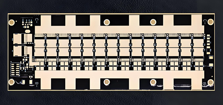
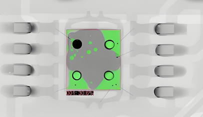
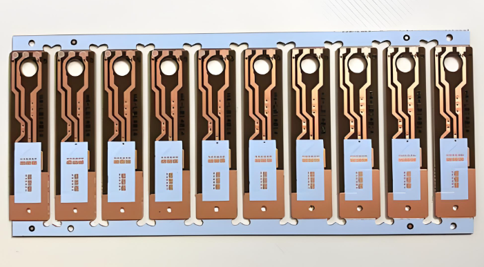
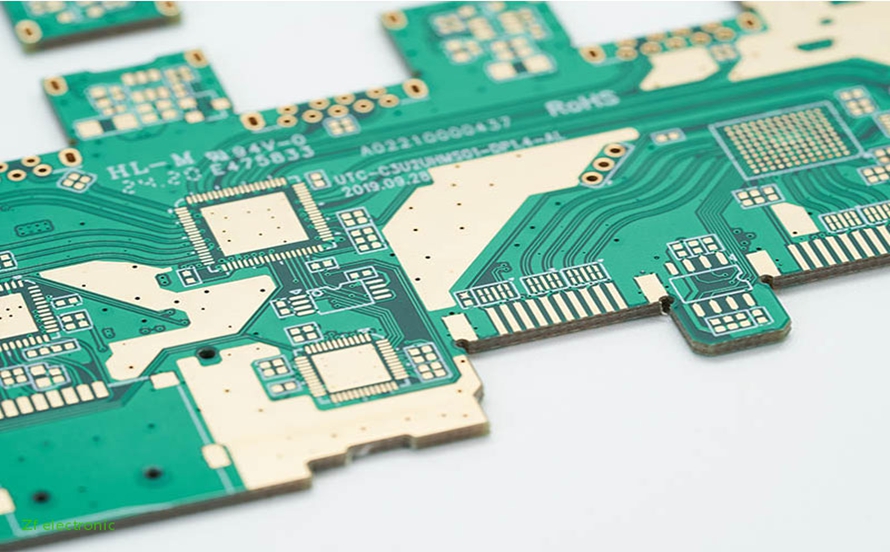
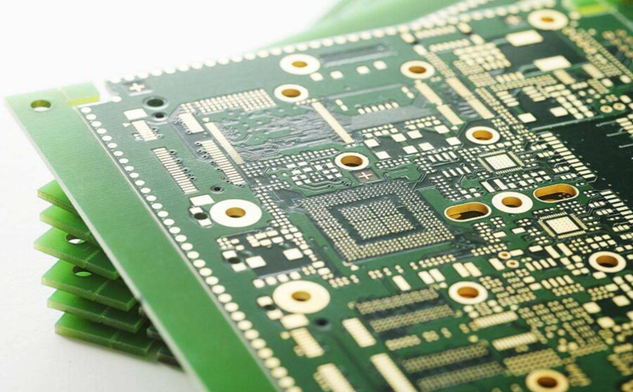
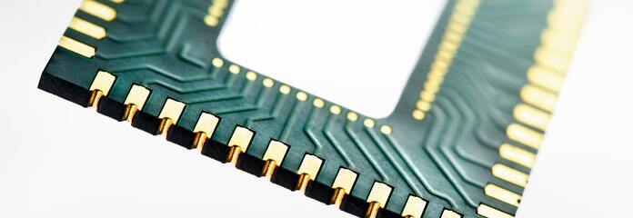
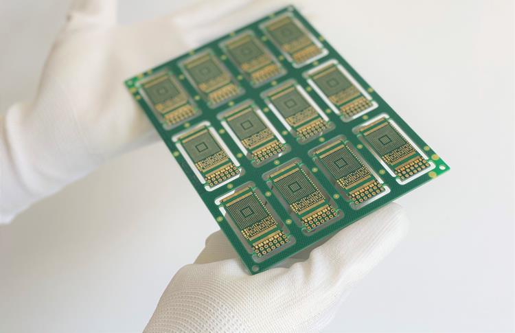
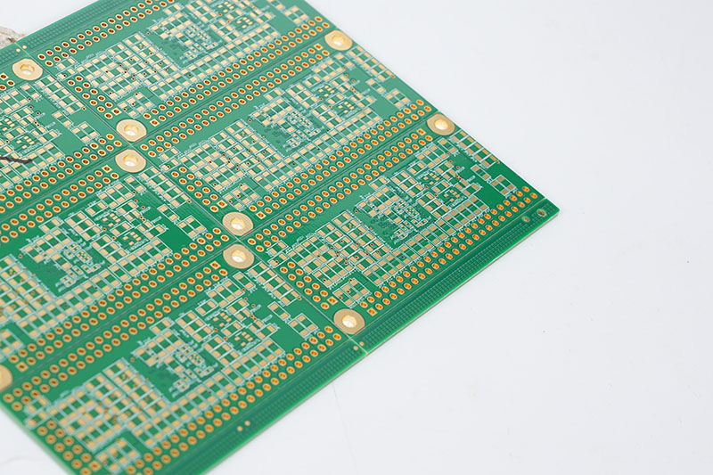
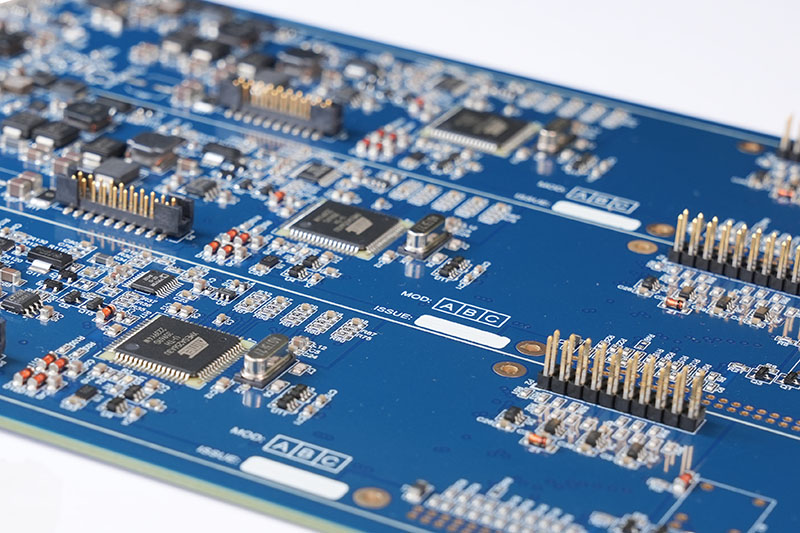
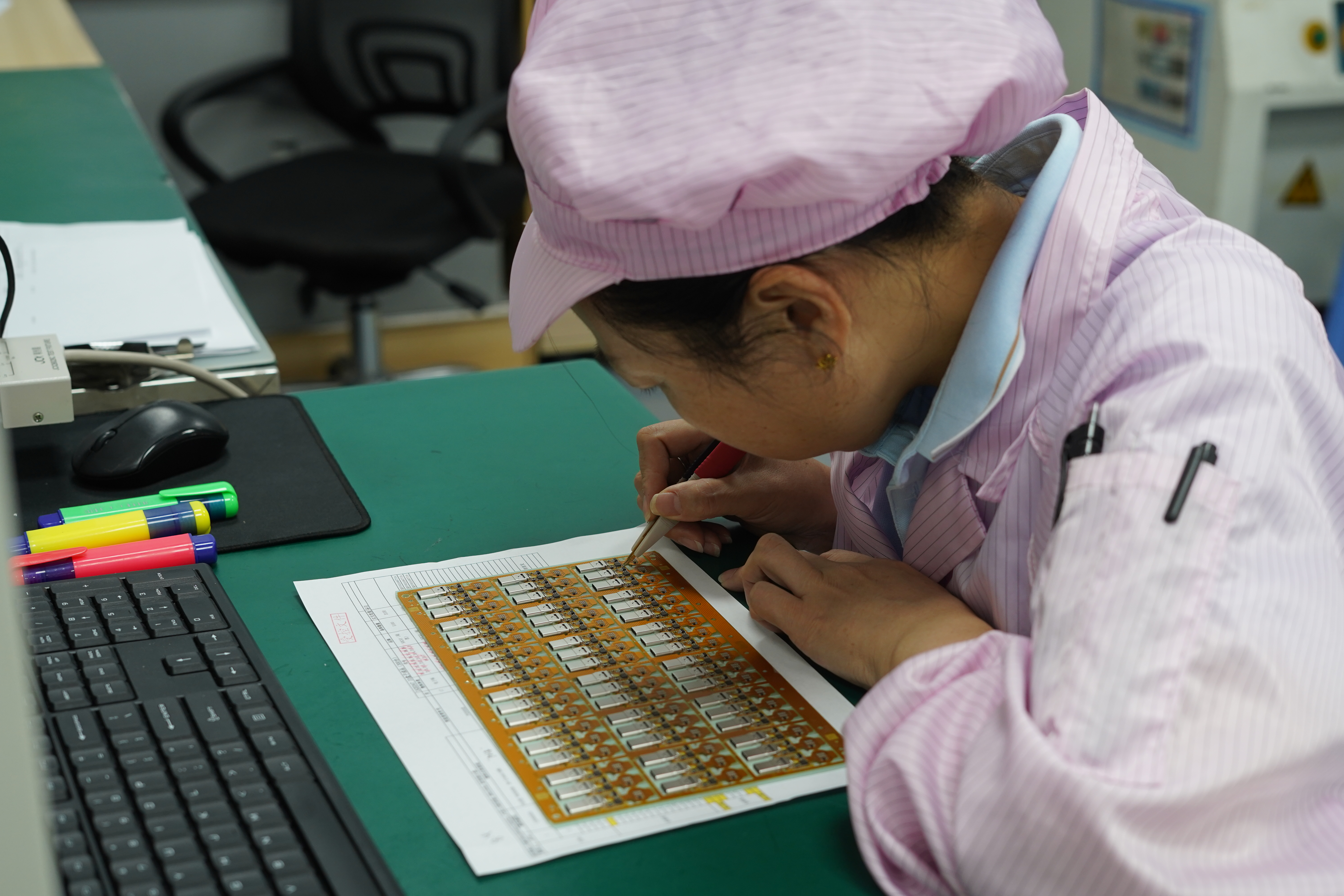
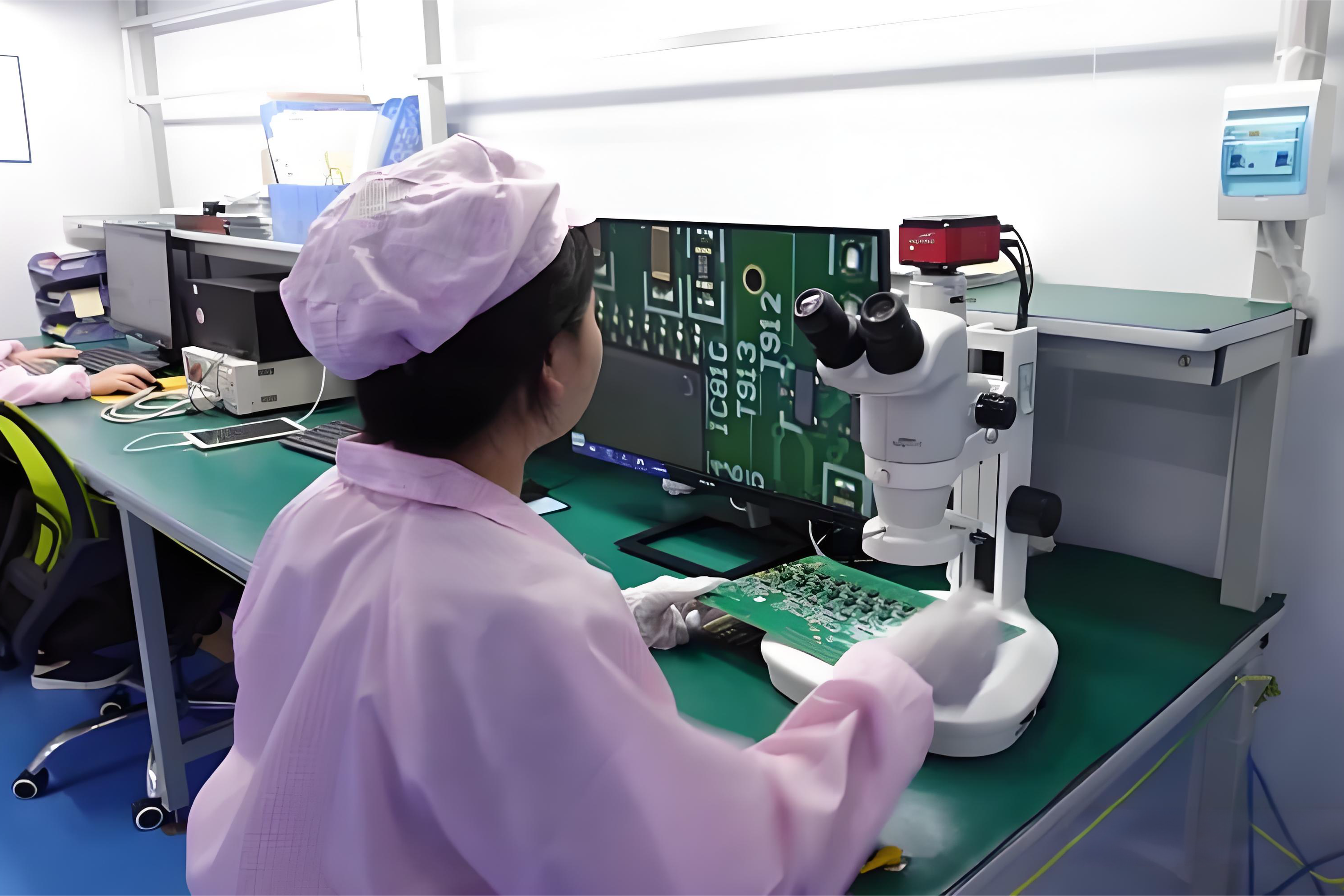
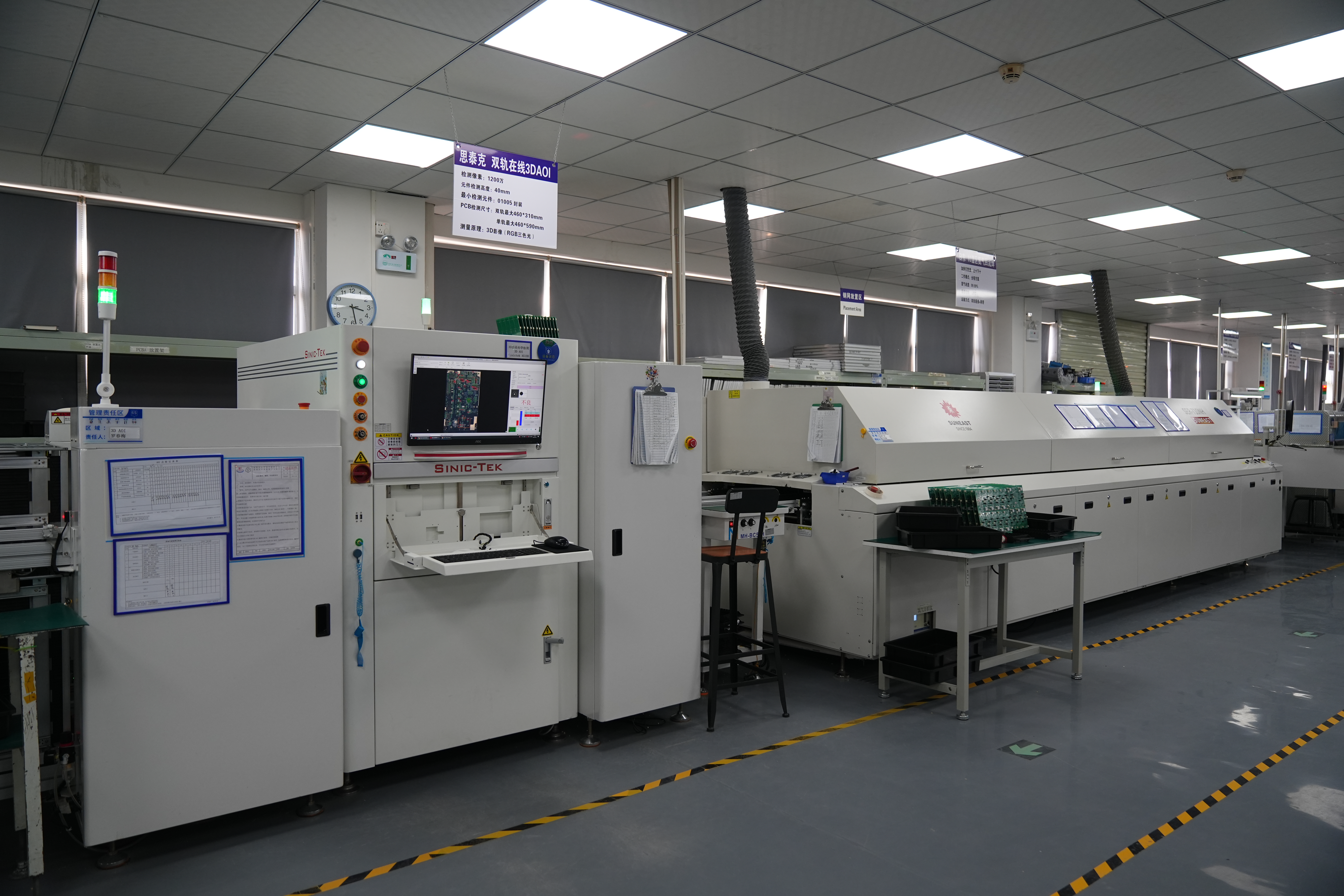
The copper busbar manufacturing process combines heavy-copper PCB techniques with precise metalwork. It begins with careful design to control current and heat. Pure copper sheets or bars are cut, cleaned, and prepared for bonding.
During lamination or bar insertion, the copper forms a solid low-resistance path inside the PCB stack. CNC drilling and routing create exact holes and outlines. Plating with tin, nickel, or silver protects the surface and improves soldering.
Finally, each board is tested for conductivity, flatness, and insulation strength. This streamlined process delivers reliable, high-current PCBs for demanding power-electronics applications.
EBest Circuit (Best Technology) has nearly 19+ years of experience in PCB manufacturing, offering a one-stop service for bus bar PCBs from layout design, diagram evaluation, prototyping and mass production to after-sales service. We are certified by ISO9001, ISO13485, IATF16949, and UL, ensuring high-quality PCBs with fast delivery. As experts in bus bar PCB manufacturing, custom bus bar PCBs are available according to your specific requirements.
What is copper busbar PCB?
Copper busbar PCB is a printed circuit board with thick copper layers or inserted copper bars that move high current. It is different from a normal PCB.
Traditional boards handle small to medium current. A bus bar PCB carries far more power while keeping temperature under control.
Engineers place a solid copper bar or heavy copper layer inside the PCB stack-up. Applications include renewable energy systems, electric vehicles, industrial drives, and telecom power units. These fields need a safe, low-loss path for energy.
What is the raw material of copper busbar?
The key ingredient is pure copper with a high conductivity grade. Most manufacturers use C1100 or equivalent electrolytic tough pitch copper.
This type of copper contains more than 99.9% purity. It resists oxidation and carries current with minimal loss.
For insulation, makers use FR-4, polyimide, or other high-temperature PCB substrates. Epoxy resins with strong bonding power hold the layers together.
Surface finishes such as nickel, tin, or silver plating protect the copper from corrosion. The choice depends on the end use.
BEST Technology sources these materials only from certified producers. Stable raw stock ensures each busbar meets strict electrical and mechanical requirements.
How to make a copper busbar?
The copper busbar manufacturing process blends PCB technology with precision metalwork. Here is a clear view of the main stages:
1. Design and Simulation
Engineers design the current path and thickness. They run thermal and electrical simulations.
2. Copper Cutting and Preparation
High-purity copper sheets or bars are cut to exact size. Any surface oxide is removed.
3. Lamination or Bar Insertion
Two common methods exist.
Heavy copper lamination adds extra copper layers during PCB pressing.
Bar insertion places a pre-machined copper bar inside the board.
Both create a strong, continuous conductor.
4. Drilling and Routing
Precise CNC drilling forms mounting holes and routing channels.
5. Plating and Surface Finish
Nickel, tin, or silver is plated on exposed copper. This guards against oxidation and improves solderability.
6. Solder Mask and Legend
A protective solder mask covers non-conductive areas. Markings identify polarity and connection points.
7. Testing and Inspection
Manufacturers test current capacity, insulation resistance, and thermal rise. Only boards that meet design specs move forward.
Each stage demands strict process control. High-power electronics cannot tolerate flaws. Experienced copper bus bar manufacturers BEST TECHNOLOGY use advanced equipment to keep every parameter consistent.
What matters most in Copper Bar Production for PCBs?
Several factors decide final quality:
Conductivity: Copper purity is critical.
Thickness: Adequate thickness handles the required amperage without excessive heat.
Flatness: Perfectly flat bars ensure tight contact with PCB layers and connectors.
Compact Design: High current moves through smaller space, reducing overall footprint.
High Reliability: Strong copper core resists fatigue and vibration.
Cost Efficiency: Fewer parallel traces and connectors lower assembly time.
These advantages matter in heavy-duty power electronics. Solar inverters, battery systems, and EV chargers need reliable high current flow every day.
Why should you use a bus bar PCB for power electronics?
Power electronics depend on efficient current distribution. A bus bar PCB cuts energy loss and enhances thermal performance.
Instead of routing multiple wide traces, designers integrate a single copper bus. This reduces connection points and lowers risk of loose joints.
The solid copper path also handles sudden current spikes. Equipment stays stable under load changes.
Maintenance becomes simpler. The board lasts longer with fewer hot spots and less stress on components.
What are the applications of Bus Bar PCB?
You will find bus bar PCBs across many industries:
Electric Vehicles: Battery management and drive inverters.
Renewable Energy: Solar power inverters and wind turbines.
Industrial Equipment: High-power motor controls and automation systems.
Telecom and Data Centers: Power distribution units for stable uptime.
Medical Devices: Imaging systems that demand steady high current.
In every case, heavy copper boards secure strong performance and safe operation.
Conclusion:
Copper busbar PCB offers unmatched power handling, heat control, and reliability. From pure copper raw materials to careful plating, every step of the copper busbar manufacturing process must meet strict standards.
EBest Circuit (Best Technology) Co., Ltd. is one of the trusted copper busbar manufacturers with factories in China and Vietnam. We deliver quick lead times, high precision, and competitive pricing. Our team provides a free first sample and 24-hour technical response.
For detailed specifications or a custom quote, reach out to sales@bestpcbs.com
What is a HDI multilayer PCB? Let’s discover its stackup, applications, technical parameter, design guide and manufacturing process through this blog.
Are you troubled with these problems?
Struggling with sub-0.1mm microvia fabrication in traditional PCB processes?
Facing high costs from signal loss in high-speed products?
Delayed by slow 8+ layer HDI prototyping impacting launches?
As a HDI multilayer PCB manufacturer, EBest Circuit (Best Technology) can provide you service and solutions:
Microvia Precision: 0.05mm laser-drilled vias with plasma treatment for compact designs.
Signal Stability: End-to-end SI/PI support for 10Gbps+ stable transmission.
Rapid Prototyping: 7-day standard lead time for 8-layer HDI, 5 days for urgent orders.
Welcome to contact us if you have any request for HDI multilayer PCB: sales@bestpcbs.com.

What Is a HDI Multilayer PCB?
HDI Multilayer PCB (High-Density Interconnect Multilayer Printed Circuit Board) is an advanced circuit board that employs precision microvias (aperture β€0.15mm), blind/buried via technology, and ultra-fine lines (line width/spacing β€3mil). Through laser drilling and layer-by-layer stacking processes, it achieves high-density routing across 8 or more layers within compact spaces. This design enhances signal transmission speed, reduces interference, and is specifically engineered for miniaturized, high-performance applications such as 5G devices and wearable electronics.
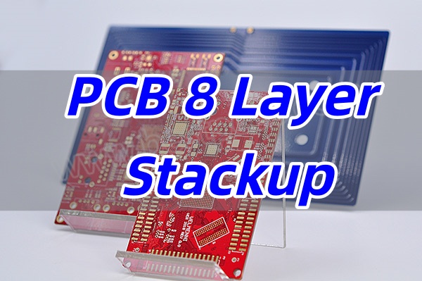
8 Layers HDI PCB Stackup
Layer
Layer Type
Main Function
Connection Method
L1
Signal Layer
High-frequency signal transmission / Critical component routing
Surface Blind Via (Connecting to L2)
L2
Power/Ground Plane
Power distribution / Ground network
Buried Via (Connecting to L3-L6), Blind Via (Connecting to L1/L3)
L3
Signal Layer
Inner-layer high-speed signal routing
Buried Via (Connecting to L2/L4)
L4
Signal Layer
Inner-layer control signal routing
Buried Via (Connecting to L3/L5)
L5
Signal Layer
Inner-layer low-speed signal routing
Buried Via (Connecting to L4/L6)
L6
Power/Ground Plane
Power distribution / Ground network
Buried Via (Connecting to L5/L7), Blind Via (Connecting to L7)
L7
Signal Layer
Inner-layer auxiliary signal routing
Blind Via (Connecting to L6/L8)
L8
Signal Layer
High-frequency signal transmission / Critical component routing
Surface Blind Via (Connecting to L7)
What Are Applications of HDI Multilayer PCB?
Applications of HDI multilayer PCB:
Smartphones & Mobile Devices: Mobile phone motherboard, Camera module, Sensor module, Antenna system, Automotive Electronics.
Engine Control Unit (ECU): In-vehicle navigation system, Airbag control module, Advanced Driver Assistance System (ADAS), In-vehicle entertainment system.
Medical Equipment: MRI imaging equipment, Cardiac pacemaker, Implantable medical devices, Precision diagnostic instruments, Communication Equipment.
5G base station: Router/switch, Fiber optic communication module, Satellite communication equipment.
Industrial Control: Industrial robot control board, PLC control system, Automated sensor network.
Servers & Data Centers: High-performance server motherboard, Cloud computing hardware, Data storage devices.
Place high-speed signals on outer layers (trace width/space β€4mil) with microvias (60-150ΞΌm laser-drilled) for layer-to-layer connections.
Use buried vias for interlayer routing (e.g., 1-2 layer blind via + 3-4 layer buried via) and select materials like Rogers 5880 (Dk=2.2) for high-frequency scenarios or FR4-Tg180 for thermal stability.
3. Intelligent Component Placement with Thermal Optimization
Center critical components (e.g., BGA-packaged CPU/FPGA) and position heat-generating devices near thermal via arrays.
Use “escape routing” from BGA centers to minimize trace length. Implement grid-pattern thermal vias (β₯150 vias/inchΒ², 0.3mm diameter, 1.0mm spacing) and thermal interface materials (TIMs) with β₯5W/mΒ·K conductivity for efficient heat dissipation.
4. High-Speed Signal Routing with Strict Rules
Enforce differential pair length matching (β€2mil difference) using serpentine routing for via delay compensation (bend radius β₯3Γ trace width).
Avoid crossing power splits to reduce crosstalk. Use stacked microvia structures (e.g., VIA1-2 + VIA2-3) for higher routing density and impedance continuity at connectors via “cross-connection + ground shield” (3Γ trace width spacing) with GND via pairs β€3mm apart.
Apply ENIG/ENEPIG surface finish (β₯3ΞΌm thickness) to prevent oxidation and use X-ray inspection for solder joint voids <10%.
8. Comprehensive Design Rule Verification
Execute DRC checks (line width/space, via dimensions, impedance compliance) per IPC-6012 Class 3 standards.
Collaborate with PCB manufacturers( like EBest Circuit (Best Technology)) for DFM analysis: confirm minimum trace/space 3mil, laser drilling accuracy Β±10ΞΌm, and process margins (etching tolerance Β±0.5mil).
9. Standardized Manufacturing File Generation
Output Gerber (RS-274X), drill (Excellon), solder mask, and BOM files with precise version control. Include assembly-specific annotations (e.g., polarity marks, fiducial placement) to streamline manufacturing.
10. Prototype Testing & Iterative Optimization
Conduct electrical tests (flying probe for impedance continuity), thermal tests (infrared thermography for hotspot mapping), and mechanical tests (vibration/shock for reliability).
Refine designs based on test results (e.g., topology adjustments, additional decoupling capacitors) and prepare for mass production with cost-optimized processes (resin-plugged vias) and quality control measures (AOI/X-ray inspection).
How Are Multilayer HDI PCBs Made?
Manufacturing processes for multilayer HDI PCBs:
1. Inner Layer Substrate Cutting & Pretreatment: Cut high-speed substrates (e.g., FR4, Rogers RO4350B) to design dimensions. Perform chemical cleaning to remove surface oxidation and contaminants, enhancing adhesion between copper layers and prepreg.
2. Inner Layer Pattern Transfer & Etching: Apply dry film, transfer circuit patterns via UV exposure and development. Etch unprotected copper using alkaline solution, followed by AOI (Automated Optical Inspection) to verify circuit integrity.
3. Brown Oxidation & Stack Alignment: Treat inner copper surfaces with brown oxidation to create nano-scale roughness. Stack inner layers, prepreg sheets, and copper foils in sequence, secured with rivets to prevent layer misalignment.
4. Vacuum Hot Pressing: Execute three-stage pressing (heating β main pressure β cooling). Gradually raise temperature at 2-3β/min to Tg point under 20-35kg/cmΒ² pressure, ensuring resin fills voids without cavities.
5. Laser Microvia Drilling: Use UV/COβ lasers to drill blind/buried vias with diameter β€0.15mm and depth tolerance Β±0.05mm. Clean hole walls via plasma desmear to remove drilling debris.
6. Via Plating & Filling: Deposit copper electrolessly on via walls, then electroplate to 8-12ΞΌm thickness. Implement via-filling plating (e.g., copper paste) to eliminate voids in blind/buried vias, ensuring reliable electrical conduction.
7. Outer Layer Patterning & Etching: Repeat inner layer processes, apply dry film, expose, develop, and etch to form high-precision lines (width/spacing β€3mil). Strip tin to retain circuit traces and via walls.
8. Solder Mask Printing & Curing: Print UV-curable solder mask ink to protect non-soldering areas. Expose and develop to reveal pads and test points, ensuring soldering reliability.
9. Surface Finish Selection: Apply ENIG (electroless nickel immersion gold), OSP (organic solderability preservative), or ENEPIG (electroless nickel electroless palladium immersion gold) based on application requirements, enhancing corrosion resistance and high-frequency signal integrity.
10. Reliability Testing: Conduct thermal shock (-55β~125β cycles), humidity resistance (85β/85%RH), vibration (β₯5G random), and electrical tests (flying probe/4-wire Kelvin testing) to meet IPC-6012 standards and client specifications.
11. CNC Profiling & V-Scoring: Shape boards via CNC routing, implement V-groove scoring for easy separation, ensuring edge dimensional accuracy β€Β±0.1mm without burrs or delamination.
12. Final Inspection & Packaging: Perform FQC (Final Quality Control) to check for defects, dimensional tolerances, and electrical performance. Vacuum-pack products to prevent moisture/oxidation during transport and storage.
Cost-Sensitive Design Solutions: Offer tiered pricing systems and material substitution options, optimizing trace width/spacing and substrate selection (e.g., FR-4/high-frequency material ratios) to reduce per-board costs by 10%-15% while ensuring performance, ideal for price-sensitive products like consumer electronics and IoT devices.
24-Hour Rapid Prototyping: Establish dedicated green channels for end-to-end tracking from design file receipt to sample delivery, supporting real-time online progress queries. For urgent needs like prototype validation or exhibition samples, achieve “same-day order placement, next-day shipment” to shorten iteration cycles to 1/3 of traditional timelines.
99.2% On-Time Delivery Rate: Leverage intelligent production scheduling systems and localized supply chain layouts, combined with dynamic inventory alerts, to ensure 10-15 day delivery for regular orders and 5-7 day delivery for urgent orders. Historical data confirms over 99.2% of orders meet agreed timelines, supporting clients’ production plans and market windows.
Full-Batch Quality Inspection: Employ dual AOI+X-ray inspection systems to verify 20+ critical parameters including trace width/spacing, hole precision, and impedance matching, alongside electrical testing and thermal shock trials. All batches meet IPC-6012 standards with defect rates below 0.08%.
International Authoritative Certification System: Hold ISO 9001, IATF 16949 (automotive), ISO 13485 (medical), and RoHS certifications, enabling global market compliance and reducing re-certification costs for clients targeting EU, North America, and Japan.
19 Years of HDI Technical Expertise: Accumulate over 5,000 HDI process case databases across 19 years, covering mobile, server, and medical sectors. The production error database proactively mitigates 90%+ potential issues, minimizing client trial costs.
Free DFM Design Optimization: Provide end-to-end manufacturability analysis from schematics to Gerber files, including package compatibility checks, routing topology refinement, and impedance matching suggestions, to identify design flaws early, shorten manufacturing cycles, and lower redesign expenses.
Multi-Tier Material Supply Chain: Strategic partnerships with suppliers like Rogers, Panasonic, and Shengyi ensure stable supply of high-frequency/high-speed materials and eco-friendly substrates, while centralized procurement reduces material costs for clients.
How to Get a Quote for HDI Multilayer PCB Project?
All files needs to be submitted to get a quote for HDI multilayer PCB:
Gerber Files: Include circuit design data for all layers (e.g., signal layers, power layers, silkscreen layers), with annotations for stack-up sequence, impedance-controlled traces, blind/buried via positions, and special process requirements (e.g., via-in-pad, resin plugging).
BOM (Bill of Materials): Detail component models, package dimensions (e.g., 0201/0402/QFN), supplier information, tolerance grades (e.g., Β±1% resistors), and material codes, ensuring alignment with component positions in Gerber files.
Special Process Requirements: Indicate needs for via-in-pad, back-drilling, stacked blind/buried vias, high-frequency material applications, thermal management solutions (e.g., thermal via arrays), or EMC protection measures (e.g., three-stage filtering).
Quantity & Lead Time Requirements: Provide batch order quantities (e.g., 500 pieces/batch), urgent order needs (e.g., 24-hour prototyping), standard lead time expectations (e.g., 10-15 days), and packaging specifications (e.g., vacuum packaging + anti-static bags).
Quality Certification & Testing Needs: List applicable international standards (e.g., IPC-6012, ISO 9001), specific test items (e.g., flying probe impedance testing, β₯1000 thermal shock cycles), and acceptable defect rate thresholds (e.g., β€0.08%).
Design File Version & Revision History: Include the latest design file version number, revision history, and design change notes to ensure manufacturing accuracy and timeline.
Welcome to contact us if you have any request for HDI multilayer PCB board: sales@bestpcbs.com.
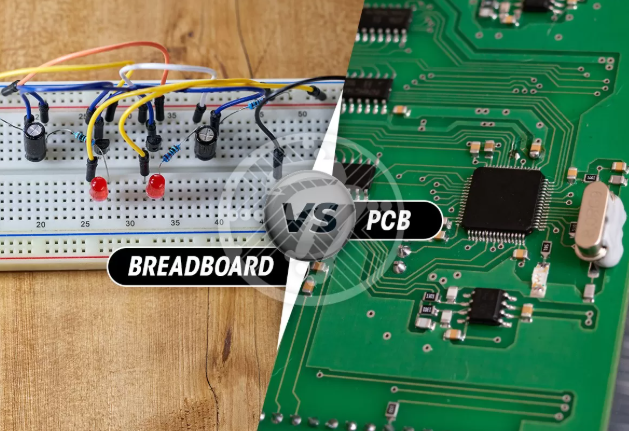
As a LED MCPCB Manufacturerβ, We are proud to provide a wide variety of MCPCBs for the lighting world. With over 19 years of experience in designing and manufacturing MCPCBs, we take pride in being your one-stop supplier.
As a trusted supplier, we hold certifications including UL, ISO13485, ISO9001, IATF16949 and SGS, enabling us to meet the high standards of clients across Europe, America, Israel, India, and so on. Explore our services and let us help you fulfill your MCPCB needs.
Are you looking for LED MCPCB Manufacturer? Do you have any questions?
What types of MCPCBs do you mainly produce?
Do you support customized designs?
What is the typical delivery time? Do you offer expedited service?
What after-sales service and technical support do you provide?
As a MCPCB manufacturer with 19+ years of experience, BEST Technology can tell you:
Based on metal substrate type, we offer copper, copper-aluminum, aluminum, and steel substrates. Based on product structure, we offer thermal and electrical separation MCPCBs, rigid-flex MCPCBs, and single- and double-sided multilayer MCPCBs.
We offer one-stop customized solutions from design to production.
Standard delivery time is 5-10 business days; we also offer expedited service, and urgent boards can be shipped out within 24 hours!
Quality inspection and returns and exchanges are included. We also provide design-for-manufacturing (DFM) advice, technical consulting, and troubleshooting services.
What is MCPCB LED?
An MCPCB LED is a light-emitting diode mounted on a Metal Core Printed Circuit Board. Unlike a standard circuit board, an MCPCB uses a metal plate as the base. This metal core, usually aluminum or copper, moves heat away from the LEDs fast. Heat is the main reason LEDs fade or fail. A board that spreads heat keeps them bright and strong.
MCPCB LEDs appear in almost every modern lighting product. LED panels for offices, car headlights, medical lamps, and industrial floodlights all rely on this design. The solid metal base creates a powerful thermal path. That means longer life, steady color, and reliable brightness.
Which board is better for LEDs: MCPCB or standard FR-4?
FR-4 is a fiberglass and epoxy laminate. It works for many electronics. But LEDs run hot and need better heat transfer.
As a MCPCB led manufacturer, BEST Technology can tell you the advantages of MCPCB:
Metal base moves heat away quickly.
LEDs stay at a safe operating temperature.
Brightness and color remain stable for years.
FR-4 costs less for simple circuits. Yet for high-power LED lights, it can become a weak link. Over time heat builds up. That can reduce LED life and cause early dimming.
When a product demands long service and high brightness, MCPCB is the better choice. The small extra cost pays back through fewer failures and less maintenance.
What is a Metal Core PCB and why do LEDs need it?
A Metal Core PCB has a solid metal plate inside the board. Most often that plate is aluminum. Some high-performance designs use copper or a mix of alloys.
The structure is simple but powerful. A thin dielectric layer separates the copper circuit from the metal base. This dielectric must be thermally conductive yet electrically insulating.
LEDs convert electricity into light. That process produces heat. If heat stays near the LED chip, performance drops. Light output falls, and lifetime shortens.
The metal core solves this. Heat flows fast from the LED junction through the dielectric into the metal base. From there it moves to a heat sink or the surrounding air. This keeps the LED at an optimal temperature.
With a cooler junction, the LED can handle higher current and stay bright. This is why china mcpcb led board manufacturers focus on precise thermal design.
How does the LED PCB assembly process work for MCPCBs?
Building an LED MCPCB involves several careful steps. Professional led pcb assembly lines follow strict procedures:
Material Preparation: Aluminum or copper base plates are cleaned and coated with a thin dielectric.
Circuit Imaging and Etching: Copper foil is laminated and patterned. Chemical etching forms the circuit traces.
Solder Mask and Surface Finish: A heat-resistant solder mask protects the copper. ENIG or OSP finishes create strong solder joints.
Component Placement: High-speed pick-and-place machines set LEDs and other parts accurately.
Reflow Soldering: Boards pass through a controlled oven. Solder paste melts and bonds components to the pads.
Inspection and Testing: Automated optical inspection checks for alignment and solder quality. Electrical and thermal tests confirm performance.
BEST Technology, a top factory in China, completes these steps using advanced SMT production lines. They deliver high volumes without losing precision. This is key for reliable LED products used in street lights, automotive lamps, and large LED panels.
How does a MCPCB led manufacturer solve LED thermal problems?
LED heat management is critical. BEST Technology, an Skilled led mcpcb manufacturers china, addresses this issue in several ways:
Metal Core Design: Aluminum or copper spreads heat evenly.
High-Conductivity Dielectric: Special materials reduce thermal resistance.
Optimized Pad Layout: Careful spacing prevents hot spots.
Precise Thickness Control: Balances insulation with thermal transfer.
Quality Solder and Mounting: Good solder increases heat flow from the LED to the metal base.
Many manufacturers run thermal simulations during design. We predict how the board will behave in real conditions. This ensures LED panels stay cool even under heavy load.
Better heat management means brighter light and longer life. As a customer, you get a highly efficient product with lower maintenance requirements.
What materials are used in high-performance Metal Core PCBs?
The choice of materials defines the performance of a Metal Core PCB. Reliable mcpcb led manufacturer facilities use:
Base Metal: Aluminum for general use. Copper when very high conductivity is needed.
Dielectric Layer: Thin, thermally conductive polymer. Often 1 to 2 W/mΒ·K for standard boards and up to 8 W/mΒ·K for premium boards.
Copper Circuit Layer: Usually 1 to 3 ounces per square foot for strong current carrying.
Solder Mask: Heat-resistant and protective.
Surface Finish: ENIG, OSP, or Immersion Silver for excellent soldering and corrosion resistance.
Some designs add graphite or special composites to improve heat spreading. These materials keep boards stable even in harsh outdoor or automotive conditions.
Which tests prove an LED MCPCB is safe and durable?
Thermal Cycling: Rapid hot and cold cycles confirm the board can handle temperature changes.
Hi-Pot Testing: Ensures the dielectric insulates properly between copper and metal base.
Vibration and Shock Testing: Checks stability for automotive or industrial uses.
Solderability Testing: Verifies pads accept solder without defects.
Burn-In: LEDs run at high current for hours to reveal hidden issues.
These tests ensure product performance in real-world environments. You can trust this circuit board for applications in LED displays, medical lamps, and automotive lighting.
What certifications must LED MCPCB manufacturers in China have?
Quality and safety certifications show a manufacturer meets international standards. Important approvals include:
ISO 9001:2015: Quality management for consistent production.
UL Certification: Safety standard for PCB materials.
RoHS and REACH: Proof that materials meet environmental rules.
ISO 14001: Environmental management for clean manufacturing.
IATF 16949: Required for automotive LED applications.
BEST Technology holds relevant quality certifications, which proves our ability to provide high-quality products. These certifications are a guarantee of product excellence, ensuring that customers and partners receive good quality assurance.
Conclusion:
LED lighting needs strong thermal control. Metal Core PCBs give that control through fast heat transfer and stable performance. Compared with FR-4, MCPCB boards keep LEDs brighter and longer-lasting.
For dependable LED MCPCBs, EBest Circuit (Best Technology) Co., Ltd. offers proven quality and responsive service. Contact sales@bestpcbs.com for samples or custom quotes.
Exciting News! EBest Circuit (Best Technology), a leading PCB assembly manufacturer from China, will be exhibiting at PCB West in Santa Clara California. Join us at Booth No. 414 on Oct 1st (Wednesday). If you missed us at New Tech or Expo Electronica, this is your chance!
At our booth, you’ll have the opportunity to explore our advanced PCB manufacturing and assembly technologies. For reference, here is a booth location detail.
In the exhibition, our team of experts will be available to share in-depth knowledge about PCB assembly, from prototyping to low and high-volume production. We invite all interested professionals/engineers to visit and discover our capabilities in flexible circuit boards, rigid-flex circuits (2 to 50 layers), copper weights from 1/2 OZ to 30 OZ, and ultra-thin PCBs (0.15mm FR4) to heavy copper options. EBest Circuit (Best Technology) offers a full turn-key service including component sourcing, board fabrication (FPC, PCB, MCPCB, Ceramic PCB), final assembly, programming, testing, and more.
We welcome you to explore how we manage component wastage and boost efficiency, helping you save time, money, and resources.
Here are some pictures that we attending PCB west last time:
Be sure to visit us at Booth 414 to see how we optimize efficiency, reduce component wastage, and help you save on time, money, and energy.
Low Volume PCB refers to a production model with single-order quantities typically ranging from 5 to 500 pieces, providing highly flexible manufacturing services for product R&D, prototype validation, and small-scale trial production. Unlike traditional mass production, it removes high mold fees and minimum order quantity restrictions, enabling rapid design iteration (e.g., design modifications within 48 hours), multi-process compatibility (e.g., high-frequency materials/HDI blind vias), and complex technical verification (e.g., Β±5% impedance control).
Why Choose Low Volume PCBs?
Advantages of Low volume PCBs:
Lower upfront investment
Avoid high tooling costs and material deposits.
Ideal for limited R&D/startup budgets.
Faster design iteration
Receive prototypes in 72 hours (vs. weeks for traditional manufacturing).
Rapidly test and refine designs.
Flexibility for special requirements
Support niche materials (ceramic/flex PCBs).
Accept customer-supplied components.
Enhanced quality control
100% manual inspection per board.
Catch flaws before mass production.
Seamless market testing
Launch pilot batches (100-500 units) for user validation.
Aerospace Special Circuit Boards: Satellite Control Modules, Radar Systems.
Consumer Electronics: Robotic Vacuum Cleaners, Smart Door Locks.
Low-Volume PCB Manufacturing Processes
1. Material Cutting: Large-size copper-clad laminates are cut to design dimensions, supporting small-batch multi-variety production and minimizing material waste.
2. Drilling: CNC drilling machine creates through-holes/blind vias/buried vias with Β±0.05mm hole position accuracy.
3. Hole Metallization: Chemical copper deposition + electroplating forms conductive layers for multi-layer board interlayer electrical interconnection.
4. Dry Film Lamination: Photosensitive dry film is applied to the board surface as a mask base for pattern transfer.
11. Final Inspection: Manual visual inspection + AOI optical inspection double-verify appearance and dimensional compliance.
12. Packaging & Shipping: Anti-static vacuum packaging + anti-vibration cushioning materials, customized labels with batch/serial numbers, integrated logistics tracking system for full traceability
Low Volume PCB Assembly Processes
1. Component Preparation: Sorting and inspecting SMD/DIP components per BOM list, supporting small-batch multi-variety needs with rapid material switching capabilities.
2. Solder Paste Printing: High-precision stencil printing with Β±0.02mm thickness control for uniform solder pad coverage.
One-Stop Solution: Full-link service covering PCB design to assembly, eliminating the need for clients to coordinate with multiple suppliers. Reduces R&D cycle by over 30% and lowers cross-department communication costs.
Free DFM Design Optimization: 19-year experienced engineering team provides Design for Manufacturing (DFM) analysis to identify design flaws early, minimize subsequent modification costs, improve first-board success rate by 40%, and avoid rework losses in mass production.
19 Years of Experience Accumulation: Focused on low-volume PCB production, serving over 2,000 clients. Rich process database enables rapid adaptation to complex process requirements, ensuring enhanced production efficiency and yield.
Four-Layer Quality Control System: Incoming material inspection, in-process patrol inspection, 100% final product inspection, and reliability testing. Achieves full batch inspection with defect rate below 0.3%, significantly outperforming industry averages and ensuring product reliability.
Dynamic Cost Optimization Solutions: Customized cost-reduction strategies based on client budgets, including material substitution, process adjustments, and batch pooling. Reduces costs by 15%-30% while maintaining quality, maximizing cost-effectiveness.
24-Hour Rapid Prototyping: 24-hour expedited prototyping for double-sided boards, 3-day delivery for 4-6 layer boards, 50% faster than conventional timelines. Accelerates design validation and market entry.
Flexible Production Scheduling: Dedicated production lines support small-batch orders starting at 50 pieces. Intelligent scheduling system enables rapid line changes (under 2 hours), flexibly accommodating multi-version and multi-batch production needs.
Professional Assembly Support: Comprehensive assembly services including SMT placement, DIP insertion, and conformal coating. Combined with precise soldering temperature curve control and solder joint inspection, ensures component assembly accuracy of Β±0.025mm and stable electrical performance.
Our Low Volume PCB Lead Time
Lead time for 1-50 pieces
Layers
Normal Service
Fastest Service
1
7 Days
24 H
2
8 Days
24 H
4
10 Days
48 H
6
10 Days
72 H
8
12 Days
72 H
β₯10
TBD
TBD
Lead time for 50-500 pieces
Layers
Normal Service
Expedited Service
1
4-6 Days
2-3 Days
2
5-8 Days
2-3 Days
4
8-12 Days
3-5 Days
6
8-12 Days
4-6 Days
8
12-16 Days
6-8 Days
β₯10
18-20 Days
TBD
How to Get a Quote for Low Volume PCB Project?
Essential Quote Submission Checklist for Low Volume PCB Projects
Design Data: Complete Gerber files (274X, NC Drill) with layer-specific details (dimensions, copper thickness, via specs).
BOM: Detailed component list with part numbers, manufacturers, quantities, and critical component flags.
Technical Specs: PCB layer count, material type (e.g., FR4, high-Tg), surface finish (ENIG/HASL/OSP), impedance targets, and special processes (HDI, blind vias).
Quantity & Timeline: Annual/batch volume and required delivery dates (prototypes to mass production).
As a PCB Circuit Board Manufacturers, EBest Circuit (Best Technology) is committed to becoming your partner for high-precision PCBs, providing various types of circuit boards.
Are you looking for reliable PCB circuit board manufacturers? Do you have the following questions?
What industry certifications does your factory have?
How many layers of circuit boards can you produce?
What types of PCBs do you specialize in?
How do you ensure PCB quality?
EBest Circuit (Best Technology) is your best choice and can solve your concerns~
We are ISO 9001, IATF 16949, and UL certified. We strictly adhere to IPC standards for production and inspection, ensuring our quality system meets international standards.
We can consistently produce multi-layer boards with 1-32 layers, with a minimum line/space accuracy of 2/2 mil (50ΞΌm) in mass production, meeting most high-precision design requirements.
We specialize in high-reliability PCB manufacturing, with extensive experience and technical advantages in high-frequency, high-speed boards, HDI boards, rigid-flex boards, and metal substrates (heat-dissipating aluminum substrates).
We utilize comprehensive inspection equipment such as AOI (Automated Optical Inspection), flying probe testing, and X-ray inspection, combined with strict process control (IPQC/IQC) to ensure the quality and reliability of every PCB.
If you have any PCB needs, please contact us: sales@bestpcbs.com
How to design a PCB circuit board?
BEST Technology engineers first define the board’s functionality, power requirements, and size. A simple prototype or schematic follows. Good planning avoids costly rework later.
Next, designers use electronic design automation software such as Altium or KiCad. These tools map every trace, pad, and via. Each copper path must handle the right current while avoiding interference. Shorter paths mean less signal loss.
High-speed signals should travel straight and short. Sensitive parts like sensors stay away from noisy circuits.
After layout, we create Gerber files. Gerber files show each layer, drill hole, and mask. A quick design review catches errors before fabrication.
Collaboration with experienced circuit board manufacturing companies helps here. BEST Technology engineers will provide more optimal cabling or stacking solutions. This feedback can save time and reduce risks.
How to make PCB circuit board?
Once design files pass review, production begins. First comes imaging. The factory prints the circuit pattern onto copper-clad laminate using a photoresist film. Light hardens the image, and unwanted copper is etched away. The result is a clean network of copper traces.
Drilling follows. Precision machines create micro-holes for vias and through-hole parts. Laser drilling handles very small features common in todayβs compact devices.
Plating adds a thin copper layer inside holes, creating reliable connections between layers. For multi-layer boards, technicians press and heat inner cores together, bonding them with resin.
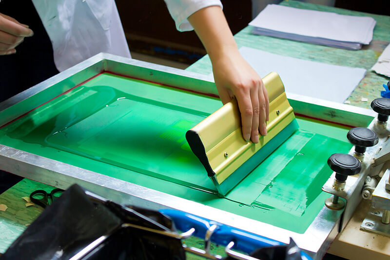
Next is solder mask. This green (or sometimes blue, red, or black) coating protects copper and keeps solder only where needed. Silk-screening then prints component labels and logos.
Electrical testing is critical. Automated probes check continuity and isolation. Any shorts or open circuits trigger rework.
Finally, the panel is cut into individual boards. Each product is cleaned, packaged, and ready to be shipped to the assembly line or directly to you.
Which PCB manufacturing steps matter most?
Every step counts, but three stand out.
Imaging and Etching: Accurate imaging ensures the circuit matches design specs.
Drilling and Plating: Proper plating guarantees strong inter-layer connections.
Testing: Rigorous electrical tests catch defects before assembly.
BEST Technology uses advanced equipment and strict quality controls during these critical stages. Automated optical inspection, clean rooms, and real-time monitoring protect consistency.
What is in a circuit board components list?
A circuit board components list, often called a bill of materials (BOM), details everything needed for assembly. It includes:
Special Parts: Sensors, antennas, or displays unique to your design.
Each item specifies part numbers, tolerances, and approved suppliers. A clean BOM speeds sourcing and lowers cost.
BEST Technology, as an experienced printed circuit board PCB manufacturers, usually helps to complete the list and recommend parts with a stable supply and better prices.
Which materials do PCB factories use?
The foundation of a PCB is the laminate. FR-4, a fiberglass-epoxy composite, remains the industry standard. It balances strength, thermal resistance, and cost.
For high-frequency or high-speed boards, BEST Technology’s factories will use materials such as Rogers or polyimide. These offer lower dielectric loss and better heat performance.
Copper foil forms the conductive layers. Thickness ranges from 0.5 oz to 3 oz per square foot depending on current needs.
Solder mask is usually epoxy-based for durability. Surface finishes like ENIG (Electroless Nickel Immersion Gold), HASL (Hot Air Solder Leveling), or OSP (Organic Solderability Preservative) protect pads from oxidation and improve soldering.
What drives PCB manufacturing cost and speed?
Several factors influence cost and lead time.
Layer Count: More layers mean more drilling, lamination, and testing.
Board Size and Quantity: Larger or thicker boards use more material and require longer machine time.
Trace Width and Spacing: Fine pitch designs demand tighter process control and raise cost.
Surface Finish: Gold plating and advanced coatings cost more than simple HASL.
Testing Level: Flying-probe or functional tests add time but ensure reliability.
To speed up production, BEST Technology, a top PCB manufacturer, uses automated production lines and intelligent scheduling. We also offer a no-minimum-order option, allowing for rapid prototyping without waiting for volume orders.
What certifications should circuit board manufacturing companies hold?
Quality certifications prove a factory follows global standards.
ISO 9001: Shows strong quality management across the entire process.
UL Certification: Ensures boards meet safety standards for flammability.
RoHS and REACH Compliance: Confirms materials are free of restricted hazardous substances.
IATF 16949: Important for automotive electronics.
ISO 13485: Required for medical device PCBs.
Working with certified circuit board manufacturers protects your product and brand reputation. We hold relevant quality certifications that validated our commitment to provide high quality products. These certificationsact as a guarantee of product excellence, ensuring customers and partners a good quality assurance practices.
How to pick the best PCB circuit board manufacturer?
Selecting the right partner means balancing technology, service, and flexibility.
Start with capability. Does the factory handle your board size, layer count, and finish? Do they support rigid-flex or HDI if you need them?
BEST Technology begin to As a printed circuit board (PCB) vendor in Asia, we are dedicated to be your best partner of advance, high-precision printed circuit boards, such as heavy copper boards, mixed layers, high TG, HDI, high frequency (Rogers, Taconic), impedance controlled board, Metal Core PCB (MCPCB) such as Aluminum PCB, Copper PCB, and so on.
Established PCB manufacturer teams know how to solve complex issues and scale from prototype to mass production.
EBest Circuit (Best Technology) provides rapid PCB prototyping services. We provide PCB prototype service with FR4 PCB, Ceramic PCB, MCPCB, HDI PCB, heavy copper PCB, High TG PCB, RF PCB and so on. Pls let us know if you have any questions about PCB.
Look for transparent communication. A reliable supplier provides clear quotes, fast technical feedback, and regular updates.
EBest Circuit (Best Technology) provides full turnkey services in China with more than 19 years of experience, We’ll respond to your inquiries 24 hours a day, providing the best services at competitive prices.
Evaluate speed and flexibility. A factory offering no MOQ lets you order small runs for testing without penalty.
Best technology No MOQ quantity requirement, even 1 piece, we can help you.
Finally, consider support. Post-delivery service and warranty show confidence in their product.
Based on our strict quality control system, we are so confident in our product that will guarantee money-back for any defective products. We will re-fabricate the boards for free or make refund with no reason. You don’t need to worry anything!
EBest Circuit (Best Technology)’s one-stop serviceβfrom design input to assemblyβcan help you quickly move from idea to market.
When you seek dependable PCB circuit board manufacturers or a PCB factory with no MOQ, choose a partner with proven experience and strong service. BEST Technology ensures your project starts on time and runs smoothly.
What is a HMI PCB? Let’s discover its components, benefits, function, purpose, application, design technique for signal integrity, optimize layout solution for HMI PCB board.
Are you troubled with these problems?
Touch response lag?
PCB overheating issues?
Poor multi-device compatibility?
As a HMI PCB manufacturer,EBest Circuit (Best Technology) can provide you service and solutions:
A HMI PCB, or Human-Machine Interface printed circuit board, is a specialized interface enabling direct interaction between users and devices like Power Wheelchairs, featuring intuitive controls for seamless operation. This HMI Board integrates tactile buttons, touchscreens, or voice commands to ensure users with diverse needs can navigate Power Wheelchairs safely and efficiently. By prioritizing accessibility and user-centric design, the HMI Board becomes an essential HMI Board in power-assisted mobility, transforming personal mobility experiences.
What Are Components of HMI PCB Board?
Components of HMI PCB Board:
Main Control MCU: Low-power microprocessor (e.g., ARM Cortex-M series) for command parsing and system scheduling.
Multi-dimensional Input Interfaces: Analog joystick signal conditioning circuit + digital key matrix + assistive device ports (eye tracker/respiration sensor).
Display Driver Unit: LCD controller + backlight circuit + LED status indicator array.
Real-time Communication Module: CAN/UART transceiver (connects to main controller) + isolated protection circuit.
Assistive Device Integration: Supports eye-tracking/voice modules for accessibility.
System Health Monitoring: Diagnoses PCB temp/voltage fluctuations with overheat protection.
What Are Advantages of HMI Board?
Intuitive & Efficient Human-Machine Interaction: Enable rapid command transmission and real-time device feedback through touchscreens, physical buttons, or hybrid inputs, reducing operational complexity and boosting productivity.
Industrial-Grade Durability: Built with high-temperature-resistant, dustproof, waterproof, and vibration-resistant materials, ensuring reliable 24/7 operation in harsh environments like manufacturing lines and outdoor equipment.
Multi-Protocol Communication Compatibility: Integrate CAN, Modbus, Ethernet, Wi-Fi, Bluetooth, and other interfaces to seamlessly connect with PLCs, sensors, and cloud platforms for device networking and remote monitoring.
Highly Integrated Functional Modules: Combine display, control, data processing, and storage into a single board, minimizing wiring complexity and space usage while enhancing system reliability and maintainability.
Customizable Interface Development: Support graphical editing tools for quick customization of industry-specific interfaces (e.g., industrial control panels, medical device screens), meeting unique user requirements.
Real-Time Data Processing & Feedback: Leverage high-performance processors and dedicated chips for real-time monitoring, fault alerts, and data visualization, optimizing decision-making and production workflows.
Energy-Efficient Design: Employ low-power chips and dynamic power management to reduce energy consumption, extend battery life, and align with green manufacturing standards.
Robust EMI/EMC Immunity: Ensure stable signal transmission and device safety through compliant designs like shielding layers and filter circuits, minimizing high-frequency noise interference in industrial settings.
Rapid Iteration & Upgrade Support: Enable modular design and OTA (Over-The-Air) updates for effortless feature expansion, firmware updates, and security patching, lowering lifecycle costs.
Cross-Platform System Compatibility: Compatible with Windows, Linux, RTOS, and other OSes, adapting to industrial PCs, embedded devices, and mobile terminals for flexible system integration.
What Are Applications of HMI Circuit BoardοΌ
Electric Wheelchair Smart Control
Industrial Robot Teach Pendants
Smart Wearable Devices
EV Charging Stations
Medical Device Control Panels
Smart Agricultural Machinery
Port Gantry Crane Remote Control
Automated Production Lines
How to Design HMI Control Board for Signal Integrity?
Signal Integrity Design Strategies for HMI Control Boards
Optimize for FR4 substrate (Tgβ₯135β) instead of high-cost polyimide, cutting material costs by 40% while meeting IEC 60068-2-1 thermal shock requirements. DSC verification confirms thermal stability for HMI applications like electric wheelchair control panels. Low-loss FR4 (Ξ΅r=4.2-4.5) maintains signal loss β€2dB/m for touchscreen high-frequency signals.
Modular Functional Partitioning
Divide HMI board into touch control, power management, and communication modules using QFP/BGA standardized packages. For electric wheelchair HMI boards, touch modules integrate capacitive touch controllers and signal conditioning circuits. Altium Designer pre-layout simulation optimizes inter-module trace length (β€5cm), reducing debugging time by 20% and achieving 99.5% SMT yield.
Manufacturing Process Precision Control
Adopt IPC-7351B standard pad dimensions (e.g., 1.0mmΓ0.5mm for 0402 packages) with lead-free soldering. AOI + flying probe testing ensures 100% open/short detection. For HMI touch interfaces with β₯0.5mm pad spacing, optimized reflow profiling (245βΒ±5β) reduces soldering defects to β€0.5%, cutting rework costs by 15%.
Enhanced Design-for-Testability (DFT)
Place β₯100mil-spaced test points on critical paths (CAN bus/IΒ²C) for ICT/flying probe testing. IEEE 1149.1 boundary scan reduces HMI board test time by 50%. Electric wheelchair examples include JTAG interfaces for rapid firmware flashing and functional verification, lowering production line testing labor costs by 30%.
Thermal-Mechanical Co-Design
ANSYS Icepak thermal simulation guides power device placement with thermal via arrays (0.3mm diameter, 1mm pitch) under processors to maintain junction temperatures β€85β. IEC 60068-2-6 compliant “grid” stiffener design improves mechanical robustness, reducing transport damage scrap rates by 20% for mobile HMI applications.
Supply Chain & Inventory Optimization
“Common components + custom modules” strategy uses mainstream ICs (e.g., STM32 series) for supply chain stability. MRP systems precisely calculate component usage, reducing inventory holding costs by 15%. Local procurement of touchscreen modules in electric wheelchair projects shortens lead times to β€5 days, lowers logistics costs by 25%, and enhances production flexibility.
Deep involvement in PCBA for 19 years with focus on HMI control board R&D, accumulating top-tier industrial process databases and failure analysis cases.
Clients inherit mature technical solutions, reducing R&D trial costs by over 30%, achieving 99%+ yield rate, and shortening time-to-market by 40%.
Free DFM Optimization for Manufacturability
Full-process free DFM analysis identifies design flaws early and optimizes layouts (e.g., component spacing, pad dimensions, thermal design).
Avoids mass production rework, cuts design change costs by 50%+, boosts first-pass yield to 98%, and saves millions in development expenses.
Rapid Delivery with 99.2% On-Time Rate
“24-hour response + 7-day extreme delivery” mechanism with intelligent production scheduling ensures 99.2% on-time delivery.
Enhances supply chain turnover by 35%, prevents million-dollar order losses from delays, and ensures precise project milestone control.
Six-Level Quality Control
Six comprehensive inspections from raw materials to finished products (e.g., AOI, X-RAY, functional testing).
Achieves <0.05% defect rate, reduces after-sales costs by 80%+, raises end-user satisfaction to 98%, and strengthens brand reputation.
Dedicated HMI Production Line & Custom Capability
HMI-specific SMT line with core technologies (high-density wiring, microvia filling, high-temp solder).
Supports complex designs (touch + display integration, anti-interference circuits), outperforms industry by 15%, and meets premium market demands.
Full-Chain After-Sales & Lifetime Tech Support
7Γ24 technical support with 48-hour on-site resolution and free documentation updates.
Ensures worry-free usage, cuts O&M costs by 30%, extends product lifecycle, and boosts loyalty/repurchase rates.
Modular Platform & Rapid Iteration
Standardized module library (display, button, power modules) enables rapid assembly and functional expansion.
Increases iteration speed by 50%, supports small-batch multi-variety production, meets customized needs, and captures market opportunities.
Transparent Traceability & Data-Driven Management
MES system enables full-process data visualization and traceability from raw materials to finished products.
What is copper coin PCB? Let’s explore its benefits, applications, technical spec, cost reduction solution, production process and market analysis for copper coin PCB.
Are you worried about these problems?
Is your electronics product throttling due to inadequate heat dissipation, causing performance loss?
Are traditional PCB cooling solutions eating into your profit margins with skyrocketing costs?
Does complex multi-layer stacking design keep your product yield below 90%?
As a copper coin PCB manufacturer, EBest Circuit (Best Technology) can provide you service and solution:
Embedded copper coins slash thermal resistance by 60%, run devices at full power, no derating.
Integrated heat dissipation design eliminates extra cooling modules, cutting total costs by 25%.
Standardized copper coin insertion process boosts yield to 95% and shortens lead time by 30%.
Copper Coin PCBis a specialized design that embeds solid copper blocks (copper coins) into multi-layer printed circuit boards. These copper coins directly connect heat-generating components to external heat sinks, creating high-efficiency thermal paths. Features include copper coin placement under high-power devices (in shapes like circles, rectangles, or stepped designs) to maximize contact area, boosting thermal dissipation efficiency by up to 55x compared to traditional methods like thermal vias or heat sinks.
Advantages of PCB Copper Coin
Benefits of copper coin PCB:
High Thermal Conductivity: Copper’s excellent heat dissipation properties rapidly transfer heat away from components, reducing device operating temperatures and enhancing stability and longevity.
High Current Carrying Capacity: Thick copper layers or coin-shaped structures enable higher current handling, minimizing resistive losses for high-power applications.
Enhanced Mechanical Durability: Copper coin designs strengthen PCB resistance to vibration and impact, reducing physical damage risks during transport or use.
Cost Efficiency: Optimized copper layout reduces precious metal usage or replaces external heat sinks, lowering overall manufacturing costs.
Simplified Design Process: Integrated heat dissipation and current pathways eliminate the need for external cooling modules, shortening development cycles and streamlining assembly.
Applications of Copper Coin- Embedded PCB
Aerospace & Space Exploration: Core modules of onboard computers in satellites, Mars rovers, and other space equipment.
5G Base Stations & RF Modules: Power amplifiers (PA) and RF front-end modules in 5G base stations.
Electric Vehicles & Power Control: Motor controllers, battery management systems (BMS), and IGBT modules in electric vehicles.
High-Performance Computing & Servers: High-performance computing (HPC) modules, GPU accelerators, and CPU/GPU thermal management modules in data centers.
Industrial Control & Frequency Converters: Industrial PLCs, frequency inverters, and variable-frequency drives.
Miniature Medical & Wearable Devices: Cardiac pacemakers, implantable medical devices, smartwatches, and other compact electronic devices.
Copper Coin PCB Technical Specifications
Parameter Category
Detailed Specifications
Substrate Material
FR4 (Tg170), Rogers RO4350B, Aluminum-composite
Copper Layer Thickness
1-10 oz (35-350ΞΌm)
Copper Coin Structure
Diameter 0.3-10mm, Height 0.2-5mm, embeddable in single/multilayer PCB
Design Rule Checks: Use tools like Cadence DRC/DFM to flag costly errors (acid traps, starved thermals) pre-fabrication.
Manufacturer Collaboration: Validate design choices with fabricators to align with their capabilities and cost structures.
Copper Coin PCB Production Process
1. Copper Coin PCB Production Process
Operations: Cutting large-size copper-clad laminate into production panels, edge grinding, rounding, washing, and baking (dry treatment).
Parameters: Edge reserved 8-15mm for process margin; dimensions adjusted for equipment compatibility (e.g., 3Γ3 matrix panels from 41Γ49 inch sheets).
2. Inner Layer Circuit Production
Pre-treatment: Brush/sandblast to remove copper oxidation and oil, enhancing adhesion.
Photoresist Application: Coat liquid/dry film, cure at 80Β°C.
Exposure & Development: Transfer pattern via UV exposure, develop with NaβCOβ to expose copper for etching.
Packaging: Cleaned, dried, vacuum-packed/moisture-barrier bags with inspection reports and labels.
Copper Coin PCB Market Trends Analysis in 2025
Accelerated Technology Standardization
IPC will release the IPC-7095D standard in Q2 2025, specifying embedded copper coin tolerances (Β±0.05mm) and thermal cycling test protocols.
Industry yield rate rises from 85% (2023) to 92%, reducing SMEs’ design cycles by 30%.
NEV Emerges as Primary Growth Market
Global EV production will hit 28 million units (DIGITIMES 2024), with >52% adoption of SiC MOSFETs in powertrains (operating >150β).
Automotive-grade Copper Coin PCB demand surges 40%, priced 3.8Γ higher than standard FR-4 PCBs.
Hybrid Substrate Solutions Gain Traction
Copper-Aluminum Nitride (AlN) substrates achieve 650W/mΒ·K thermal conductivity (96% CTE match), with costs dropping 25% due to mass production.
Penetration in data center GPU thermal modules reaches 38% (vs. 12% in 2023).
Regional Supply Chain Restructuring
North American players (TTM/Ventec) dominate aerospace (55% share), but China’s “New Infrastructure” policy boosts local players like SCC (share up from 19% to 28%).
Geopolitical tensions drive copper raw material price volatility (Β±18%).
Environmental Regulations Drive Tech Innovation
Revised EU WEEE Directive (2025) mandates β₯90% PCB copper recovery, increasing chemical etching waste treatment costs to $85/ton.
Laser etching investments grow 200%, reducing copper waste by 12%.
No, a MOSFET is an individual transistor that can switch or amplify electrical signals, while CMOS is a technology that combines complementary MOSFETsβboth N-channel and P-channelβto create highly efficient digital circuits. One is a building block, and the other is a design method that uses thousands or even billions of those blocks. To really see the difference, letβs walk through what each term means and how they connect in todayβs electronics.
What is a MOSFET?
A MOSFET stands for Metal-Oxide-Semiconductor Field-Effect Transistor. It is one of the most widely used electronic components in the world. Think of it as a tiny switch that can turn current on and off in a circuit. Unlike older switches that rely on mechanical movement, MOSFETs work by using an electric field to control the flow of charge. This makes them fast, efficient, and durable.
MOSFETs appear in everything from power regulators to memory chips. They can handle both high power and delicate signal processing, which is why they are everywhere in modern electronics. Because they are scalable and reliable, engineers continue to rely on MOSFETs as the backbone of both analog and digital systems.
Does A MOSFET is Composed of Four Elements?
Every MOSFET has four terminals, and each one has a unique role:
Source β This is where the current carriers, usually electrons or holes, enter the device.
Drain β This is where the carriers leave the device after passing through the channel.
Gate β This is the control terminal. By applying a voltage here, you decide whether the channel between source and drain is open or closed.
Body (or Substrate) β This is the underlying layer of material that holds the structure together. It usually connects to a fixed potential to stabilize the device.
Together, these four parts make the MOSFET function like a controlled valve. Imagine turning a faucet on and off with your hand. The gate in a MOSFET does the same job, but it uses voltage instead of physical effort.
Types of MOSFET
MOSFETs are classified based on their channel type, conduction mode, and power handling. Choosing the right type depends on the application. Hereβs a detailed overview:
N-Channel MOSFET
Uses electrons as majority carriers.
Requires a positive voltage at the gate relative to the source to turn on.
Often used for low-side switching, where the source connects to ground.
Advantages: High electron mobility allows faster switching and higher efficiency.
P-Channel MOSFET
Uses holes as majority carriers.
Requires a negative gate voltage relative to the source to turn on.
Commonly used for high-side switching, where the source connects to the positive supply.
Slightly slower than N-channel MOSFETs due to lower hole mobility.
Enhancement Mode MOSFET
Normally off when the gate-source voltage is zero.
Requires a gate voltage to enhance conductivity.
Most modern MOSFETs are enhancement mode, especially in digital circuits and power applications.
Depletion Mode MOSFET
Normally on at zero gate voltage.
Applying a gate voltage reduces conductivity.
Less common but useful in some analog circuits.
Power MOSFET
Designed to handle high currents and voltages.
Often used in power electronics, such as inverters, motor drives, and LED drivers.
Features low on-resistance to reduce power loss.
Why MOSFETs are Important in Power Electronics?
We can say, MOSFETs are the backbone of modern power electronics. Their role goes far beyond simple switchingβthey determine efficiency, thermal performance, and the reliability of electronic systems. Hereβs why they are indispensable:
High Switching Speed
MOSFETs can turn on and off in nanoseconds. This rapid switching is crucial for high-frequency applications such as DC-DC converters, switch-mode power supplies, and motor drivers. Faster switching reduces energy loss in the form of heat, enabling compact designs and higher efficiency.
Unlike bipolar transistors, MOSFETs require almost no current to control the gate. A small voltage is enough to switch large currents on and off. This allows microcontrollers and digital circuits to drive MOSFETs directly without additional amplifiers, simplifying the circuit design.
High Current and Voltage Handling
Power MOSFETs can manage high currents (tens or hundreds of amps) and high voltages (up to thousands of volts). This capability makes them ideal for industrial inverters, electric vehicle motor controllers, and LED drivers. Designers can achieve higher power density without sacrificing reliability.
What is CMOS?
CMOS stands for Complementary Metal-Oxide-Semiconductor. Instead of being a single component, CMOS refers to a technology for building logic circuits. It combines two types of MOSFETs:
NMOS (n-type MOSFETs) β These conduct when a positive voltage is applied to the gate.
PMOS (p-type MOSFETs) β These conduct when a negative voltage is applied to the gate.
By using both NMOS and PMOS in pairs, CMOS circuits achieve something very valuable: low power consumption. A CMOS gate only draws significant current when it switches states. In steady operation, it hardly wastes any energy. This is why CMOS has become the standard for digital electronics. From smartphones to cloud servers, CMOS technology powers almost every digital device you know.
What is the Difference Between a CMOS and a MOSFET?
The distinction is clear once you see their roles:
A MOSFET is a transistor, a single device used to switch or amplify signals.
CMOS is a circuit design method that arranges MOSFETs in complementary pairs to create logic gates and larger systems.
Feature
MOSFET
CMOS
Definition
A single transistor used for switching or amplification
A circuit technology using pairs of MOSFETs (NMOS + PMOS)
Level
Device level (individual component)
Circuit/system level (logic gates, processors)
Power Consumption
Depends on usage; can consume more when switching
Very low static power; only draws current during switching
Usage
Power electronics, amplifiers, signal processing, regulators
Digital logic circuits, CPUs, memory, sensors
Scalability
Used alone or in small groups
Scales to billions of transistors in integrated circuits
Example
Voltage regulator in a laptop charger
Processor inside a laptop or smartphone
In simpler words, MOSFETs are the bricks, and CMOS is the architectural style that uses those bricks to build skyscrapers. Without MOSFETs, CMOS would not exist. But a single MOSFET by itself is not CMOS.
Does CMOS Use MOSFETs?
Yes, absolutely. CMOS is built entirely from MOSFETs. Each logic gateβwhether itβs an inverter, AND, or OR gateβuses a pair of MOSFETs working together. One MOSFET pulls the output high, while the other pulls it low. Because only one of them conducts at a time in steady states, the circuit hardly consumes static power.
This is why CMOS chips run cool compared to older technologies like TTL (Transistor-Transistor Logic). It is also the reason why CMOS scaled so well into modern processors and memory chips. Without the efficiency of MOSFETs, todayβs electronic devices would overheat or drain batteries far too quickly.
Do Modern CPUs Use MOSFETs?
Yes, and not just a few of them. Modern CPUs contain billions of MOSFETs, all arranged in CMOS configurations. Each transistor acts as a tiny switch, controlling whether a bit of information is a β0β or a β1.β
As manufacturing processes advanced, engineers learned to shrink MOSFETs to nanometer sizes. Today, CPUs use MOSFETs that are only a few dozen atoms wide. This scaling has allowed CPUs to pack more power into smaller chips while keeping energy use under control.
For example, a high-end processor from a decade ago may have had a few hundred million transistors. Today, advanced CPUs in smartphones and servers have tens of billions of MOSFETs, all functioning in harmony thanks to CMOS technology.
Why Do People Confuse MOSFETs and CMOS?
The confusion comes from the overlap in terminology. Since CMOS circuits are built from MOSFETs, people sometimes use the terms loosely. However, the key difference is scope. A MOSFET is an individual transistor. CMOS refers to an entire circuit style that depends on using many MOSFETs in complementary pairs.
Itβs a bit like confusing a single letter with a whole alphabet system. The letter is part of the system, but not the same thing as the system itself.
Conclusion
So, are MOSFETs and CMOS the same? No, they are not. MOSFETs are individual transistors, while CMOS is a circuit design style that relies on MOSFET pairs. One provides the building blocks, and the other organizes them into powerful digital systems.
At EBest Circuit (Best Technology), we understand how critical both MOSFETs and CMOS are in modern circuit design. Our PCB manufacturing services support advanced semiconductor packaging and power management needs. With certifications like ISO9001, ISO13485, IATF16949, and AS9100D, we deliver boards trusted by industries from medical to aerospace. Using MES systems, we guarantee full traceability and rigorous quality control.
If you are designing circuits that involve MOSFETs, CMOS, or advanced digital logic, EBest Circuit (Best Technology) is here to provide the PCB solutions you need with precision, reliability, and competitive pricing.
FAQs
1. Why are MOSFETs important in electronics?
MOSFETs act as fast switches that control current with very little power. This makes them ideal for both power and signal applications.
2. Why is CMOS more efficient than other logic technologies?
Because only one transistor in a CMOS pair conducts at a time, it consumes very little power in a steady state.
3. Can you have CMOS without MOSFETs?
No. CMOS is entirely built from MOSFETs. Without them, CMOS circuits would not exist.
4. How many MOSFETs are in a CPU?
Modern CPUs can contain billions of MOSFETs, each working as a tiny on/off switch to perform logic operations.
5. Are MOSFETs used only in digital circuits?
No. MOSFETs are also widely used in analog circuits, power supplies, amplifiers, and motor controllers.
The single throw double pole switch PCB is an essential component in modern electronics, offering a reliable way to control two independent circuits simultaneously with a single action. The points of this blog revolve around the key aspects of Single Throw Double Pole (DPST) Switch PCBs, including their definition, core features, different types, practical applications, working principle on PCBs, selection guidelines, wiring diagrams, and others.
Insertion loss, return loss, and isolation parameters do not meet expectations, resulting in unstable performance?
Mechanical structure and materials affect long-term reliability, and lack environmental adaptability?
Lack of sufficient customization options to meet specific needs?
Difficult for validation, since high-frequency switch testing requires complex equipment and methods?
EBest Circuit (Best Technology) gives viable solutions as follows.
Optimized design and material selection.
Provide customized switch designs according to customer requirements, including dimensions, packaging, and interfaces.
Offer technical support and testing services.
Optimize supply chain management, shorten lead times, and ensure customers receive products on schedule.
Establish a strict quality control system to ensure products meet customer requirements.
As a established PCB and SMT factory, EBest Circuit (Best Technology) gives full engagement including single throw double pole switch PCBprototypes, material procurement, fabrication, assembly SMT, and box build service. All material we used are fully compatible with ISO 9001, ISO 13485, IATF 16949, AS9100D, UL, REACH, and RoHS. Our engineers provide full support from design to mass production, ensuring short lead times and faster market entry. If you interested in our PCB services, pls email us at sales@bestpcbs.com.
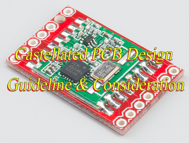
What is Single Throw Double Pole Switch PCB?
βPole (P):ββ The number of βcompletely separate, electrically isolated circuitsβ that the switch can control simultaneously.
βThrow (T):ββ The number of βdifferent output connectionsβ that each pole’s common terminal can be connected to.
Single Throw Double Pole Switch PCB: A printed circuit board (PCB) that integrates a switch component with two independent circuits (double pole) and only one switching position per circuit (single throw).
Functional Definitions of the Three Switches
1. Single Pole, Single Throw (SPST)
This is the most fundamental form of a switch, providing binary operation.
βStructure:ββ It consists of βone set of contactsβ (one movable contact and one stationary contact).
βFunction:ββ Its sole purpose is to βopenβ or βcloseβ a single electrical path. It has two states: βON (closed)ββ or βOFF (open)β.
βApplication:ββ Used for basic power switchingβturning a circuit completely on or off (e.g., a power kill switch, a simple light circuit).
2. Single Pole, Double Throw (SPDT)
This switch adds the function of βpath selectionβ or βsignal routing.
βStructure:ββ It has βone common movable contactβ and βtwo stationary contacts. The common contact can be connected to either one of the two stationary contacts.
βFunction:ββ Routes one input circuit between two output paths. It connects a common terminal (COM) to either Terminal A or Terminal B. It typically has three states: βConnect to A, Open (center-off), Connect to B.
COM ↔ Terminal A COM ↔ Terminal B (Note: Some SPDT switches include a center-off position where COM is disconnected from both A and B.)
βApplication:ββ Used for selecting between two sources or paths (e.g., switching an audio amplifier’s input between a CD player and a radio tuner, selecting a device’s operating mode).
3. Double Pole, Double Throw (DPDT)
This is a compound switch enabling βsynchronous control of two independent circuits.
βStructure:ββ It contains βtwo independent sets of SPDT contacts. The switching mechanisms for both sets are βmechanically linkedβ and operated by a single actuator. Each side of a DPDT switch functions like an individual SPDT switch, so it can effectively be used as two SPDT switches. K2 is a Double Pole Double Throw (DPDT) switch, while K1 and K3 are Single Pole Double Throw (SPDT) switches.
βFunction:ββ It simultaneously switches the operating states of two independent circuits. It can synchronously change Circuit 1 and Circuit 2 from one connection mode (e.g., A1βA2) to another mode (e.g., B1βB2).
βApplication:ββ
βMotor control:ββ Reversing the direction of a DC motor by swapping the polarity of the power connection to its terminals.
βSignal routing:ββ Switching a stereo audio signal, routing both the left and right channels to different destinations simultaneously.
Feature
SPST PCB
SPDT PCB
DPDT PCB
βCore Functionβ
Make or Break a circuit
Select between two paths
Synchronous switching of two circuits
βPrimary Actionβ
On/Off
Changeover
Polarity Reversal / Complex Switching
βKey Differentiatorβ
Basic switching
Adds βselectionβ
Adds βsynchronous controlβ
In essence:
Use a βDPDTβ PCB when you need to βcontrol the state of two circuits at onceβ in a coordinated manner.
Use an βSPSTβ PCB when you only need to βconnect or disconnectβ a circuit.
Use an βSPDTβ PCB when you need to βchoose between two pathsβ for a single circuit.
What are the Features of Single Throw Double Pole Switch PCB?
From a design and application perspective, a high-quality DPST switch PCB offers the following five core characteristics:
1. Synchronous Dual-Channel On/Off Control Essential Feature: With a single mechanical action, it synchronously controls two completely independent circuits to turn on or off at the same time. This is the fundamental difference compared with SPST (Single Pole Single Throw) and SPDT (Single Pole Double Throw) switches.
3. Robust PCB-Integrated Structure Mechanical Feature: The switch body is soldered directly onto the PCB through multiple pins, offering superior structural strength, vibration resistance, and fatigue durability compared with wire connections. The PCB serves as the base, providing resistance to torque and lateral stress, ensuring that pads remain intact even under frequent operation.
4. Excellent Current-Carrying and Voltage Endurance Performance Electrical Parameters: The contact material (such as silver alloy) and structural design determine the rated current (e.g., 10A/125VAC, 5A/250VAC) and rated voltage. The copper trace width on the PCB must be matched accordingly to avoid thermal bottlenecks across the entire conduction path.
5. Standardized Packaging for Automated Production Manufacturing Advantage: To support SMT or wave soldering processes, DPST switches typically adopt standardized pin spacing (e.g., 5.08mm, 7.62mm) and package dimensions. PCB layouts must strictly follow the recommended pad pattern and thermal profile for reflow soldering to maintain high yield.
All in all, a DPST switch PCB is not a simple on-off component. It is a mechatronic module optimized for high reliability and safety in dual-channel synchronous power control. Its characteristics revolve around five key dimensions: synchronization, isolation, robustness, high power handling, and manufacturability.
What are the Types of DPST Switch?
DPST (Double Pole Single Throw) switches are available in various forms to meet different functional and design requirements. Each type can be adapted for PCB mounting, which helps engineers maintain a clean layout and reduce wiring errors. The main types include:
1. Mechanical DPST Switch Mechanical DPST switches are the most common type. They operate by physically opening and closing circuits through a mechanical structure. Typically, they feature a lever, knob, or toggle actuator. Rotating or pressing the actuator moves the internal contacts to connect or disconnect the circuits. This type is robust, reliable, and widely used in industrial or power applications.
2. Electronic DPST Switch Electronic DPST switches represent a modern approach. Instead of mechanical contacts, they use semiconductor devices to control circuit switching. The operation is often via a button, touchscreen, or other electronic interface. This type offers faster response times, precise control, and enhanced durability, making it ideal for signal detection, automation, or safety-critical applications.
3. Common Form Factors of DPST Switches
Push Button DPST Switch: Activated by pressing, suitable for reset functions or manual control.
Toggle DPST Switch: Simple lever operation, commonly used for power mode selection.
Slide DPST Switch: Compact sliding action, ideal for small electronics or dual-mode devices.
Rocker DPST Switch: Ergonomic design, suitable for frequent on/off applications.
Micro DPST Switch: High-precision, small footprint, excellent for signal detection and safety features.
Each form factor can be selected based on application requirements, PCB layout constraints, and desired user interaction.
What are the Usage of Single Throw Double Pole Switch PCB in PCB?
DPST (Double Pole Single Throw) switches are versatile components widely used in PCB design. Their ability to simultaneously control two independent circuits makes them ideal for multiple practical applications:
1. Power Control DPST switches can disconnect both positive and negative lines at the same time, providing enhanced safety for electronic devices and reducing the risk of accidental shorts.
2. Signal Switching They are well-suited for audio, communication, and control circuits that require simultaneous dual-path switching. This ensures consistent signal routing and minimizes signal interference.
3. Mode Selection DPST switches can toggle between two operation modes of a device with a single action. This simplifies user interaction and reduces the number of components required for mode control.
4. Circuit Protection By controlling two circuits together, DPST switches help prevent accidental overloads or short circuits. This adds an extra layer of protection to sensitive electronics.
Integrating DPST switches directly onto PCBs helps reduce wiring complexity, improve layout cleanliness, and enhance overall system reliability. This addresses common customer concerns about circuit failures, maintenance difficulties, and assembly errors.
DPST switches are widely applied across various electrical devices and systems:
Home Appliances: Control of lights, sockets, and other household devices.
Industrial Equipment: Control and protection of machines and production systems.
Power Systems: Switching and protection of electrical circuits in power distribution networks.
By combining dual-circuit control with PCB integration, DPST switches offer both operational efficiency and enhanced safety across multiple sectors.
How Does a Single Throw Double Pole Switch Work on a PCB?
A DPST switch controls two independent circuits simultaneously through a single actuator. It operates in two basic states:
Open (Off) State: In this state, the moving contacts are separated from the fixed contacts, and no current flows between the two terminals. The circuit is effectively disconnected.
Closed (On) State: When the switch is actuated, the moving contacts make firm contact with the fixed contacts, completing the circuit and allowing current to flow.
The actuatorβcommonly a lever, knob, or toggleβmoves the contacts from one position to another, enabling simultaneous switching of both circuits. This dual-path control ensures consistent operation for applications requiring synchronized circuit management.
How It Connects and Operates on a PCB? When integrated on a PCB, the DPST switch is typically soldered directly onto designated pads via multiple pins. This setup provides several key benefits:
Mechanical Stability: The PCB acts as a solid base, supporting the switch against torque and lateral forces. This prevents loosening or pad damage, even under frequent switching.
Electrical Reliability: Each pole connects to PCB copper traces sized according to the switchβs rated current and voltage. Proper trace width ensures safe current flow and prevents overheating.
Operational Simplicity: Users actuate the switch through its handle or lever, which moves both poles simultaneously. The PCB layout guarantees clean routing for both circuits, minimizing cross-talk and interference.
Advantages of Integrating a DPST Switch Directly on a PCB Choosing PCB-mounted DPST switches instead of traditional wire-based connections provides multiple advantages:
Reduced Wiring Complexity: Direct soldering eliminates the need for extra wires, reducing assembly errors and cluttered layouts.
Enhanced Safety and Reliability: With a DPST switch controlling two circuits simultaneously, power lines can be fully isolated, improving overall system safety.
Ease of Maintenance: Fewer discrete connections mean lower chances of loose connections or accidental shorts. Troubleshooting becomes faster and more straightforward.
Support for Automated Manufacturing: Standardized pin spacing and pad layouts allow seamless integration with SMT and wave soldering processes, ensuring consistent quality and high production yield.
To sum up, on a PCB, a DPST switch is more than a simple on-off component. Its dual-circuit control, robust PCB integration, and standardized design make it a reliable and safe solution for applications that require synchronized operation of two independent circuits.
How to Select the Right DPST Switch for Your PCB Project?
For engineers and procurement specialists, selecting the correct DPST (Double Pole Single Throw) switch is a critical decision that impacts product safety, reliability, and manufacturability. This guide provides a focused, actionable framework for evaluation.
1. Define Electrical Requirements
βVoltage/Current Rating:ββ
βAC/DC:ββ Specify whether your application is AC or DC. The switch’s rated voltage and current βmust exceedβ the system’s maximum operating values.
βLoad Type:ββ This is critical. βDerate heavily for inductive loadsβ (e.g., motors, relays). A switch rated for 5A resistive load may only be suitable for a 1-2A inductive load due to inrush currents.
βThrough-Hole (THT):ββ Provides superior mechanical strength and solder joint reliability. βPreferred for most applications.ββ
βSurface-Mount (SMD):ββ Saves board space but requires careful inspection of mechanical stability, especially under repeated actuation.
βTerminal Pitch & Footprint:ββ Ensure the pin spacing (e.g., 5.08mm, 7.62mm) and overall footprint βexactly matchβ your PCB layout. Always use the manufacturer’s recommended land pattern.
βActuator Type:ββ Choose (Toggle, Rocker, Pushbutton) based on human-machine interface (HMI) design, panel cutout, and user experience requirements.
3. Evaluate Reliability and Lifetime
βElectrical Life (Cycle Life):ββ This is the key metric. Ignore mechanical life. Check the datasheet for the number of cycles βat your specific rated loadβ (e.g., “10,000 cycles at 5A/250VAC”).
βContact Material:ββ βSilver Alloyβ contacts (e.g., AgSnOβ, AgCdO) offer superior resistance to arcing and welding compared to pure silver, especially for inductive loads.
βHousing Material:ββ Must be made of βhigh-temperature, flame-retardantβ plastic (e.g., PBT, PA66 rated UL 94V-0).
4. Verify Environmental Compliance and Certifications
βIP Rating:ββ Determine the required level of ingress protection (e.g., IP67 for dust and water resistance) based on the operating environment.
βSafety Certifications:ββ βMandatory.ββ The switch must carry the required certifications for your target market (e.g., βUL/cUL, TUV, CE, CQC). Do not proceed without this.
Actionable Selection Checklist
Parameter
Key Question / Action
βLoad Typeβ
βIs my load resistive or inductive?ββ (If inductive, derate current rating significantly).
βRatingsβ
βAre the voltage/current ratings above my max operating values?ββ (Confirm for both AC and DC).
βSafetyβ
βDoes the dielectric strength meet my safety isolation requirements?ββ (Check >1500VAC).
βCertificationsβ
βDoes it have the necessary end-product safety certifications?ββ (UL, CE, etc.)
βFootprintβ
βDoes the pin pitch match my PCB layout?ββ (Verify with manufacturer’s drawing).
βMountingβ
βIs through-hole or SMD better for my assembly process and reliability needs?ββ
βEnvironmentβ
βWhat IP rating do I need for my product’s operating environment?ββ
βSamplesβ
βHAVE I ORDERED SAMPLES TO TEST FIT, FEEL, AND FUNCTION?ββ
βFinal Expert Advice:ββ
βAlways get samples.ββ Physically test the switch in your actual application circuit and environment.
βEngage supplier FAEs early.ββ Provide them with your exact application details (voltage, current, load type) for tailored recommendations.
βSpecify clearly on your BOM.ββ Beyond the part number, add descriptors (e.g., “DPST, 5A/250VAC, Toggle, THT, UL Listed”) to prevent procurement errors.
Wiring and Diagrams for DPST Switches on PCB
A DPST (Double Pole Single Throw) switch is essentially two independent SPST switches mechanically linked to operate simultaneously with a single actuator.
CRITICAL: Always verify pinout with manufacturer datasheet! Below shows the most common configuration.
Pin #
Terminal Name
Function
1
NO1 (Normally Open 1)
Output for first circuit
2
COM1 (Common 1)
Input for first circuit
3
NO2 (Normally Open 2)
Output for second circuit
4
COM2 (Common 2)
Input for second circuit
Operation: When switch is actuated, COM1 connects to NO1 simultaneously with COM2 connecting to NO2.
1. Essential Wiring Diagrams
Application 1: Safety Power Disconnect (Line/Neutral Switching)
Added mechanical mounting holes with proper keepout zones
Derated current handling for inductive loads (50-70% of nominal rating)
Included snubber circuits for motor/relay loads
Silkscreen includes pin labels and ON/OFF indicators
Performed 1:1 print verification of component placement
4. Pro Tips from the Field
Reliability Enhancement: Apply silicone conformal coating around switch base to prevent dust ingress in high-cycle applications
Thermal Management: For high-current applications (>5A), connect multiple vias to internal ground planes under COM/NO pads
Safety First: Always implement redundant isolation methods (slot cuts, guard traces) when switching mains voltage
How Does a DP Switch Work?
A Double Pole Single Throw (DPST) switch operates based on the following principles and states:
1. Open Circuit State (Off Position)
When the DPST switch is in the open circuit state, the moving contacts are separated from the fixed contacts. There is no electrical path between the two terminal pairs, preventing current flow through either circuit. Current can only pass through the switch when the operating mechanism is activated to transition it to the closed state.
2. Closed Circuit State (On Position)
When the DPST switch is in the closed state, the moving contacts make physical and electrical contact with the fixed contacts. This creates a complete conductive path between both pairs of terminals, allowing current to flow simultaneously through both independent circuits.
3. Switching Operation
The DPST switch features an operating mechanism, typically a toggle lever, rocker, or rotary knob. When this actuator is manipulated, it mechanically moves both contact poles simultaneously from their open positions to closed positions (or vice-versa). This synchronized action ensures both circuits are switched concurrently, maintaining identical states in both paths at all times.
The key operational characteristic is that both poles are mechanically linked to operate in unison with a single control action, providing simultaneous make-or-break operation for two separate circuits.
In summaryβ, the single throw double pole switch PCB is an indispensable component for safe, reliable, and efficient circuit control. The blog aims to provide engineers and designers with a comprehensive understanding of DPST PCB, helping them make informed decisions when integrating these switches’ PCB into their projects. If you need any PCBs, just feel free to reach out to us at sales@bestpcbs.com.
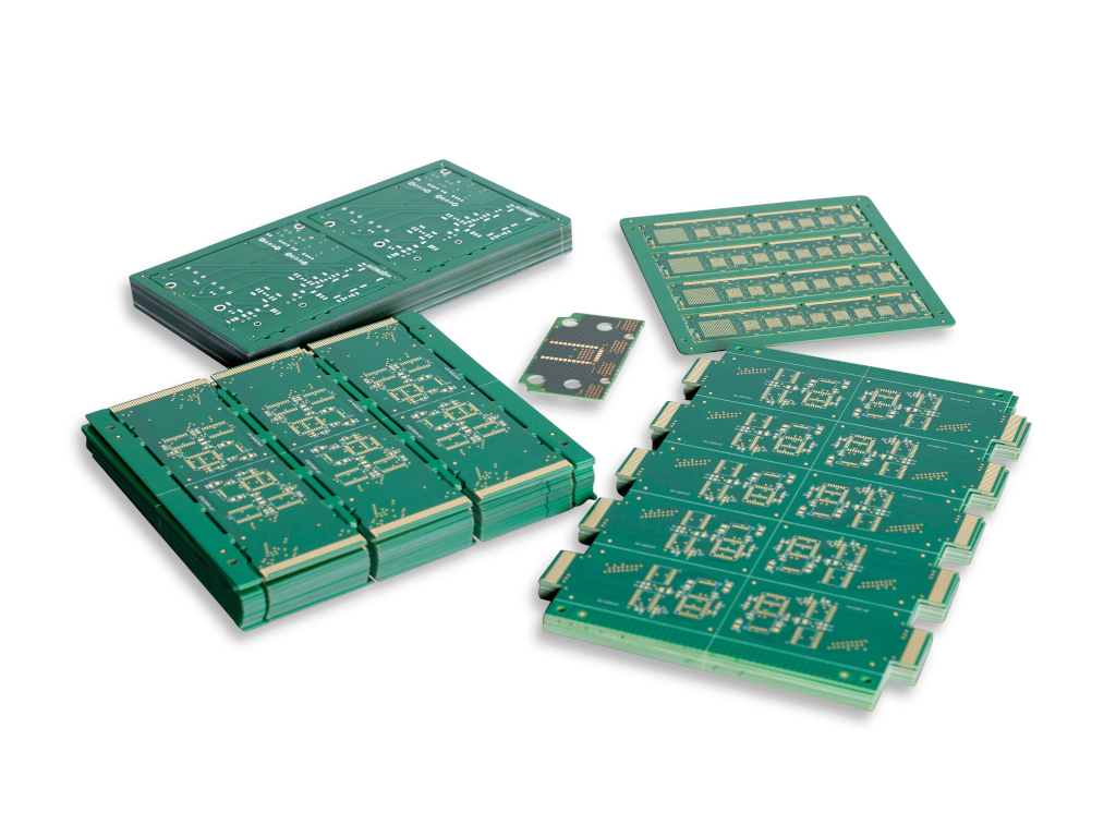
FAQs
1. Whatβs the difference between SPDT and DPDT?
SPDT (Single Pole Double Throw): Controls one circuit and can connect a single input to one of two outputs (e.g., input C β output D1 or D2).
DPDT (Double Pole Double Throw): Controls two independent circuits simultaneously. Each pole works like an SPDT switch, so it can switch two inputs at the same time (e.g., input A1βA2 and input B1βB2). Each circuit has two destination options (double throw), and the switching of the two circuits is mechanically linked and synchronized. Essentially, a DPDT is like two SPDT switches operated together.
2. Can a DPDT be used as an SPDT?
Yes. A DPDT switch can act as an SPDT by using only one of its two poles. The other pole can remain unused or be connected to perform a separate function. This makes DPDT switches versatile in applications where either single or dual circuit switching is needed.
3. What are the four types of switches?
Switches are generally categorized based on pole and throw:
SPST (Single Pole Single Throw) β Simple ON/OFF switch for a single circuit (e.g., AβB).
SPDT (Single Pole Double Throw) β Switches one input between two outputs (e.g., CβD1 or D2).
DPST (Double Pole Single Throw) β Switches two independent circuits simultaneously ON or OFF (e.g., A1βB1, A2βB2). A1βB1 represents the first circuit: when closed, current flows from A1 to B1. A2βB2 represents the second circuit: when closed, current flows from A2 to B2.
DPDT (Double Pole Double Throw) β Switches two independent circuits between two sets of outputs simultaneously (e.g., A1βA2 and B1βB2). For example: Previously: The upper path leads to A1, and the lower path leads to A2. Afterward: They simultaneously change to the upper path leading to B1 and the lower path leading to B2. To conclude, each path has two destination options (double throw), and the switching of the two paths is mechanically linked and synchronized.
This website uses cookies to enhance your experience, remember your preferences, and help us understand how visitors use our site. You can accept all cookies, reject non-essential cookies, or manage your settings.
This website uses cookies to improve your experience while you navigate through the website. Out of these cookies, the cookies that are categorized as necessary are stored on your browser as they are essential for the working of basic functionalities of the website. We also use third-party cookies that help us analyze and understand how you use this website. These cookies will be stored in your browser only with your consent. You also have the option to opt-out of these cookies. But opting out of some of these cookies may have an effect on your browsing experience.
Necessary cookies are absolutely essential for the website to function properly. These cookies ensure basic functionalities and security features of the website, anonymously.
Cookie
Duration
Description
cookielawinfo-checkbox-analytics
11 months
This cookie is set by GDPR Cookie Consent plugin. The cookie is used to store the user consent for the cookies in the category "Analytics".
cookielawinfo-checkbox-functional
11 months
The cookie is set by GDPR cookie consent to record the user consent for the cookies in the category "Functional".
cookielawinfo-checkbox-necessary
11 months
This cookie is set by GDPR Cookie Consent plugin. The cookies is used to store the user consent for the cookies in the category "Necessary".
cookielawinfo-checkbox-others
11 months
This cookie is set by GDPR Cookie Consent plugin. The cookie is used to store the user consent for the cookies in the category "Other.
cookielawinfo-checkbox-performance
11 months
This cookie is set by GDPR Cookie Consent plugin. The cookie is used to store the user consent for the cookies in the category "Performance".
viewed_cookie_policy
11 months
The cookie is set by the GDPR Cookie Consent plugin and is used to store whether or not user has consented to the use of cookies. It does not store any personal data.
Functional cookies help to perform certain functionalities like sharing the content of the website on social media platforms, collect feedbacks, and other third-party features.
Performance cookies are used to understand and analyze the key performance indexes of the website which helps in delivering a better user experience for the visitors.
Analytical cookies are used to understand how visitors interact with the website. These cookies help provide information on metrics the number of visitors, bounce rate, traffic source, etc.
Advertisement cookies are used to provide visitors with relevant ads and marketing campaigns. These cookies track visitors across websites and collect information to provide customized ads.