PCB manufacturing PCB manufacturing
Home > Blog

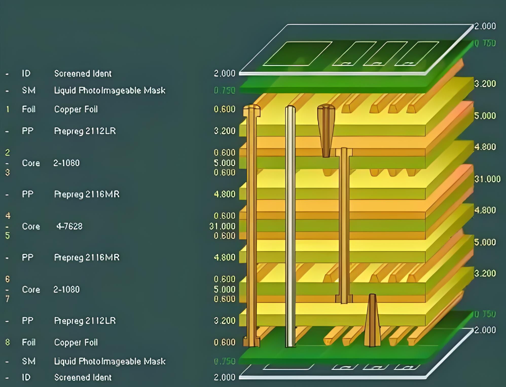
8-layer pcb stackup

PCB Board Stackup Explained: Which Layer Structure Is Right for Your Design?
Friday, July 17th, 2026

A PCB board stackup defines how copper and dielectric layers are arranged inside a printed circuit board. It determines where signals, ground references, and power distribution are placed, while also affecting impedance, EMI performance, board thickness, and fabrication cost.

Choosing a stackup is not simply a matter of selecting 2, 4, 6, or 8 layers. The structure must support the actual routing density, component packages, power rails, signal speeds, and mechanical requirements of the product. A well-planned 4-layer board may outperform a poorly arranged 6-layer design.
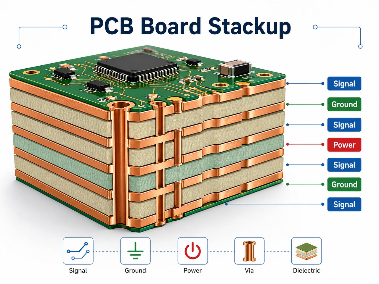
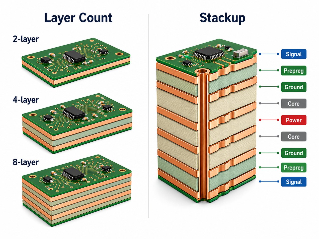
PCB board stackup cutaway showing signal, ground, power, dielectric, and via structures

What Is a PCB Board Stackup?

A PCB board stackup is the vertical construction of copper layers, cores, and prepregs within a circuit board. Each copper layer may be assigned to signals, ground, power, or a combination of these functions.

A complete stackup usually specifies:

  • Layer order and function
  • Core and prepreg materials
  • Dielectric thickness between copper layers
  • Inner and outer copper weight
  • Finished board thickness
  • Controlled impedance requirements

The terms PCB stack up, PCB board layer stackup, and PCB board stack generally describe the same structure.

A basic 4-layer board may use L1 for signals, L2 for ground, L3 for power, and L4 for signals. However, this layer sequence alone is not enough for fabrication. Electrical performance also depends on dielectric thickness, material Dk, copper thickness, and trace geometry.

What Is the Difference Between PCB Layer Count and PCB Stackup?

PCB layer count states how many conductive copper layers are present. PCB stackup defines how those layers are arranged and separated.

Item PCB Layer Count PCB Stackup
Main definition Number of copper layers Complete vertical board construction
Identifies layer function No Yes
Includes core and prepreg No Yes
Includes dielectric spacing No Yes
Supports impedance calculation No Yes
Used for lamination planning No Yes
Comparison between PCB layer count and full PCB stackup construction

Two PCBs may both have 4 copper layers but behave differently because their dielectric spacing, copper weight, and reference-plane arrangement are not the same.

For example, “4 layers, 1.6 mm thick” provides only basic quotation information. A more useful specification would include L2 as ground, L3 as power, 1 oz finished outer copper, 0.5 oz inner copper, FR-4 Tg170, and a defined 50-ohm impedance structure. The manufacturer can then select real core and prepreg combinations instead of estimating from layer count alone.

How Do You Decide How Many PCB Layers You Need?

The correct layer count is the lowest number that provides enough routing space, reference planes, power distribution, and manufacturing margin.

Layer Count Typical Applications Main Limitation
2 layers Basic controllers, relay boards, simple power supplies Limited routing space and less continuous ground coverage
4 layers MCU boards, IoT devices, industrial controls, communication modules May become restrictive with dense BGAs or many power rails
6 layers Mixed-signal systems, moderate BGA density, several high-speed interfaces Higher cost than 4 layers
8 layers FPGA, DDR, high-speed communication, complex power systems Requires more detailed stackup and impedance planning
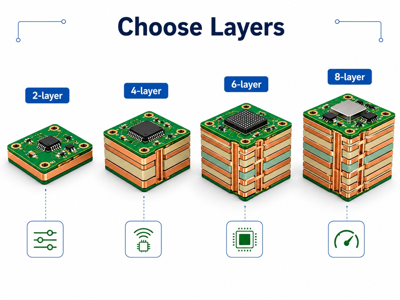
PCB layer selection comparison for 2-layer, 4-layer, 6-layer, and 8-layer boards

Routing density: More layers may be justified when traces require excessive detours, narrow spacing, or many vias. Increasing the PCB board size can create more routing area, but enclosure dimensions may not allow it.

Component packaging: Fine-pitch BGAs often determine the minimum practical layer count. Fan-out style, via diameter, pitch, and the number of signal rows all affect how many routing layers are required.

Signal speed: USB, Ethernet, HDMI, PCIe, and DDR interfaces benefit from continuous reference planes and controlled dielectric spacing. These interfaces can be difficult to manage on a 2-layer PCB even when the component count is modest.

Power distribution: A design with several voltage rails may require dedicated power regions or planes. A board with only 1 or 2 low-current rails may distribute power through traces and copper pours instead.

EMI and compliance: Adding ground planes can reduce loop area and improve return-path continuity, which becomes more valuable when the product must pass formal EMC testing.

Do not add layers only because a board contains a fast processor. Review the actual interfaces, package fan-out, routing channels, and reference requirements first.

How Should Signal, Ground, and Power Layers Be Arranged?

Critical signal layers should normally sit next to continuous reference planes. Ground is usually the preferred reference because it is less likely to be divided into isolated voltage regions.

Keep fast signals close to a reference plane. A short dielectric distance confines more of the electromagnetic field between the trace and its reference. This improves impedance control and reduces field spreading.

Avoid routing across plane splits. When a trace crosses a gap in its reference plane, return current must travel around the opening. The resulting loop can increase radiation, noise, and susceptibility.

Separate dense signal layers where possible. Two adjacent signal layers can couple through the dielectric, especially when long traces run in parallel. Placing a reference plane between them is usually preferable.

Keep power and ground close when the layer budget allows. A closely spaced power-ground pair provides plane capacitance and a compact current path. Local decoupling capacitors are still required at device power pins.

Maintain a balanced physical construction. Copper weight and dielectric thickness should be reasonably symmetrical around the center of the board. Large differences between the upper and lower halves can contribute to bow and twist.

What Is the Best 4-Layer PCB Stackup for Different Designs?

There is no single best 4-layer PCB stackup. The choice depends mainly on power complexity, routing space, and whether both outer signal layers require a solid ground reference.

4-Layer Structure Suitable For Main Trade-Off
Signal / Ground / Power / Signal General embedded and industrial boards Bottom-layer signals may reference a divided power plane
Signal + Power / Ground / Ground / Signal + Power Designs prioritizing EMI control and ground continuity Power routing consumes outer-layer space
Signal / Ground / Signal + Power / Ground Mostly top-side assembly or specialized routing Requires careful balance and reference-path review
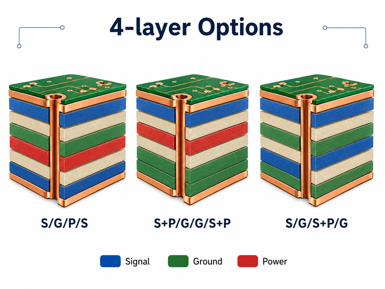
Three common 4-layer PCB stackup arrangements

Signal / Ground / Power / Signal: This conventional structure works well when the board has several power rails, most critical traces stay on L1, and bottom-layer signals do not cross gaps in the L3 power plane.

Signal + Power / Ground / Ground / Signal + Power: Both outer layers receive a nearby ground reference. It is practical when the design has few power rails and EMI performance matters more than having a dedicated power plane.

Signal / Ground / Signal + Power / Ground: This arrangement may suit a board with most components on the top side. It is a specialized option, so the L3 reference relationship, copper balance, placement, and lamination structure require careful review.

For many general-purpose products, Signal–Ground–Power–Signal remains a practical starting point. For designs with simple power distribution and tighter EMI targets, a dual-ground structure may provide better return-path control.

What Is a Practical 8-Layer PCB Stackup Example?

An 8-layer PCB stackup example should be selected according to signal-layer demand, power rails, and package fan-out. Copying a generic template without checking the routing plan can waste layers or create poor reference relationships.

Layer Function
L1 Components and high-speed signals
L2 Ground plane
L3 Signal
L4 Ground plane
L5 Power plane
L6 Signal
L7 Ground plane
L8 Components and signals
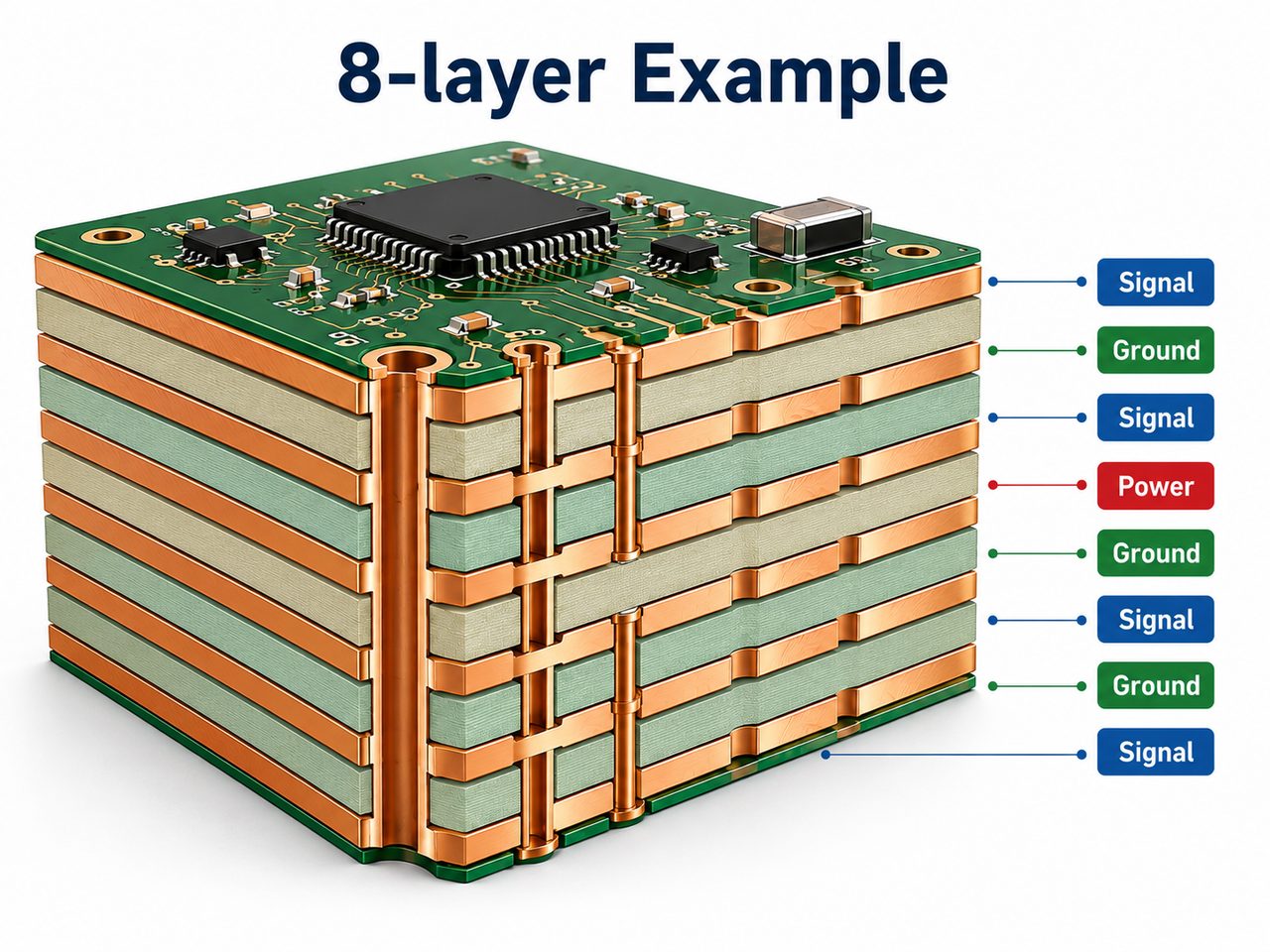
Practical 8-layer PCB stackup with signal, ground, and power layers

This structure provides several solid ground references and reduces reliance on a divided power layer. It can suit boards with fast clocks, DDR interfaces, sensitive analog sections, or demanding EMC targets.

An 8-layer structure becomes reasonable when 6 layers cannot support clean BGA breakout, multiple high-speed interfaces compete for routing space, or dedicated signal, ground, and power functions cannot fit comfortably.

The final arrangement still has to fit real core and prepreg options. A theoretically attractive stackup may be expensive or unstable if it depends on uncommon dielectric thicknesses.

How Do Core, Prepreg, Copper Weight, and Board Thickness Affect the Stackup?

Core, prepreg, and copper determine physical layer spacing and final board thickness. They also influence impedance, etching capability, current capacity, and mechanical stability.

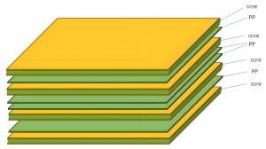
Core: A core is a fully cured laminate with copper bonded to one or both sides. Its thickness is relatively stable before multilayer pressing.

Prepreg: Prepreg is partially cured resin combined with glass fabric. During lamination, the resin flows and bonds adjacent layers. Pressed thickness depends on glass style, resin content, copper distribution, and pressing conditions.

Copper Weight Approximate Base Thickness Typical Use
0.5 oz 17 ”m Fine inner-layer routing
1 oz 35 ”m General signal and power circuits
2 oz 70 ”m Higher-current applications
3 oz and above 105 ”m and above Heavy-copper power boards

Outer-layer finished copper may be thicker than the starting foil because additional copper is deposited during through-hole plating. Thicker copper supports more current but also affects minimum trace width, spacing, and impedance geometry.

Common finished thicknesses include 0.8 mm, 1.0 mm, 1.2 mm, 1.6 mm, and 2.0 mm. The selected value may be driven by connector fit, enclosure dimensions, stiffness, impedance, assembly handling, or weight.

When possible, use core and prepreg materials the fabricator regularly stocks. Unusual combinations may increase cost, lead time, and batch-to-batch variation.

How Does PCB Stackup Affect Controlled Impedance and Signal Integrity?

Controlled impedance depends on the relationship between the trace and its surrounding stackup. Trace width is only one part of the calculation.

  • Finished trace width
  • Finished copper thickness
  • Dielectric thickness
  • Material dielectric constant
  • Reference-plane distance
  • Differential pair spacing
  • Solder mask
  • Microstrip or stripline geometry
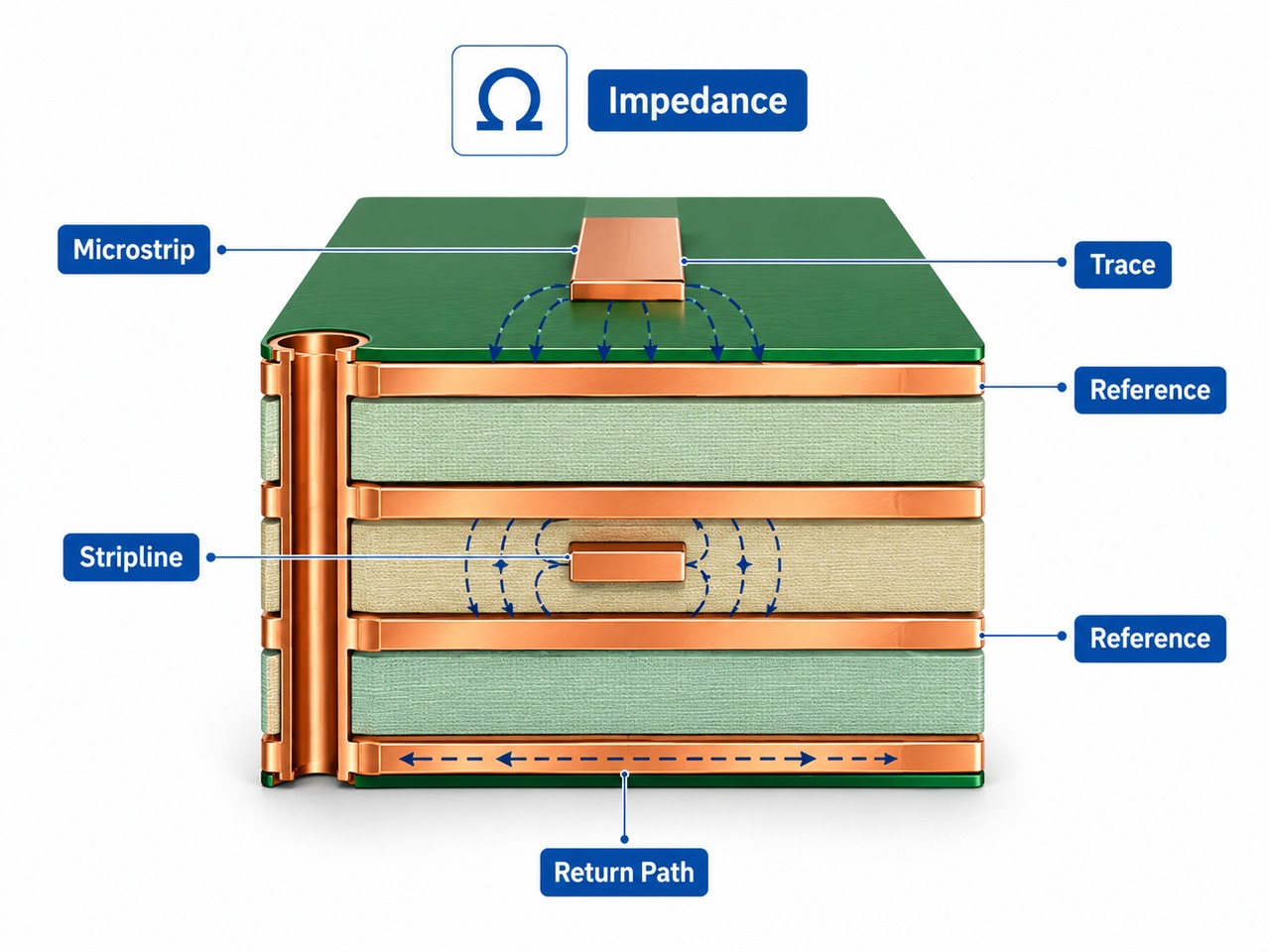
PCB controlled impedance diagram showing microstrip, stripline, reference planes, and return path

A surface microstrip is referenced to the plane beneath it. An internal stripline is placed between reference planes. These structures require different trace dimensions for the same target impedance.

Reducing the distance between a trace and its reference plane generally lowers impedance. The trace may then need to be narrowed to return to a 50-ohm target. Changes in copper thickness and material Dk also affect the result.

Reaching the calculated impedance value is not enough. The return path must remain continuous along the route. Common risks include crossing plane gaps, changing layers without nearby ground stitching vias, leaving long via stubs, and using Dk values that do not match the production laminate.

For controlled-impedance orders, the fabricator may adjust trace width or pair spacing to match actual dielectric and copper conditions. These changes should be approved before fabrication, especially around fine-pitch BGA fan-out areas.

What PCB Stackup Mistakes Cause EMI, Crosstalk, or Fabrication Problems?

Most stackup failures come from finalizing the layer arrangement before checking the real routing and production conditions.

  • Routing critical signals across split planes: This interrupts the return path and increases loop area.
  • Placing signal layers too far from their references: Wider field distribution makes EMI and impedance control more difficult.
  • Running long parallel traces on adjacent signal layers: Broadside coupling may increase crosstalk.
  • Using a divided power plane as though it were continuous: Signals may pass over several voltage regions.
  • Using nominal prepreg thickness in the impedance model: Pressed thickness may differ from the catalog value.
  • Creating an asymmetrical construction: Uneven copper and dielectric distribution can increase warpage.
  • Ignoring finished outer copper: Plating changes trace geometry and impedance.
  • Selecting uncommon material combinations: Procurement difficulty may raise cost and delay production.
  • Routing before confirming the stackup: Later impedance changes can force extensive layout revisions.
  • Copying an online structure without reviewing the circuit: A layer order that suits one design may restrict another.

A preliminary fabrication stackup is best requested before critical routing begins. At that stage, layer spacing, trace rules, and via structures can still be adjusted without redesigning the entire board.

What Should Be Confirmed with the PCB Manufacturer Before Finalizing the Stackup?

The manufacturer needs enough information to check lamination feasibility, impedance geometry, copper balance, and material availability.

  • Required layer count and layer functions
  • Finished board thickness and tolerance
  • Base material, Tg, Dk, or Df requirements
  • Inner and outer copper weight
  • Controlled impedance targets and tolerance
  • Target impedance layers and nets
  • Minimum trace width and spacing
  • Differential pair requirements
  • Through, blind, buried, or stacked vias
  • Sequential lamination requirements
  • Finished hole sizes and PCB board dimensions
  • Gerber, ODB++, or IPC-2581 files
  • NC drill files, fabrication drawing, and preliminary stackup drawing

A note such as “50-ohm impedance required” is incomplete unless the relevant layers, trace type, and tolerance are identified.

EBest Circuit, part of Best Technology, can review a proposed construction against available laminates, copper weights, via capabilities, and impedance targets. Review our PCB manufacturing capabilities when defining material, copper, via, impedance, and inspection requirements. This is particularly useful when the prototype must use the same basic material structure planned for volume production.

FAQs About PCB Board Stackup

Q1. What is a PCB board stackup?
A PCB board stackup is the ordered arrangement of copper and dielectric layers inside a circuit board. It defines signal, ground, and power layers together with core, prepreg, copper weight, and overall thickness.

Q2. Is PCB stackup the same as PCB layer count?
No. Layer count only states the number of copper layers. Stackup also defines their functions, spacing, materials, and electrical relationships.

Q3. What is the most common 4-layer PCB stackup?
Signal / Ground / Power / Signal is one of the most common structures. It is practical for many embedded and industrial products with several power rails.

Q4. Is Signal–Ground–Power–Signal always the best 4-layer stackup?
No. It works well for many boards, but bottom-layer signals may have poor return paths if the power plane is divided. A dual-ground structure may be better when ground continuity is the main priority.

Q5. How do I choose between a 4-layer and 6-layer PCB?
Move to 6 layers when 4 layers cannot provide enough routing channels, BGA breakout space, continuous references, or power distribution. Base the decision on the layout rather than component count alone.

Q6. What is a typical 8-layer PCB stackup?
A practical example is Signal / Ground / Signal / Ground / Power / Signal / Ground / Signal. The final sequence depends on power rails, signal density, and reference-plane requirements.

Q7. Should every signal layer be next to a ground plane?
Critical high-speed layers benefit from an adjacent ground plane. Low-speed layers may reference a continuous power plane, provided the return path is not interrupted.

Q8. Does PCB board size affect the required layer count?
Yes. A smaller board may require more layers because less routing area is available. Package density, interface speed, power structure, and connector placement are often more decisive.

Q9. How does PCB stackup affect controlled impedance?
It determines dielectric thickness, copper thickness, material Dk, and reference-plane distance used in the impedance calculation.

Q10. Can a PCB manufacturer change my proposed stackup?
The manufacturer may recommend different core or prepreg combinations to match available materials and production controls. Layer functions or electrical references should not be changed without design approval.

A practical PCB board stackup balances routing density, reference-plane continuity, power distribution, impedance, material availability, and production cost. Define the layer functions early, obtain a realistic fabrication structure, and complete critical routing using confirmed dielectric and copper parameters.

For a PCB board stackup review or PCB quotation, send your board files, layer requirements, copper weight, finished thickness, and impedance targets to sales@bestpcbs.com.
You may also like

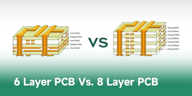
PCB 8 Layer Stackup: What Makes It Better Than 6-Layer?
Friday, November 21st, 2025

PCB 8 layer stackup​ is a specific arrangement of copper and insulating layers that provides an optimal balance of performance, density, and signal integrity for complex electronic designs. This article will provide a comprehensive guide to the standard 8 layer PCB stackup, compare it critically with 6-layer alternatives, and explore its key design considerations.

Are you struggling to decide if your high-speed or high-density design truly needs an 8-layer board, or if a 6-layer stackup would suffice?

  • ​Performance Anxiety:​​ Worrying that a 6-layer board might not provide sufficient isolation for sensitive signals, leading to crosstalk and electromagnetic interference (EMI).
  • ​Routing Congestion:​​ Facing the frustrating reality of not being able to route all the traces on a 6-layer board, especially with complex components like BGAs.
  • ​Impedance Mismatch:​​ Struggling to achieve consistent and controlled impedance for high-speed signals, which is more challenging with fewer layers.
  • ​Power Integrity Issues:​​ Experiencing noise on the power plane, which can cause erratic circuit behavior and is harder to manage in a 6-layer stackup.
  • ​Cost vs. Performance Dilemma:​​ Being caught between the lower cost of a 6-layer board and the superior performance and reliability of an 8-layer PCB, unsure of the right long-term investment.

The good news is that these challenges have clear solutions when you understand the advantages of a well-designed ​8 layer pcb stackup​ and partner with an experienced manufacturer.

  • ​Enhanced Signal Integrity:​​ An 8-layer stackup allows for dedicated signal layers adjacent to solid ground planes, effectively minimizing crosstalk and EMI, which directly addresses performance anxiety.
  • ​Superior Routing Capability:​​ The two additional layers provide much-needed real estate for routing complex designs, effortlessly solving routing congestion.
  • ​Precise Impedance Control:​​ With more layers, achieving a consistent dielectric environment for impedance-controlled traces (like for the ​8 layer PCB stackup impedance) becomes more straightforward and reliable.
  • ​Stable Power Delivery:​​ Dedicated power planes in an 8-layer stackup offer low-inductance power distribution, ensuring clean power to all components and eliminating power integrity issues.
  • ​Optimal Value Proposition:​​ While the initial cost is higher, the enhanced performance, reliability, and reduced need for re-spins often make the ​8 layer stackup pcb​ the more cost-effective solution for advanced applications, resolving the cost vs. performance dilemma.

At BEST Technology, we specialize in manufacturing high-quality, high-performance PCBs. As an original 8 layer PCB factory with 19 years of extensive experience in multilayer boards, we understand the intricacies of PCB 8 layer stackup design. We work with you to determine the optimal stackup, whether it’s a ​standard 8 layer PCB stackup​ or a more advanced ​8 layer HDI stackup, ensuring your design is built to the highest standards. A warm welcome to contact us at sales@bestpcbs.com to discuss your PCB 8 layer stackup project requirements.

PCB 8 Layer Stackup

​What is the Typical PCB 8 Layer Stackup?​​

A typical ​PCB 8 layer stackup​ is engineered to maximize performance by carefully alternating signal, plane, and dielectric layers. The arrangement is not random; it is designed to shield high-speed signals and provide stable power.

  • ​1. Standard Arrangement:​​ A common and effective ​typical 8-layer pcb stackup​ follows this sequence from top to bottom: Top Signal -> Ground Plane -> Inner Signal 1 -> Power Plane -> Ground Plane -> Inner Signal 2 -> Power Plane -> Bottom Signal. This “signal-plane-signal” pattern is a cornerstone of good ​8 layer pcb stackup design guidelines.
  • ​2. Shielding and Isolation:​​ This configuration provides shielding for the inner signal layers (Inner 1 and Inner 2) by placing them between ground planes. This is crucial for reducing noise and crosstalk.
  • ​3. Impedance Control:​​ The symmetric structure makes it easier to control the characteristic impedance of traces, which is vital for signal integrity.

In summary, the ​typical pcb 8 layer stackup​ is a balanced structure that prioritizes signal integrity, EMI control, and power stability, making it a versatile choice for many demanding applications.

​What are the Differences: 8 Layer PCB vs 6 Layer PCB?​​

The core difference in the “​8 layer PCB vs 6​” debate lies in the available resources for routing, shielding, and power distribution. The two extra layers in an 8-layer board provide a significant functional advantage.

  • ​1. Layer Configuration:​​ A standard 6-layer stackup might be: Signal – Ground – Signal – Signal – Power – Signal. This often forces high-speed signals to be routed on layers adjacent to other signal layers, increasing the risk of crosstalk. In contrast, the ​PCB 8 layer stackup​ provides dedicated internal routing layers between ground planes.
  • ​2. Performance:​​ The 8-layer board offers superior performance for high-speed designs due to better isolation and the ability to have dedicated power and ground planes. This leads to fewer signal integrity issues.
  • ​3. Cost and Complexity:​​ The ​6 layer PCB stackup​ is less expensive and simpler to manufacture. It is an excellent choice for many applications but can become a bottleneck for very high-speed or dense designs.

Ultimately, the choice hinges on the design’s complexity. For applications where signal integrity is paramount, the ​8 layer PCB motherboard​ or similar complex board is the clear winner.

PCB 8 Layer Stackup

How Thick is an 8 Layer PCB?​​

The ​standard thickness of a PCB stackup​ is often, but not always, around 1.6mm (0.063 inches). However, the final ​8 layer PCB thickness​ is a result of the materials used and the number of layers.

  • ​1. Standard and Custom Thickness:​​ While 1.6mm is common, the thickness can vary. The ​standard 8 layer PCB stackup​ thickness can be designed to be 0.8mm, 1.0mm, 1.6mm, or even thicker based on the application’s mechanical and electrical requirements.
  • ​2. Factors Influencing Thickness:​​ The ​8 layer PCB stackup thickness​ is determined by the thickness of the core and prepreg (insulating) materials, as well as the copper weight. For impedance control, the dielectric thickness between a signal layer and its reference plane is critical.
  • ​3. Importance of Specification:​​ When discussing your ​PCB 8 layer stackup​ with a manufacturer, it is essential to specify your desired finished thickness and impedance requirements to ensure the stackup is designed correctly.

Therefore, the thickness of an 8-layer PCB is not a fixed value but a key parameter that is carefully engineered during the stackup design phase.

​How to Calculate the 8 Layer PCB Stackup Impedance?​​

Calculating the ​8 layer PCB stackup impedance​ is a critical step for high-speed design, ensuring signals are transmitted without reflection or distortion.

​1. Key Parameters:​​ The characteristic impedance of a trace depends on its width (W), the dielectric height (H) to the reference plane, and the dielectric constant (Er) of the insulating material. The copper thickness (T) also has a minor effect.

2. ​Use of Formulas and Tools:​​ While formulas exist, e.g., for microstrip:

PCB 8 Layer Stackup

Most engineers use impedance calculation tools provided by manufacturers or integrated into PCB design software like ​8 layer PCB stackup altium. These tools automatically calculate the required trace width for a target impedance (e.g., 50Ω or 100Ω differential) based on the defined stackup.

​3. Manufacturer Collaboration:​​ It is best practice to finalize your stackup with your PCB manufacturer. They can provide the most accurate Er values and ensure the fabricated board will meet your impedance targets.

Proper impedance calculation is non-negotiable for reliable high-speed performance and is a fundamental part of the ​8 layer PCB stackup design guidelines.

​How Many Layers can a PCB Have?​

PCBs can have a vast number of layers, from 1 to over 50 in extreme cases like advanced servers. The more pertinent question is: do PCB layers matter? The answer is an emphatic yes.

  • ​1. Function of Layers:​​ The number of ​PCB board layers​ directly determines the board’s functionality. More layers allow for more complex circuitry, better separation of analog and digital sections, improved power integrity, and superior signal integrity through proper referencing and shielding.
  • ​2. Choosing the Right Number:​​ A simple electronic device might only need a ​PCB stackup 4 layer, while a smartphone motherboard might require 10 or 12 layers. The decision for a ​PCB 8 layer stackup​ is based on the need for a robust design that can handle multiple high-speed signals and multiple power supplies efficiently.

The number of layers is a fundamental architectural decision that impacts the cost, performance, and reliability of the final product.

​What is the 4 Layer PCB Rule?​​

​The “4 layer PCB rule” is a fundamental guideline in PCB design that dictates the optimal arrangement of layers to maximize performance while minimizing cost. It serves as a crucial stepping stone towards understanding more complex stackups like the 8-layer board. While not a rigid law, following this rule is considered a best practice for most 4-layer designs.

  • ​1. The Core Principle: Dedicated Plane Layers​
    The most important aspect of the rule is the allocation of the two internal layers.
    Instead of using them for additional signal routing, they are dedicated exclusively as solid, uninterrupted planes—one for ground (GND) and one for power (PWR).
    The outer layers (Top and Bottom) are then used for component placement and signal routing.
  • ​2. Standard Layer Stackup​
    A typical and effective ​4 layer board stackup​ follows this sequence:
    • ​Layer 1 (Top):​​ Components and Signal Routing
    • ​Layer 2 (Internal):​​ Ground Plane (GND)
    • ​Layer 3 (Internal):​​ Power Plane (PWR)
    • ​Layer 4 (Bottom):​​ Components and Signal Routing
  • ​3. Key Benefits of This Rule​
    • ​Improved Signal Integrity:​​ By routing signals on the outer layers adjacent to the solid internal planes, each signal trace has a clear and continuous reference plane.
      This controlled environment is essential for managing characteristic impedance and significantly reducing electromagnetic interference (EMI) and crosstalk.
    • ​Enhanced Power Integrity:​​ The dedicated power plane provides a low-inductance path for distributing power to all components, resulting in a cleaner and more stable voltage supply, which reduces noise.
    • ​Superior EMI Performance:​​ The two internal planes act as shields, containing the electromagnetic fields generated by high-speed signals on the outer layers, making the board less susceptible to emitting and receiving interference.
  • ​4. Comparison to 2-Layer Boards​
    This rule highlights the major leap in performance from a 2-layer to a ​PCB stackup 4 layer.
    A 2-layer board lacks dedicated planes, forcing signals and power to share routing space, which often leads to noise and reliability issues.

In summary, the ​4 layer PCB rule​ is a foundational concept that prioritizes a clean and stable electrical environment. It establishes the core principles of using dedicated power and ground planes, which are then scaled up and refined in more advanced stackups like the ​8 layer PCB stackup.

​8 Layer PCB Stackup Design Guidelines

​Adhering to proven ​8 layer PCB stackup design guidelines​ is fundamental to achieving optimal signal integrity, power integrity, and EMC performance. While the previous section outlined four key principles, a deeper understanding requires grounding these rules in the fundamental goals of all stackup design.

Before delving into specifics, all stackup design aims to satisfy two primary rules:

  1. ​A Reference Plane for Every Signal Layer:​​ Every high-speed signal routing layer must be adjacent to a solid reference plane (power or ground). This provides a controlled impedance path and a clear, low-inductance return path for signals.
  2. ​Tight Power-Ground Coupling:​​ Closely spaced power and ground planes are crucial. The minimal spacing between them creates a natural, high-frequency decoupling capacitor that enhances power integrity and reduces EMI.

​Understanding the limitations of simpler boards highlights the necessity of a well-designed 8-layer stackup.

  • ​Single/Double-Sided Boards:​​ These lack dedicated planes, leading to large signal loop areas which are major sources of EMI and susceptibility. The primary mitigation is to route critical signals (like clocks) with an adjacent ground trace to minimize the loop area.
  • ​Four-Layer Boards:​​ While a significant improvement, the standard 1.6mm board thickness creates a large separation between layers, weakening power-ground coupling and making impedance control challenging. The best 4-layer stackup for EMI (GND-SIG/PWR-SIG/PWR-GND) uses outer layers as ground planes for shielding.
  • ​Six-Layer Boards:​​ These offer a better balance. A common good stackup is SIG-GND-SIG-PWR-GND-SIG. It provides a reference plane for each signal layer and pairs the power and ground layers. However, achieving tight power-ground coupling within a standard board thickness remains difficult.

​An 8-layer board provides the canvas to implement near-ideal stackup design. Here are critical guidelines, moving beyond the basics.

  1. ​Prioritize Shielding and Symmetry to Prevent Warping​
    The simplest 8-layer stackup (e.g., SIG-SIG-GND-SIG-SIG-PWR-SIG-SIG) is inherently poor. It has multiple consecutive signal layers without reference planes, leading to poor SI and EMI. A superior approach uses symmetry and multiple ground planes. A ​highly recommended 8 layer stackup​ is:
    • Top Signal (Microstrip)
    • Ground Plane
    • Internal Signal 1 (Stripline)
    • Power Plane
    • Ground Plane
    • Internal Signal 2 (Stripline)
    • Power Plane
    • Bottom Signal (Microstrip)
      This arrangement is symmetrical, preventing warping. The internal signal layers are shielded between planes, and the ground planes act as excellent EMI shields.
  2. ​Maximize Interplane Capacitance for Power Integrity​
    Following the core rule of tight coupling, place the power and ground planes that require the best noise immunity (e.g., the core voltage for an FPGA) as adjacent layers (e.g., L4/L5 or L6/L7 in the stackup above). The thin dielectric between them creates a large, low-inductance distributed capacitor that effectively suppresses high-frequency noise on the power rail.
  3. ​Select the Optimal Stackup for Your EMC and SI Goals​
    The provided material describes three common 8-layer configurations. The best choice depends on your priority:
    • ​Good SI, Poor EMI (Example 1):​​ Features many signal layers but lacks sufficient shielding, making it susceptible to radiating.
    • ​Good SI, Better EMI (Example 2):​​ This is a strong, common choice. It uses outer ground planes for shielding and has a tightly coupled power-ground plane pair in the center. It offers an excellent balance for most applications.
    • ​Best SI and EMI (Example 3):​​ This is the premium configuration, utilizing four ground planes. It provides the highest level of shielding and the cleanest possible return paths for all signals, making it ideal for extremely noise-sensitive or high-radiation applications.
  4. ​Collaborate with Your Manufacturer Early for Impedance Control​
    This guideline cannot be overstated. Once you have a target stackup, you must work with your PCB manufacturer before finalizing the design. Provide them with your target impedances (e.g., 50Ω single-ended, 100Ω differential). They will feedback the precise dielectric thicknesses and trace widths required to hit your targets based on their specific materials and process capabilities. This is a non-negotiable step in the ​8 layer pcb stackup design guidelines.

In summary, designing an 8-layer stackup is an exercise in careful layer ordering to manage return paths, provide shielding, and ensure stable power. By moving from the basic rules to these advanced guidelines—prioritizing shielded stripline layers, tight power-ground coupling, and selecting a stackup based on EMC needs—you can fully leverage the capabilities of an 8-layer board to create a robust, high-performance product.

​How is the 8 Layer HDI Stackup?​​

​An ​8 layer HDI stackup​ represents a significant advancement over a standard ​8 layer PCB stackup​ by incorporating High-Density Interconnect (HDI) technologies. It is designed for the most space-constrained and performance-driven applications where miniaturization and complex routing are paramount.

  • ​1. Core HDI Technologies​
    HDI stackups are defined by their use of advanced manufacturing processes:
    • ​Microvias:​​ These are laser-drilled vias with a much smaller diameter (typically less than 150”m) than mechanically drilled through-hole vias. They allow for connections between adjacent layers (e.g., from Layer 1 to Layer 2) with a minimal footprint.
    • ​Finer Traces and Spaces:​​ HDI processes enable the etching of much narrower trace widths and clearances, allowing more circuitry to be packed into a smaller area.
    • ​Advanced Build-Up Structures:​​ HDI boards are often built using a sequential lamination process, creating complex sub-composites that can include stacked microvias, staggered vias, and buried vias.
  • ​2. Design Advantages over Standard 8-Layer Stackups​
    The integration of HDI technology into an ​8 layer stackup PCB​ offers several critical benefits:
    • ​Extreme Miniaturization:​​ By using microvias and finer lines, components can be placed closer together, and the overall board size can be drastically reduced. This is essential for devices like modern smartphones, wearables, and IoT sensors.
    • ​Enhanced Signal Performance:​​ Shorter pathways and reduced via stubs from microvias lead to better electrical performance at high frequencies, minimizing signal loss and reflection.
    • ​Greater Routing Density:​​ HDI allows for escape routing from high-pin-count components like fine-pitch BGAs, which would be impossible to route on a standard ​8 layer PCB motherboard​ of the same size.
    • ​Improved Reliability:​​ The materials and processes used in HDI manufacturing often result in a more robust and reliable board.
  • ​3. Typical Applications​
    An ​8 layer HDI stackup​ is not for every project due to its higher cost. It is typically reserved for cutting-edge applications, including:
    • Smartphones and Tablets
    • Advanced Medical Implants and Diagnostic Equipment
    • High-Performance Computing and Networking Hardware
    • Aerospace and Defense Avionics

In conclusion, the ​8 layer HDI stackup​ is the pinnacle of dense, high-performance PCB design. While a standard ​typical 8-layer PCB stackup​ is powerful, the HDI variant pushes the boundaries of what’s possible, enabling the creation of smaller, faster, and more complex electronic devices.

​What are the Applications of 8 Layer Stackup PCB?​​

An 8-layer PCB stackup is widely used in advanced electronic systems where designers need strong signal integrity, stable power delivery, and compact circuit density. These boards support high-speed interfaces, complex processors, and mixed-signal architectures that cannot be achieved with simpler stackups.

Typical applications include:

  • 8-layer PCB motherboards for industrial and embedded computing
  • High-speed network devices such as routers, switches, and 5G baseband units
  • Telecommunications infrastructure with dense RF and digital circuits
  • Automotive electronics including ADAS domain controllers
  • Medical imaging and diagnostic systems
  • Industrial automation and rugged control equipment

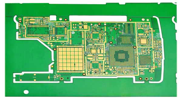
To show how a real design translates into actual applications, the following example highlights a high-performance 8-layer HDI PCB with engineering features tailored to demanding markets. And the following specific applications are supported by a PCB built to these professional specifications:

  • Via Type: Resin-filled buried and blind vias
  • Layer Count: 8-Layer
  • Material: High-Tg FR-4
  • Tg Rating: 180°C
  • Copper Weight: 1oz outer / 1oz inner
  • Surface Finish: ENIG (1ÎŒâ€ł)
  • Solder Mask: Green
  • Silkscreen: White
  • Final Thickness: 1.6mm
  • Technology: 3-step HDI

1. Core Networking & Communication Systems

Application: Processing and switching board for 100G/200G/400G network equipment.

Why an 8-layer PCB fits:
The 3-step HDI structure handles fine-pitch BGA components used in high-bandwidth ASICs and FPGAs. Meanwhile, TG180 FR-4 improves thermal stability during long-term, high-load operation. This combination supports multi-lane SerDes signals and tight impedance control for high-speed communication links.

2. Aerospace and Defense Electronics

Application: Signal processing module for airborne radar or mission-critical avionics.

Why an 8-layer PCB fits:
Aircraft electronics experience extreme temperature swings and continuous vibration. 1.6mm finished thickness and TG180 laminate provide strong mechanical strength and thermal endurance. The 1ÎŒâ€ł ENIG finish offers reliable surface quality for gold-wire bonding and high-frequency interconnects common in RF signal chains.

3. Advanced Medical Imaging Equipment

Application: Core electronic module in portable ultrasound or digital imaging diagnostics.

Why an 8-layer PCB fits:
Medical devices demand both miniaturization and signal clarity. HDI + resin-filled vias help integrate dense components into a compact format while maintaining stable impedance for sensitive analog/digital imaging circuits. The ENIG surface ensures excellent contact reliability for fine-pitch connectors and probe interfaces.

4. Next-Generation Automotive Electronics

Application: Central computing board for ADAS or autonomous driving systems.

Why an 8-layer PCB fits:
ADAS controllers must process multiple high-resolution camera, radar, and LiDAR inputs. An 8-layer stackup provides robust isolation between high-speed differential pairs and noisy power circuits. The 1oz copper thickness supports steady power delivery to high-current SoCs and processing units, ensuring stable performance even at elevated vehicle temperatures.

5. Industrial IoT and Edge Computing Devices

Application: Industrial edge gateway, PLC controller, or machine-vision interface.

Why an 8-layer PCB fits:
Factories require devices that remain stable under dust, humidity, vibration, and electrical noise. The ENIG finish prevents oxidation, and the green solder mask + white silkscreen combination improves maintenance visibility. The rigid 8-layer architecture enhances long-term reliability for 24/7 operation in challenging industrial environments.

In closing, this example makes it clear that an 8-layer PCB stackup is far more than a simple increase in layer count. With the right combination of materials, HDI structures, and controlled-impedance routing, it becomes a powerful platform for mission-critical, high-speed, and high-density electronic systems across multiple industries.

PCB 8 Layer Stackup

In conclusion​, PCB 8 layer stackup​ is a sophisticated multilayer board configuration that offers a significant performance upgrade over 6-layer alternatives for demanding electronic applications. This article has explored the structure, advantages, and design considerations that make the 8-layer stackup a preferred choice for high-speed and high-density designs.

For engineers seeking reliable, high-performance PCB 8 layer stackup​ fabrication, partnering with an experienced 8 layer PCB manufacturer is crucial. At BEST Technology, we have the expertise to guide you through the entire process, from selecting the ​best 8 layer stackup​ for your needs to ensuring impeccable manufacturing quality. Pls feel free to contact us at sales@bestpcbs.com to get started on your next 8 layer stackup PCB project.

You may also like

8-Layer PCB Stackup Design Guide | EBest Circuit (Best Technology)
Friday, July 11th, 2025

Designing a reliable multilayer circuit board starts with getting the stackup right. If your project involves high-speed signals, compact layouts, or reduced EMI, an 8-layer PCB stackup is a solid choice. It offers flexibility, better performance, and room for complex routing.

In this guide, we’ll walk you through everything you need to know—layer configurations, materials, sizes, and how to make the most of this structure with the help of a trusted PCB manufacturer.

8-Layer PCB Stackup Design Guide

What is a PCB Stackup?

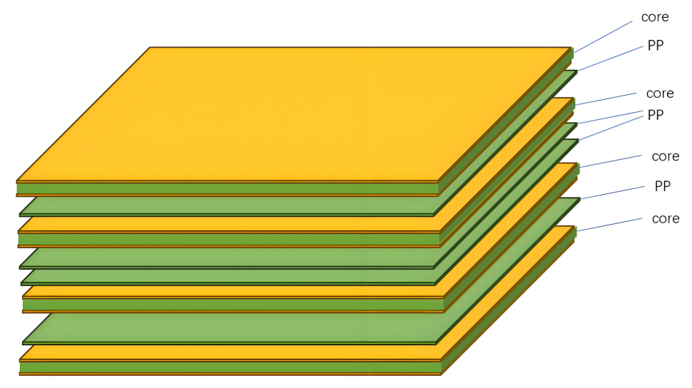
A PCB stackup is the arrangement of copper layers and insulating materials inside a circuit board. These layers are stacked and bonded together using prepreg (resin-impregnated fiberglass) and core materials. The goal is to create a reliable board that supports both mechanical strength and excellent electrical performance.

In simple words, the stackup decides how signal layers, power planes, and ground layers are placed in the board. In high-speed digital designs, this structure plays a big role in signal quality, electromagnetic compatibility (EMC), and overall performance.

For an 8-layer PCB, the stackup consists of eight layers of copper with alternating dielectric materials. These are usually divided into four signal layers and four plane layers, though that can change based on your design needs.

PCB Stackup Considerations

For most PCB designs, there are often competing requirements between electrical performance, manufacturing limitations, cost targets, and system complexity. The final PCB stackup is usually a result of careful trade-offs across these factors. High-speed digital circuits and RF systems commonly rely on multilayer boards for better control and performance. Below are 8 essential principles to consider when designing a reliable stackup:

1. Layer Arrangement

In multilayer PCBs, you’ll typically work with signal layers (S), power planes (P), and ground planes (GND). Power and ground planes are usually solid, unbroken areas that provide low-impedance return paths for signal currents. Signal layers are often positioned between these planes to form symmetrical or asymmetrical stripline structures. The top and bottom layers are mainly used for component placement and limited routing. It’s best to keep traces on these outer layers short to reduce direct radiation and EMI.

PCB Stackup Considerations

2. Defining a Single Power Reference Plane

Decoupling capacitors are vital for maintaining power integrity, and they can only be placed on the outer layers of the PCB. The trace length, pad design, and vias connected to these capacitors greatly affect their effectiveness. To improve decoupling, make these connections short and wide, and minimize via length. For example, in a high-speed digital system, place decoupling capacitors on the top layer, dedicate the second layer to power for the processor, use the third layer for signal routing, and assign the fourth layer as a ground reference.

3. Incorporating Multiple Ground Planes

Using multiple ground planes helps create low-impedance return paths and minimizes common-mode EMI. Ground and power planes should be tightly coupled, and signal layers should also be close to reference planes. Reducing the dielectric thickness between layers improves coupling and enhances performance.

4. Managing Multiple Power Planes

When your design includes more than one power plane, these planes are often split into different voltage regions. If a signal layer is placed next to a multi-region power layer, signal currents may not find clean return paths, leading to noise or EMC issues. For high-speed digital signals, avoid routing traces near split power planes to prevent return current discontinuities.

5. Designing Signal Routing Pairs

When a signal travels from one layer to another, it creates what’s known as a “routing pair.” Ideally, the return current should stay within the same reference plane when switching layers. In practice, however, signals often need to transition between layers. To maintain signal integrity, ensure that return paths are available through stitching vias or decoupling capacitors. Using adjacent layers as routing pairs is a practical and effective strategy.

6. Routing Direction Guidelines

Keep trace directions consistent within each signal layer. At the same time, rotate the routing direction between adjacent signal layers. For instance, use horizontal routing (X-axis) on one layer and vertical routing (Y-axis) on the next. This practice reduces crosstalk and improves signal clarity.

7. Even-Layer Designs is Better

Although odd-layer PCBs may appear cheaper due to fewer materials, they’re more expensive to manufacture. That’s because odd-layer boards require non-standard lamination processes and additional handling steps. These increase the risk of surface damage, incorrect etching, and longer production times. In contrast, even-layer PCBs are more stable, cost-effective, and easier to produce at scale.

PCB Stackup Considerations

8. Budget

Multilayer PCBs are naturally more expensive than single- or double-layer boards. However, they offer significant benefits in functionality, miniaturization, EMI control, and signal integrity. When weighing total cost versus performance, the difference between multilayer and simpler boards may not be as high as expected.

Standard 8-Layer PCB Stackup Structure

When it comes to multilayer PCB design, the arrangement of signal, power, and ground layers directly affects signal integrity, EMI performance, and power delivery. Below are three common 8-layer stackup configurations, each with its own strengths and limitations.

Standard 8-Layer PCB Stackup Structure

Option 1:

Layer 1: Signal 1

Layer 2: Signal 2

Layer 3: Ground

Layer 4: Signal 3

Layer 5: Signal 4

Layer 6: Power

Layer 7: Signal 5

Layer 8: Signal 6

This layout alternates signal and power layers but does not take full advantage of the electromagnetic shielding benefits that a multilayer board can offer. The ground and power planes are separated, reducing the board’s EMI suppression capability. In addition, the power distribution network suffers from higher impedance, which may affect voltage stability in high-speed or high-current applications.

Option 2:

Layer 1: Signal 1

Layer 2: Ground

Layer 3: Signal 2

Layer 4: Power

Layer 5: Ground

Layer 6: Signal 3

Layer 7: Ground

Layer 8: Signal 4

This structure is widely regarded as the optimal 8-layer PCB stackup. It provides excellent electromagnetic shielding through the use of multiple ground planes. Each signal layer is placed adjacent to a reference plane (either ground or power), which improves signal stability and impedance control. Additionally, the tight coupling between power and ground planes enhances EMI performance and power integrity. This setup is ideal for high-speed, high-frequency, or noise-sensitive applications.

Option 3:

Layer 1: Signal 1

Layer 2: Ground

Layer 3: Signal 2

Layer 4: Power

Layer 5: Ground

Layer 6: Signal 3

Layer 7: Power

Layer 8: Signal 4

This configuration is a variation of Option 1 with improved EMI performance. By adding an extra reference plane, it provides better control over the characteristic impedance of the signal layers. However, the placement of the second power plane (with limited coupling to a nearby ground) leads to higher power delivery impedance, which could be a drawback in power-sensitive designs. Some optimization in power layer arrangement is still needed.

8-Layer PCB Stackup Materials

The performance of an 8-layer PCB stackup relies heavily on the materials used between and around its copper layers. These materials affect everything from electrical behavior to thermal stability and even mechanical strength. Let’s look at the two main categories: conductive and dielectric materials.

1. Conductive Layers

Copper is the most common metal used for the conductive layers in an 8-layer PCB. It’s highly conductive, easy to work with, and available in different thicknesses and finishes.

  • Copper Thickness: Most boards use œ oz or 1 oz copper per layer. If the design needs to handle higher current, 2 oz or thicker copper may be used.
  • Copper Type: Standard copper foil is either electrodeposited (ED) or rolled. Rolled and annealed copper is smoother and more flexible, which makes it useful in boards that need better bend resistance.
  • Surface Finishes: The exposed copper is usually treated with a surface finish to protect it and ensure solderability. Options include HASL, ENIG, OSP, and immersion silver, among others.

2. Dielectric Layers

The dielectric materials are the insulating layers that separate the copper traces. These layers are critical for controlling impedance, heat flow, and electrical isolation.

  • FR-4: A glass-reinforced epoxy laminate, FR-4 is the most common dielectric for general-purpose PCBs. It’s reliable, widely available, and cost-effective.
  • High-Frequency Materials: For RF and high-speed digital designs, materials with low dielectric loss—like PTFE (Teflon), ceramic-filled PTFE, or hydrocarbon-based ceramics—are preferred. These support better signal integrity at high frequencies.
  • Thermal Conductive Materials: When heat dissipation is a concern, substrates like alumina or aluminum nitride are used. These materials offer higher thermal conductivity than standard epoxy systems.

To hold everything together, manufacturers use prepregs—uncured fiberglass sheets soaked in resin. Common prepreg materials include FR-4 for standard designs and polyimide for higher thermal or mechanical stress environments.

At the center of the stackup is the core, which acts like a spine for the board. This rigid layer typically uses FR-4 or polyimide, though in some high-power or high-heat applications, metal cores are added to improve thermal performance.

8-Layer PCB Thickness & Sizes

The total thickness of an 8-layer PCB depends on several factors:

  • Copper thickness: Common values are 0.5oz, 1oz, or 2oz per layer.
  • Prepreg/Core thickness: Adjusted to achieve specific impedance and board height.
  • Number of plane vs signal layers: Affects thermal and mechanical behavior.

Common Thickness Options:

  • 1.6mm (0.063″) – Industry standard, suitable for most applications.
  • 2.0mm to 2.4mm – Used when extra copper is needed for higher current.
  • 3.2mm or custom – Selected for industrial or military-grade boards.

PCB Sizes:

Panel sizes are typically 18” x 24” before routing. Your board can be as small as a few millimeters or as large as the full panel, depending on the application.

6 Layer vs 8 Layer PCB

A 6-layer PCB consists of six layers of copper circuitry stacked with insulating layers (prepreg and core) in between. It usually includes:

  • 4 Signal Layers for routing high- and low-speed signals
  • 1 Power Plane to distribute voltage
  • 1 Ground Plane to provide a return path and help with EMI suppression

A typical 6-layer stackup looks like this:

Layer 1: Signal (Top)

Layer 2: Ground

Layer 3: Signal

Layer 4: Signal

Layer 5: Power

Layer 6: Signal (Bottom)

While both 6-layer and 8-layer PCBs are widely used in advanced electronics, they serve slightly different purposes depending on design complexity, signal speed, and EMI requirements. Let’s compare them together:

Aspect6-Layer PCB8-Layer PCB
Layer Count68
Typical Configuration4 signal layers + 1 power + 1 ground4 signal layers + 2 power + 2 ground
Routing SpaceModerateMore routing room
Signal IntegrityGood, suitable for most mid-speed signalsExcellent, supports very high-speed signal routing
EMI ShieldingLimited shielding with fewer ground planesStrong EMI control due to multiple ground planes
Power DistributionSingle power plane, higher impedanceDual power planes, better PDN performance
Design ComplexityLess complex, easier to design and fabricateMore complex, better for advanced designs
Thermal PerformanceAdequate for medium power applicationsBetter heat spreading for high-power components
CostLower fabrication costHigher cost due to more layers and materials
Use CaseMid-level MCUs, general embedded, basic RFFPGAs, DDR memory, high-speed data buses, complex SoCs

Use a 6-Layer PCB if:

  • Your design isn’t extremely dense.
  • The signals don’t require tight EMI control.
  • You want to balance performance and cost.
  • There’s no strict need for multiple ground or power planes.

It’s widely used in commercial electronics that don’t involve ultra-high-speed communication or compact multilayer routing challenges.

Choose an 8-Layer PCB when:

  • High-speed signals (such as PCIe, USB 3.x, DDR4, or SERDES) are involved.
  • EMI performance is critical, especially in sensitive industrial or medical devices.
  • You need more space for routing due to a denser component layout.
  • Stable power delivery is required across multiple voltage domains.
  • You’re working with a compact form factor that demands vertical signal distribution.

An 8-layer stackup allows designers to pair every signal layer with a nearby ground or power plane, which significantly improves signal quality and reduces noise.

Benefits of Working with an Experienced PCB Manufacturer

Designing and fabricating an 8-layer PCB stackup requires precise engineering and process control. Partnering with a reliable manufacturer like EBest Circuit (Best Technology) brings several benefits:

1. Stackup Design Assistance: Professional help with impedance control, signal integrity, and EMC optimization.

2. Material Expertise: Guidance in choosing suitable laminates for your specific requirements.

3. Advanced Fabrication: Capability to handle HDI, blind/buried vias, and tight tolerances.

4. Quality Assurance: Rigorous testing like AOI, X-ray, and impedance measurement.

5. Fast Turnaround: Efficient production process without sacrificing quality.

Why Choose EBest Circuit (Best Technology) for Your 8-Layer PCB Stackup?

EBest Circuit (Best Technology) is a trusted 8-layer PCB stackup specialist serving global customers across aerospace, medical, automotive, and industrial electronics. We hold certifications including:

  • ISO9001 for quality control
  • ISO13485 for medical electronics
  • IATF16949 for automotive-grade PCBs
  • AS9100D for aerospace applications

Our engineers assist with DFM check, impedance control, EMI reduction, thermal management, and material choices, ensuring your 8-layer design performs reliably under real-world conditions.

FAQs

1. What is the best layer configuration for an 8-layer PCB stackup?

A balanced configuration like Signal–GND–Signal–Power–GND–Signal–Power–Signal is often preferred for signal integrity and EMI control.

2. How much does an 8-layer PCB cost?

Cost varies by material, size, copper weight, and complexity, but typically ranges from $50 to $300 per board in small batches.

3. What software is used for 8-layer PCB design?

Tools like Altium Designer, Eagle, KiCAD, and OrCAD support multilayer PCB stackup planning and layout.

4. Can you use HDI features in 8-layer PCBs?

Yes. Blind and buried vias, via-in-pad, and microvias are often used in 8-layer HDI designs.

5. How do I choose the right manufacturer for 8-layer PCBs?

Look for certifications, material options, engineering support, and experience with multilayer stackups—like what EBest Circuit (Best Technology) provides.

You may also like