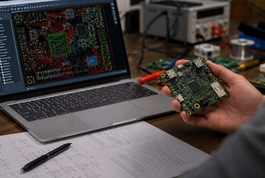
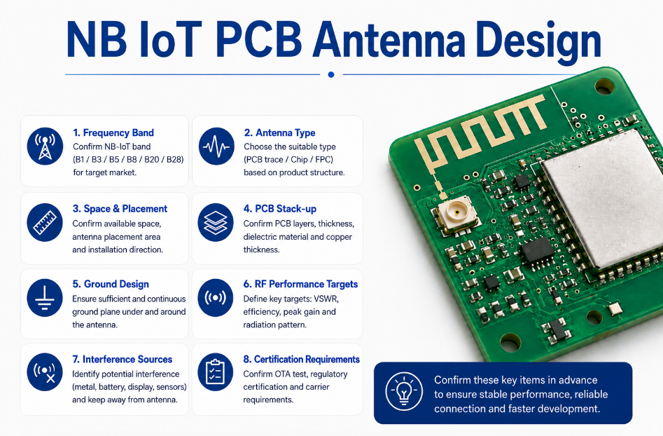
Is your robotics PCB still stable after motor startup, sensor feedback and real motion testing? Many robotics PCB problems do not appear during basic power-on checks. They usually appear when the motor starts, the sensor begins sending feedback, or the robot runs under vibration and heat. At that stage, voltage drop, signal noise, AI module heating and weak connector soldering can delay the whole project.
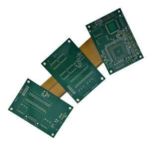
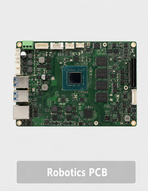
EBest is a China source factory for robotics PCB manufacturing, PCB assembly, component sourcing and testing. Founded in 2006, EBest supports motion control PCB, sensor PCB, robot power PCB and AI module PCB from prototype to mass production, helping robot projects move from early validation to stable batch production.
What Robotics PCB Problems Can EBest Help You Prevent?
EBest helps prevent unstable power, motor interference, sensor errors, AI module heating, solder joint failure and inconsistent batch quality before delivery. These issues often appear after basic power-on testing, especially when the robot starts moving under real motor load and vibration.
Common robotics PCB risks include:
- Motor startup voltage drop that causes random reset
- Sensor noise that affects detection and feedback
- AI module heating that reduces long-term reliability
- Weak connector soldering that fails under movement
- Poor assembly consistency between prototype and batch production
- Component sourcing delay before mass production
- Insufficient testing before final delivery
A robotics PCB manufacturer should not only fabricate the board. It should review production risks, control soldering quality, check component availability and support testing before delivery.
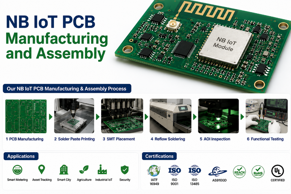
How Does EBest Support Robotics PCB Manufacturing?
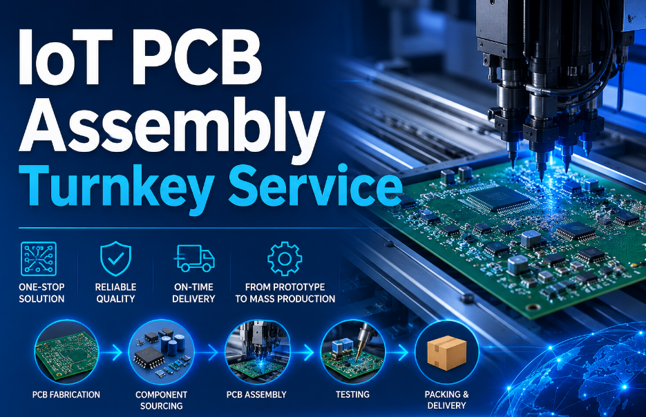
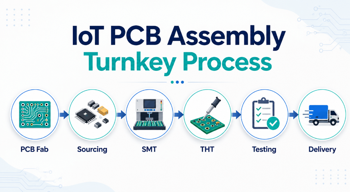
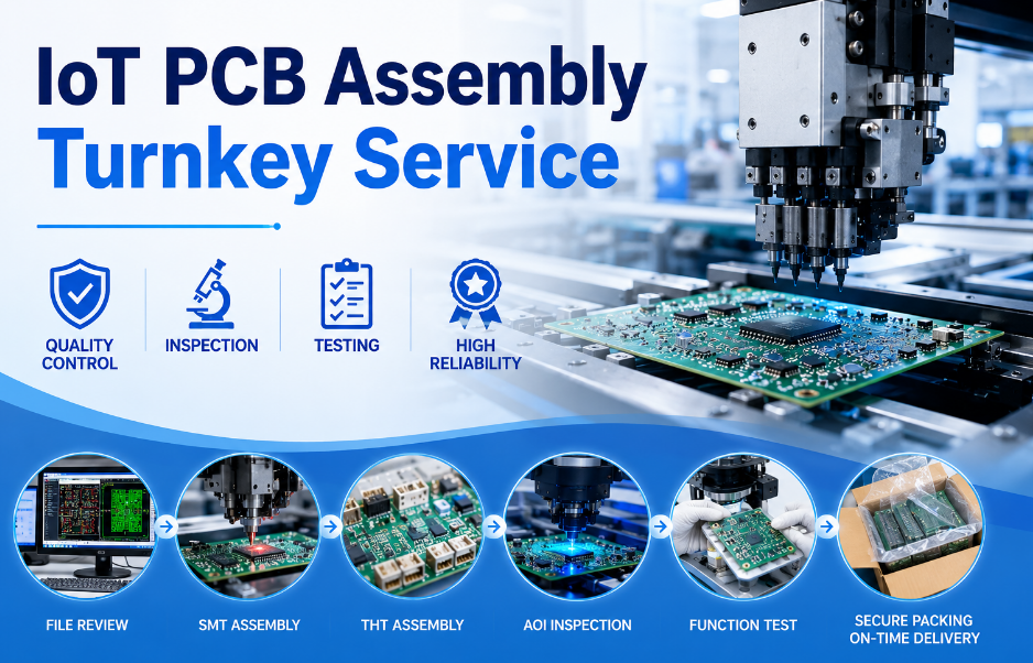
EBest supports robotics PCB manufacturing through PCB design, PCB prototype, mass production, component sourcing, PCB assembly, inspection and testing. This keeps production review, parts preparation, assembly and delivery in one controlled process.
- PCB design and production review
EBest can review Gerber files, BOM, pick-and-place files and assembly drawings before production. This helps check power areas, component spacing, connector positions, test points and assembly risks before the robotics PCB enters fabrication. - PCB prototype for early robot testing
Prototype service helps verify motion control, sensor feedback, robot power PCB stability and AI module function before batch production. Early sample testing can expose voltage drop, signal noise, heat issues or connector risks before the project moves forward. - Component sourcing for BOM control
EBest reviews component availability, package type, lead time and sourcing risk before assembly. This is important for robotics PCB projects that use motor drivers, sensors, wireless modules, AI processors, connectors and high-current power components. - PCB assembly for robot applications
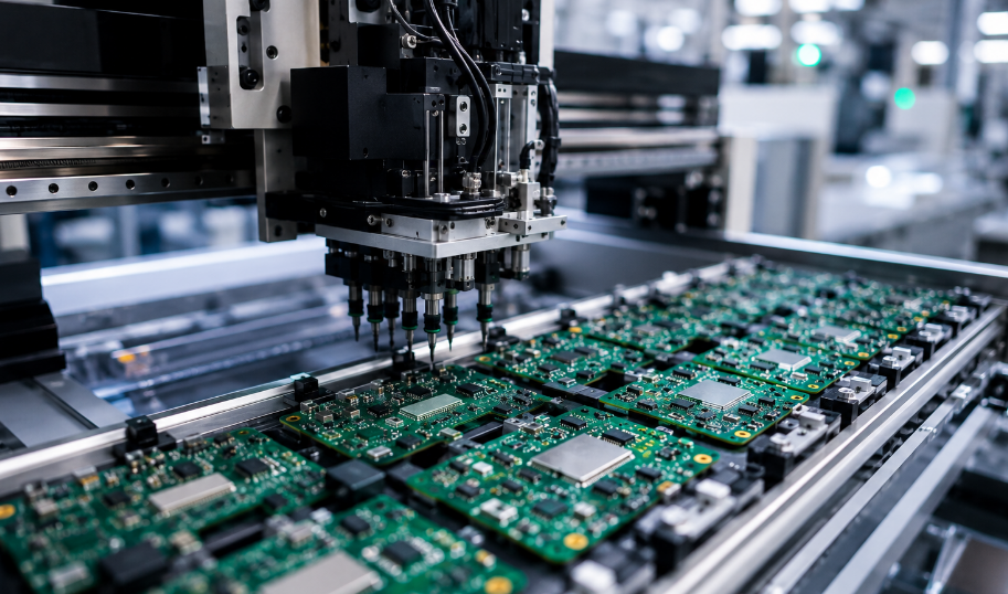
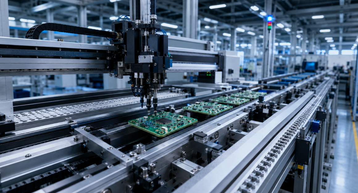
EBest supports SMT assembly, THT assembly and mixed assembly for robotics PCB projects. This fits boards that combine compact ICs, sensors, connectors, terminals, motor driver circuits and power components on one PCBA. - Mass production for repeat orders
After prototype validation, EBest can support small batch, mid-volume robotics PCB assembly and high-volume robotics PCB assembly. Controlled assembly and inspection help keep board quality more consistent across repeat orders. - Inspection and testing before delivery
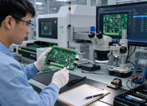
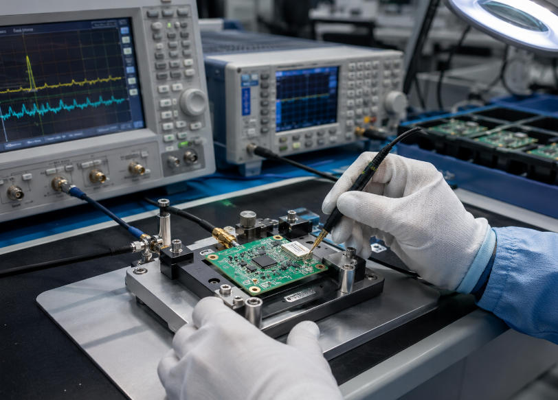
EBest can support AOI inspection, X-ray inspection, electrical testing, power-on testing and functional testing based on project requirements. For robot PCB assembly service, testing should confirm power, signal, communication and key module functions before shipment.
This service flow helps robotics PCB projects move from design files to assembled boards with clearer production control, fewer supplier handoffs and better preparation before batch delivery.
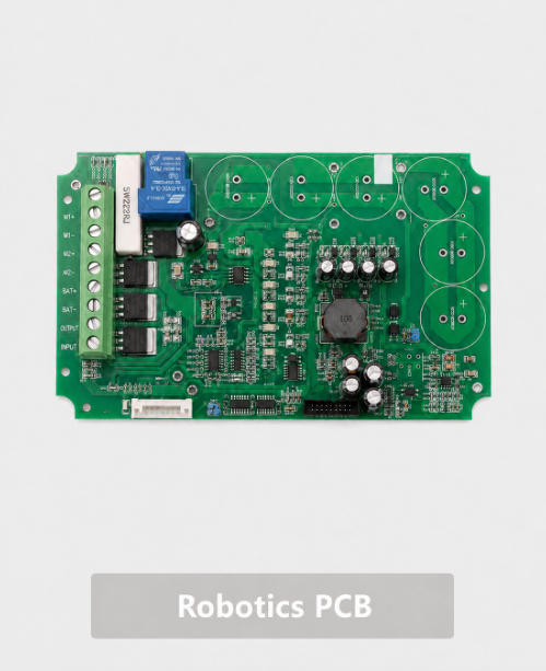
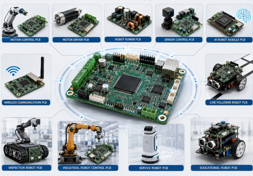
Which Robotics PCB Applications Can EBest Build?
EBest can manufacture and assemble robotics PCBs for motion control, motor drivers, sensor systems, power boards, AI modules, wireless communication and automation equipment. This allows one supplier to support several board types within the same robot project.
Typical robotics PCB applications include:
- Motion control PCB
- Motor driver PCB
- Robot power PCB
- Sensor control PCB
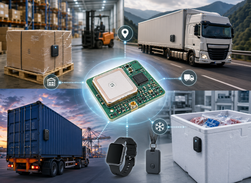
- AI robot module PCB
- AI robotics PCB manufacturing
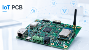
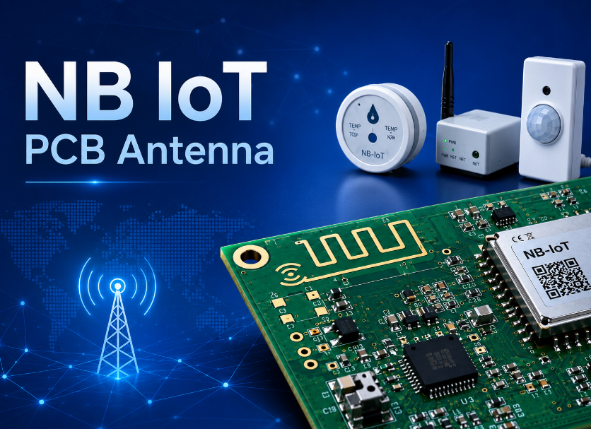
- Wireless communication PCB
- Line follower robot PCB
- Line following robot PCB
- Inspection robot PCB
- Industrial robot control PCB
- Service robot PCB
- Educational robot PCB
These boards often combine power, signal, communication and mechanical stress. As a result, PCB quality, component placement and inspection control directly affect robot operation.
How Does PCB Quality Affect Robot Motion Accuracy?
PCB quality affects robot motion accuracy through power stability, motor driver performance, encoder signal quality, EMI control and assembly consistency. If the motor driver cannot receive stable current, the robot may move with delay, drift or random stop.
Motion control PCB projects usually include drivers, controllers, encoders, connectors and power circuits. When motor EMI affects encoder or control signals, the robot may move incorrectly even when the software logic is right.
For this reason, robotics PCB design should review power trace width, grounding, EMI separation, connector strength and test points before production. During assembly, accurate placement and strong solder joints help keep batch robots performing consistently.
Key review points include:
- Motor control voltage: commonly 5V-48V
- Control signal level: commonly 1.8V-5V
- Encoder signal type: digital or analog
- PCB copper weight: commonly 1oz-3oz
- Test point spacing: commonly 1.0mm-2.54mm
How Do Sensor PCBs Improve Signal Stability in Robots?
Sensor PCBs improve signal stability by supporting clean grounding, low-noise routing, accurate component placement and reliable connector assembly. Stable sensor input helps robots detect objects, follow paths, avoid obstacles and control movement feedback.
In a line follower robot PCB, unstable sensor signals may cause the robot to drift, stop or misread the path. In inspection robots, poor signal quality may affect detection accuracy and response time.
Therefore, sensor PCB production should focus on grounding, connector quality, component polarity and signal integrity. EBest supports PCB in robotics applications where sensor stability must be checked together with assembly quality and testing requirements.
What Makes AI Robotics PCB Assembly More Challenging?
AI robotics PCB assembly is more challenging because AI modules often require stable power, thermal control, high-density SMT placement, camera interfaces and multi-sensor connections. The main risks are high current load, heat concentration, signal interference and hidden soldering defects.
AI robot power PCB projects may place processors, memory, wireless modules, sensors and power circuits in a compact area. If the assembly process is not controlled, BGA, QFN or small-pitch components may create hidden soldering defects.
AI robot testing PCB requirements should go beyond simple power-on checks. The test should confirm power stability, communication, sensor interface, camera connection and module operation before delivery to improve AI robot PCB reliability.
What Should Be Reviewed Before Robotics PCB Production?
Power layout, grounding, EMI control, thermal design, connector placement, component spacing, test points and BOM availability should be reviewed before robotics PCB production. This helps reduce rework before PCB fabrication and assembly begin.
A practical robotics PCB production review should check whether high-current areas are wide enough, whether sensor signals are protected from motor noise, and whether connectors can handle movement and vibration.
BOM review is also important. If key components are obsolete, out of stock or difficult to source, the project may face delay before batch assembly. EBest reviews these risks early so customers can adjust before production.
Production review should cover:
- Power trace width for current capacity and heat control
- Grounding design for signal and power return paths
- EMI control for motor and switching noise reduction
- Thermal layout for drivers, regulators and AI modules
- Connector position for vibration-sensitive areas
- Component spacing for SMT assembly clearance
- Test point access for production testing
- BOM availability for sourcing and lead time control
How Does PCB Assembly Quality Reduce Robotics PCB Failure Risk?
PCB assembly quality reduces robotics PCB failure risk by improving solder joint strength, connector reliability, component placement accuracy and inspection consistency. This is important for robot boards that work under movement, vibration, heat and repeated load changes.
Cold solder joints, insufficient solder, wrong polarity and shifted components may pass simple power-on checks. However, they can cause random failure during long-term robot operation or during system-level testing.
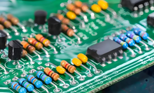
For robotics PCB assembly, SMT precision matters for ICs, sensors and communication modules. THT quality matters for terminals, connectors and power parts. Mixed assembly is useful when one robot board combines compact SMT devices with high-current components.
Assembly risk points include:
- Cold solder joints that cause intermittent failure
- Insufficient solder on high-current pads
- Wrong polarity components that damage power circuits
- Connector solder cracks under vibration
- Shifted components that affect signal or power paths
- Flux residue that may affect long-term reliability
- Batch inconsistency between prototype and repeat orders
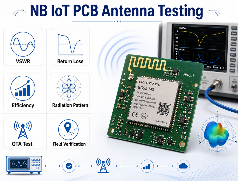
What Tests Are Needed Before Robotics PCB Delivery?
AOI, X-ray inspection, electrical testing, functional testing, power-on testing, thermal review and customized reliability testing may be required before robotics PCB delivery. The final test plan should match the robot’s working environment and board function.
Common robotics PCB tests include:
- AOI inspection for SMT placement and soldering quality
- X-ray inspection for BGA, QFN and hidden solder joints
- Electrical test for open and short circuit checking
- Functional test for power, signal and communication
- Power-on test for basic operating confirmation
- Thermal review for motor drivers, regulators and AI modules
- Connector inspection for vibration-sensitive applications
- Custom robot PCB reliability test based on project requirements
These tests help reduce delivery risk before the robot enters full system testing. For AI robot testing PCB projects, power, signal and communication checks should be confirmed before shipment.
Case Study: Reducing Motion and Sensor Issues Before Batch Production
A robotics PCB project can pass basic power-on testing but still fail during real movement if motor load, sensor noise, vibration and soldering quality are not controlled before batch production. This case shows how production review helps reduce motion and sensor risks before mid-volume assembly.
Project Background
The customer was developing a mobile robot control board for motor control, sensor feedback and power distribution. The prototype could power on, but the board reset when the motor started. During movement testing, the sensor signal also became unstable, which affected motion accuracy and feedback reliability.
Customer Requirements
The project required stable power delivery, lower motor interference, stronger connector soldering, cleaner sensor feedback and consistent PCB assembly quality. The customer also wanted to reduce repeated prototype rework before moving to batch production.
Our Solution
EBest reviewed the Gerber files, BOM, assembly drawing and testing requirements before production. Our team checked high-current power areas, grounding paths, connector positions, component sourcing risks and assembly feasibility. During production, EBest controlled SMT placement, THT soldering, connector assembly, inspection and functional testing.
Output Result
The project moved from prototype validation to mid-volume robotics PCB assembly with lower production risk. The board showed lower reset risk during motor startup, more stable sensor feedback during movement and better consistency before robot system-level testing.
Key results included:
- Lower motion failure risk during motor startup
- More stable sensor feedback during robot movement
- Stronger connector soldering for vibration-sensitive areas
- Better batch consistency before mid-volume production
- Less rework before final robot system testing
- Faster transition from prototype validation to batch assembly
Why Choose EBest for Robotics PCB Manufacturing?
EBest provides PCB fabrication, component sourcing, PCB assembly, testing support and batch production service from one China source factory. For robotics PCB projects, this helps reduce supplier handoff, shorten communication time and lower production risk before delivery.
- One-stop PCB and PCBA service
EBest supports PCB design, PCB prototype, mass production, component sourcing and PCB assembly in one service flow. This keeps board production, parts sourcing and assembly communication in the same production chain. - 20+ years of PCB manufacturing experience
Founded on June 28, 2006, EBest Circuit, also known as Best Technology, has over 20 years of PCB manufacturing experience. This supports robotics PCB production review from prototype verification to stable batch production. - Monthly production capability
EBest’s monthly production capability reaches 260,000 square feet / 28,900 square meters, with more than 1,000 different boards completed monthly. This capacity supports prototype runs, repeat orders, mid-volume robotics PCB assembly and high-volume robotics PCB assembly. - Expedited service for urgent boards
For urgent boards, EBest can provide expedited service, and eligible urgent boards can be shipped within 24 hours when project files, materials and production conditions allow. This is suitable for robotics PCB prototype verification and pilot production schedules. - Wide robotics PCB structure support
EBest supports FR4 PCB, multi-layer PCB, Metal Core PCB, Ceramic PCB, flexible PCB, rigid-flex PCB, RF PCB, High Tg PCB, heavy copper PCB, HDI PCB, high-speed PCB, impedance control PCB and busbar PCB. These options fit robot power PCB, sensor PCB, motion control PCB and AI module PCB requirements. - SMT, THT and mixed assembly capability
EBest supports SMT assembly, THT assembly and mixed assembly for robotics PCB projects. This is important for boards that combine compact ICs, sensors, connectors, terminals and high-current power components. - Certified quality and compliance systems
EBest holds IATF 16949, ISO 9001:2015, ISO 13485:2016, AS9100D, REACH, RoHS and UL. These certifications support process control, material compliance and quality management for global B2B applications. - China source factory with global delivery
EBest does not claim overseas factories, overseas warehouses or local branches. The service is based on China source-factory manufacturing, component sourcing, PCB assembly and global delivery support.
For robotics PCB assembly, EBest supports motion accuracy, sensor stability, AI robot PCB reliability and batch delivery through controlled manufacturing, assembly and testing.

What Files Should You Send for a Robotics PCB Quote?
Send Gerber files, BOM, pick-and-place file, assembly drawing, quantity, testing requirements and special notes about motor load, vibration, heat or working environment for a robotics PCB quote. Complete files help EBest review cost, lead time and production feasibility faster.
Recommended quote files include:
- Gerber file in RS-274X format
- BOM in XLS, XLSX or CSV format
- Pick-and-place file in CSV or TXT format
- Assembly drawing in PDF format
- PCB stack-up if required
- Surface finish requirement
- Order quantity in units or panels
- Testing requirement in PDF or TXT format
- Special notes for motor load, vibration, heat or working environment
If the project includes AI modules, high-current motor drivers or critical sensors, share the test method and operating condition early. This allows a more accurate production review and reduces repeated confirmation before quotation.
FAQs About Robotics PCB Manufacturing
Q1: What is the MOQ for robotics PCB assembly?
A1: The MOQ depends on PCB complexity, component sourcing and testing requirements. For prototype projects, EBest can support small trial orders. For repeat production, mid-volume or high-volume robotics PCB assembly is more suitable after the design, BOM and test process are stable.
Q2: Can EBest source components for robotics PCB assembly?
A2: Yes. EBest can support component sourcing based on the customer’s BOM. Before assembly, the team can review part numbers, package types, availability and lead time risks. For motor drivers, sensors, connectors and AI modules, early BOM review helps reduce production delay.
Q3: What affects the cost of a robotics PCB project?
A3: The main cost factors include PCB layer count, board size, copper weight, surface finish, component quantity, package difficulty, assembly type, testing scope and order volume. BGA, QFN, fine-pitch parts, high-current areas and functional testing can increase the total project cost.
Q4: Should I send a test fixture for robotics PCB functional testing?
A4: If the board requires motion control, sensor feedback, communication or AI module verification, a test fixture is recommended. A fixture helps confirm power, signal and interface functions more consistently before shipment, especially for batch robotics PCB assembly and repeat orders.
Q5: Can EBest handle alternative components if some parts are out of stock?
A5: EBest can help review possible alternative components, but final approval should come from the customer. For robotics PCB projects, replacement parts must match package size, electrical rating, tolerance, temperature range and functional requirements before they are used in production.
Q6: What files are required for faster robotics PCB quotation?
A6: For faster quotation, send Gerber files, BOM, pick-and-place file, assembly drawing, quantity and testing requirements. If the robotics PCB includes motor drivers, sensors, AI modules or high-current circuits, include operating conditions and special inspection notes early.
Q7: Can EBest support both prototype and batch robotics PCB production?
A7: Yes. EBest supports PCB prototype, small batch, mid-volume and high-volume robotics PCB assembly. Prototype production is used for function verification, while batch production focuses on assembly repeatability, inspection control, component supply and delivery consistency.
Q8: What should be confirmed before moving from prototype to batch production?
A8: Before batch production, confirm circuit function, BOM stability, test method, component availability, connector strength, thermal performance and assembly process. For robotics PCB projects, motor load, sensor stability and AI module power behavior should be checked before scaling.
Q9: Can EBest assemble robotics PCBs with both SMT and THT parts?
A9: Yes. EBest supports SMT, THT and mixed assembly. This is useful for robotics PCB projects that combine small ICs, sensors, wireless modules, connectors, terminals and high-current power components on the same board.
Q10: What surface finish is suitable for robotics PCB manufacturing?
A10: Common surface finishes include HASL, lead-free HASL, ENIG and OSP. The right choice depends on component package, soldering requirement, shelf life, cost and reliability needs. For fine-pitch components, BGA or AI module boards, ENIG is often considered during production review.
Q11: How can robotics PCB batch consistency be improved?
A11: Batch consistency can be improved through stable BOM control, clear assembly drawings, approved process settings, AOI inspection, soldering control, functional testing and consistent packaging. For robotics PCB assembly, repeatable production control is important because small defects may affect robot movement or sensor feedback.
Q12: Can EBest support urgent robotics PCB prototype orders?
A12: EBest can provide expedited service for urgent boards when project files, materials and production conditions allow. Eligible urgent boards can be shipped within 24 hours. For faster handling, customers should provide Gerber files, BOM, quantity and assembly requirements at the beginning.
Q13: What certifications does EBest have for PCB manufacturing?
A13: EBest holds IATF 16949, ISO 9001:2015, ISO 13485:2016, AS9100D, REACH, RoHS and UL. These systems support process control, quality management and compliance needs for global B2B PCB projects, including robotics PCB manufacturing and assembly.
Q14: Can a China source factory support overseas robotics PCB projects?
A14: Yes. A China source factory can support overseas robotics PCB projects through custom manufacturing, component sourcing, PCB assembly, testing and global delivery. EBest does not claim overseas factories, overseas warehouses or local branches. The service is based on China source-factory production.
Get a Robotics PCB Quote for Your Project
A reliable robotics PCB should support stable motion, clean sensor feedback, controlled power delivery and tested assembly quality before it enters real robot operation. For motion control boards, sensor boards, AI robot modules and robot power PCB projects, early production review can reduce rework, prevent batch inconsistency and lower delivery risk.
For selection, choose a robotics PCB manufacturer that can review design files, source components, assemble SMT and THT parts, inspect solder quality and support functional testing. For procurement, prepare complete Gerber files, BOM, pick-and-place files, quantity and test requirements before requesting a quote.
EBest Circuit is a China source factory supporting robotics PCB manufacturing and assembly, component sourcing, testing and global delivery for robot projects. Send your Gerber files, BOM, quantity and testing requirements to sales@bestpcbs.com for a robotics PCB manufacturing and assembly quote.