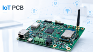
Is your IoT positioning module PCB ready to perform reliably after real deployment? In GPS trackers, GNSS devices, UWB positioning systems, and asset tracking terminals, weak RF performance, unstable power, poor assembly control, or limited testing can quickly turn into signal loss, short battery life, or unstable location data.
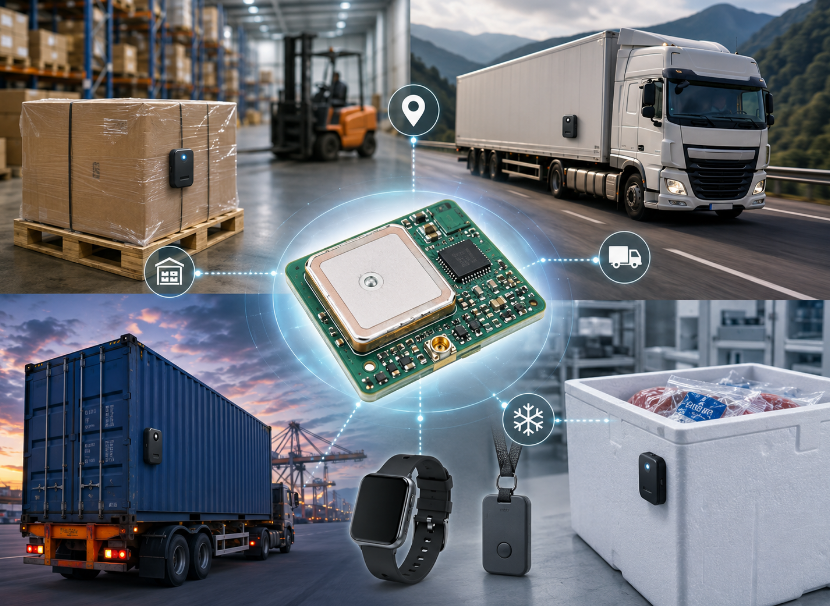
A positioning module board connects location modules, wireless communication circuits, antennas, power management, sensors, and interfaces on one compact PCB. For logistics tracking, vehicle monitoring, industrial equipment, wearable devices, and smart terminals, stable PCB manufacturing and controlled assembly directly affect long-term product performance.
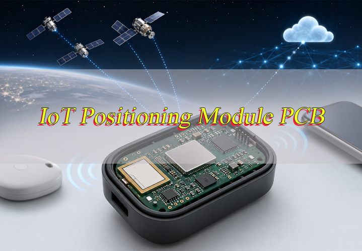
What Is an IoT Positioning Module PCB?
An IoT positioning module PCB is a printed circuit board used in connected devices that collect, process, and transmit location data. It may support GPS, GNSS, UWB, BLE, Wi-Fi, NB-IoT, LTE-M, 4G, LoRa, or several technologies in one product.
This board usually carries the positioning module, wireless module, antenna interface, MCU, memory, power management IC, SIM or eSIM section, sensors, connectors, and test points. Since tracking devices are often compact, the PCB must provide stable RF performance, reliable solder joints, low power operation, and consistent production quality.
IoT tracking PCB products are widely used in asset trackers, vehicle tracking units, smart logistics devices, wearable location products, pet trackers, safety terminals, and industrial IoT equipment. These products may work outdoors, indoors, in motion, or under changing temperatures, so PCB reliability must be considered from prototype to repeated production.
How Does a IoT Positioning Module PCB Work in Tracking Devices?
A positioning module board receives location signals, processes location data, and sends the information to a platform, gateway, or control system. The positioning section collects satellite, wireless, or ranging signals, while the communication section uploads data through the selected network.
For example, a GPS or GNSS tracking unit receives satellite signals through an antenna, calculates position information, and sends the data through NB-IoT, LTE-M, BLE, LoRa, 4G, or another wireless channel. For indoor tracking, UWB or BLE is often used when satellite signals are weak or unavailable.
The PCB supports the signal and power paths behind this process. It connects RF circuits, power rails, interfaces, sensors, and control components, allowing the final device to locate, transmit, and operate reliably. In practice, the board must keep signal loss low, power delivery stable, and assembly accuracy high.
Which Positioning Technologies Are Used in Tracking PCB Products?
Different positioning technologies create different PCB requirements. Some systems focus on wide outdoor coverage, while others focus on indoor accuracy, low power consumption, or long-range data transmission. The right PCB structure depends on the final working environment.
| Technology | Main Use | PCB Focus |
|---|---|---|
| GPS | Outdoor tracking | Antenna access, RF path, power stability |
| GNSS | Multi-satellite positioning | RF sensitivity, shielding, grounding |
| UWB | Indoor high-accuracy positioning | High-frequency signal quality, timing stability |
| BLE | Beacon and short-range tracking | Compact structure, low power operation |
| Wi-Fi | Indoor positioning assistance | RF isolation, module integration |
| NB-IoT | Wide-area low-power tracking | Cellular module support, power control |
| LTE-M | Mobile IoT tracking | Antenna matching, SIM or eSIM interface |
| LoRa | Long-range low-data tracking | RF output, low power operation |
For outdoor asset tracking, GPS, GNSS, NB-IoT, and LTE-M are common choices. For indoor positioning, UWB, BLE, and Wi-Fi assistance are more common. A wireless positioning PCB should be built around the selected technology instead of being treated as a general wireless board.
What Components Are Commonly Used in a Wireless Positioning PCB?
A wireless positioning PCB often combines positioning modules, wireless modules, antennas, MCU units, memory, power management parts, protection components, sensors, and connectors. Each component can affect product stability, assembly yield, and long-term reliability.
Common components include:
- GPS or GNSS module
- UWB transceiver module
- BLE, Wi-Fi, NB-IoT, LTE-M, 4G, or LoRa module
- MCU or application processor
- Ceramic antenna, FPC antenna, PCB antenna, or external antenna connector
- Crystal oscillator or TCXO
- PMIC, LDO, DC-DC converter, and battery charging IC
- SIM card holder or eSIM area
- Accelerometer, gyroscope, temperature sensor, or vibration sensor
- ESD diode, TVS diode, fuse, and surge protection part
- USB, battery, programming, and test connectors
Before assembly starts, footprints, pad sizes, polarity marks, connector orientation, module packages, and test points should be checked carefully. This reduces placement errors and improves production consistency, especially when the PCB includes fine-pitch modules, RF connectors, or compact antenna sections.
How Does RF Performance Affect Tracking Accuracy and Stability?
RF performance directly affects signal reception, communication range, positioning speed, and tracking stability. If the RF path has high loss, poor impedance control, weak grounding, or nearby noise interference, the device may locate slowly, disconnect often, or show unstable position data.
A high-quality tracking PCB should support controlled impedance, short RF paths, clean grounding, proper antenna clearance, and effective EMI control. GPS and GNSS modules work with weak satellite signals, so RF loss and power noise can seriously affect performance. UWB systems also require stable high-frequency behavior because timing accuracy is critical.
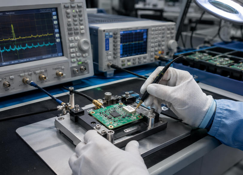
RF performance also affects repeatability in production. A board may pass a simple power-on test but still fail in real tracking conditions. That is why RF-related checks, antenna connection verification, and functional testing should be included before shipment.
How Do GPS, GNSS, UWB, BLE and NB-IoT Affect PCB Performance?
GPS and GNSS need clean RF paths and stable antenna access. These systems rely on weak satellite signals, so grounding, shielding, antenna position, and power noise control all influence final performance. Poor production control can lead to slow signal acquisition or unstable tracking.
UWB focuses more on high-frequency signal quality and timing consistency. It is often used in indoor positioning, warehouse tracking, personnel location, smart access systems, and industrial location products. For UWB positioning PCB products, signal timing, module stability, and RF consistency are key concerns.
BLE and NB-IoT affect the PCB in different ways. BLE supports short-range communication with low power operation, while NB-IoT supports wide-area coverage with low-data transmission. Both require stable power, reliable antenna connection, and clean RF behavior for long-term operation.
What Power Supply Requirements Apply to GPS Tracker PCB Assembly?
Power stability is critical because many positioning devices run on batteries, backup power, solar input, or low-power standby modes. If voltage drops during wireless transmission, the positioning module or communication module may reset, disconnect, or fail to upload data.
A reliable power section should support:
- Stable voltage output for positioning and wireless modules
- Low ripple power rails for RF-sensitive circuits
- Battery charging protection for portable devices
- Sleep and wake-up control for longer operating time
- Surge and ESD protection for external interfaces
- Power path management for battery and external input
For IoT asset tracking PCB assembly, power testing should cover startup behavior, active current, standby current, charging function, and wireless transmission stability. This helps confirm that the finished device remains stable after deployment.
What Materials Are Suitable for Positioning Module PCB Manufacturing?
Material selection affects RF stability, soldering quality, heat resistance, and product reliability. For positioning module PCB manufacturing, materials should match the working frequency, operating environment, product size, and assembly requirements.
- Standard FR-4 Material
FR-4 is suitable for common GPS trackers, BLE tags, logistics trackers, and basic IoT terminals. It offers stable insulation, good mechanical strength, and mature production compatibility. - High-Tg FR-4 Material
High-Tg FR-4 is used for vehicle trackers, outdoor devices, and industrial positioning products. It provides better heat resistance and helps reduce board deformation during assembly and long-term operation. - Halogen-Free FR-4 Material
Halogen-free FR-4 is suitable for products with stricter environmental requirements. It is commonly used in export electronics, wearable devices, and smart hardware. - RF Laminate Material
RF laminate is used for UWB, GNSS, and high-frequency wireless sections. It offers lower signal loss and more stable dielectric performance than standard FR-4. - Rigid-Flex Material
Rigid-flex material is suitable for compact or irregular products. It is often used in wearable trackers, small asset tracking devices, and portable positioning terminals. - Polyimide Flexible Material
Polyimide is used for flexible circuits, antenna connections, and tight internal structures. It provides good flexibility, heat resistance, and mechanical durability. - Copper Foil Material
Copper foil affects current capacity, signal transmission, and heat dissipation. Thicker copper can be used in power, charging, or higher-current sections. - Solder Mask Material
Solder mask protects copper traces from oxidation, moisture, and solder bridging. High-quality solder mask is important for fine-pitch components and module assembly. - Prepreg and Core Material
Prepreg and core materials affect board thickness, insulation, layer bonding, and impedance control. They are important for multilayer tracking PCB production.
For standard tracking products, FR-4 or High-Tg FR-4 is usually enough. For UWB, GNSS, compact wearable, or high-frequency products, RF laminate, rigid-flex material, or polyimide material may be more suitable.
What Surface Finishes Work Best for Tracking PCB Assembly?
Surface finish affects solderability, pad flatness, oxidation resistance, shelf life, and assembly reliability. For tracking PCB assembly, the finish should match the component package, RF requirement, storage condition, and soldering process.
- ENIG Surface Finish
ENIG is commonly used for fine-pitch modules, QFN packages, RF components, antenna connectors, and compact layouts. It provides flat pads, stable solderability, and good oxidation resistance, making it suitable for GPS, GNSS, UWB, and other wireless tracking products. - OSP Surface Finish
OSP is suitable for standard SMT assembly and products with a short storage cycle. It offers a clean copper surface for soldering, but handling and storage should be well controlled because the protective layer is thin. - Immersion Silver Surface Finish
Immersion silver provides good conductivity and can be used for RF-related applications. It is suitable for wireless modules, antenna areas, and communication sections, but proper packaging is important to protect the surface. - Lead-Free HASL Surface Finish
Lead-free HASL offers strong solderability and is suitable for general PCB production with larger pads. For compact tracking products with small packages, it is less common because the surface is not as flat as ENIG. - Immersion Tin Surface Finish
Immersion tin provides a flat surface and can be used for selected connector areas or specific soldering requirements. It requires good storage control to maintain solderability. - Hard Gold Surface Finish
Hard gold is used for contact pads, edge connectors, test points, or repeated mating areas. It is mainly selected for wear-resistant contact surfaces rather than full-board SMT assembly.
For most tracking PCB assembly projects, ENIG is often the preferred option because it supports fine-pitch components, compact structures, RF modules, and stable soldering. OSP, immersion silver, immersion tin, lead-free HASL, or hard gold can be selected based on actual product requirements.
What Should Be Confirmed Before Asset Tracking PCB Assembly?
Clear file preparation helps prevent assembly delays, incorrect placement, and functional failures. Before production, the file package should be reviewed to confirm component orientation, soldering requirements, RF areas, test access, and programming needs.
Key items include:
- Gerber files
- BOM with complete part numbers
- Pick and place file
- Assembly drawing
- Component polarity and orientation notes
- Module footprint confirmation
- RF connector and antenna interface details
- Test points and programming interface
- Firmware loading requirement
- Functional test plan
- Packaging requirement
For IoT module PCB assembly, special attention should be given to RF modules, QFN packages, crystal components, SIM card areas, antenna connectors, battery interfaces, and test points. These areas often determine whether the final tracking device performs consistently.
What Assembly Process Is Used for Tracking PCB Production?
Tracking PCB production requires more than standard SMT mounting. Because the board may include RF modules, fine-pitch ICs, sensors, antenna connectors, power circuits, and SIM/eSIM areas, the process should control solder quality, RF stability, power reliability, and final function.
1. File Review
Review Gerber files, BOM, pick and place files, assembly drawings, and module datasheets. Confirm component polarity, footprint accuracy, RF connector position, antenna interface, test points, and programming method before production.
2. Bare PCB Inspection
Inspect the bare PCB before assembly. Key checks include board thickness, solder mask opening, pad quality, hole accuracy, surface finish, board warpage, copper defects, and impedance requirements for RF-related areas.
3. Component Preparation
Prepare GPS/GNSS modules, UWB modules, BLE or NB-IoT modules, MCU, sensors, connectors, crystals, power ICs, and protection parts. Check part numbers, package types, polarity, moisture sensitivity, and storage condition.
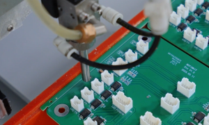
4. Solder Paste Printing
Use a suitable stencil to print solder paste onto PCB pads. Accurate paste control is important for QFN packages, small passive parts, RF components, and module pads to reduce bridging, insufficient solder, and weak joints.
5. SMT Placement
Place resistors, capacitors, ICs, wireless modules, positioning modules, sensors, and connectors by SMT machine. Fine-pitch ICs, RF matching parts, crystal oscillators, antenna connectors, and SIM/eSIM areas require high placement accuracy.
6. Reflow Soldering
Run the PCB through a controlled reflow oven. The temperature profile should match the solder paste, PCB material, and component requirements to reduce tombstoning, solder balls, cold solder, voids, and component shift.
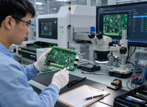
7. AOI and Visual Inspection
Use AOI to check missing parts, wrong parts, polarity errors, solder bridges, insufficient solder, and component offset. Visual inspection is useful for antenna connectors, module edges, SIM areas, battery terminals, and cable interfaces.
8. X-Ray Inspection When Required
Use X-ray inspection for QFN, BGA, LGA, or shielded modules. It helps check hidden solder joints, voids, bridging, insufficient solder, and poor wetting that cannot be seen from the surface.
9. Connector and Cable Assembly
Assemble through-hole connectors, battery holders, antenna cables, USB ports, switches, or external wires if required. Selective soldering, wave soldering, or manual soldering can be used according to the product structure.
10. Cleaning and Surface Check
Check flux residue, solder balls, particles, fingerprints, and surface contamination after soldering. Cleaning is important around fine-pitch parts, RF sections, and high-impedance areas.
11. Programming and Firmware Loading
Load firmware through test pads, USB, UART, SWD, or a custom fixture when required. After programming, confirm that the MCU or communication module starts and communicates correctly.
12. Functional Testing
Test power-on status, current consumption, charging behavior, GNSS response, UWB communication, BLE or NB-IoT connection, sensor output, SIM/eSIM recognition, data transmission, and sleep/wake-up function.
13. RF and Antenna Verification
Check antenna connection, wireless signal response, GNSS reception, UWB ranging, BLE broadcast, or NB-IoT network connection when required. This confirms that the board can support stable tracking performance.
14. Aging Test and Final Inspection
Use aging or burn-in testing to check operating stability when required. Final inspection confirms appearance, labels, connector condition, firmware version, packaging, and test records before shipment.

What Quality Control Supports Wireless Positioning PCB Production?
Quality control should cover incoming materials, PCB fabrication, SMT assembly, soldering quality, electrical function, wireless behavior, and final inspection. For tracking devices, basic electrical testing is not enough because the product must also maintain stable wireless performance.
Important quality controls include:
- IQC inspection for PCB, components, modules, and connectors
- Solder paste inspection for paste volume and print quality
- AOI inspection for placement accuracy and solder defects
- X-ray inspection for QFN, BGA, and hidden solder joints
- ICT testing for short circuits and open circuits
- FCT testing for complete product function
- RF-related checks for wireless signal behavior
- Power testing for voltage, current, charging, and standby mode
- Aging test for long-term operation stability
- Final inspection for appearance, labeling, and packaging
These controls help reduce field failure risk and improve reliability for GPS tracking PCB, GNSS module PCB, UWB positioning PCB, and IoT asset tracking PCB assembly projects.
What Testing Methods Verify Tracking PCB Reliability?
Testing should reflect the final product environment. A wearable tracker, vehicle tracker, logistics tracker, or industrial positioning device may face different operating conditions, so the test plan should match the actual application.
Typical tests include:
- Power-on test
- Current consumption test
- Charging and battery test
- GNSS signal test
- UWB communication test
- BLE or NB-IoT connectivity test
- Firmware programming verification
- Sensor function test
- Antenna connection test
- Temperature cycling test
- Vibration test
- Burn-in or aging test
- Final function test
Outdoor and mobile devices usually require stronger reliability checks. Temperature changes, vibration, battery behavior, connector durability, and wireless stability should be verified before larger production begins.
Where Are IoT Tracking PCB Products Commonly Used?
IoT tracking PCB products are used in location-based devices that collect position data, send status information, and support remote monitoring. These products are common in logistics, mobility, industrial equipment, smart city systems, and personal tracking devices.
Common applications include:
- Asset tracking devices
- Smart logistics trackers
- Vehicle tracking systems
- Fleet management terminals
- Wearable location devices
- Pet tracking devices
- Industrial personnel location systems
- Warehouse UWB positioning products
- Smart city monitoring equipment
- Cold chain tracking devices
- Container and cargo monitoring systems
- Construction equipment tracking units
These applications usually require stable communication, low power operation, compact structure, and reliable PCB assembly. As a result, PCB manufacturing quality and test coverage are just as important as the positioning module itself.
What Problems Affect Tracking PCB Performance and Reliability?
Tracking PCB projects often fail because of small details in RF performance, power stability, antenna connection, soldering quality, or testing coverage. These issues may not appear during a simple power-on check, but they can affect tracking accuracy, communication stability, and field reliability after deployment.
- Weak GPS or GNSS signal reception
Weak signal reception is usually related to antenna connection, RF path loss, poor grounding, nearby noise, or improper shielding. To reduce this risk, the RF path should be kept stable, the antenna interface should be checked, and the GNSS signal response should be tested before shipment. - Slow positioning startup
Some tracking devices take too long to locate because the GNSS module receives poor satellite signals or the antenna area is affected by nearby components. The solution is to review antenna clearance, module power supply, crystal stability, and RF connection. - Unstable BLE, UWB, or NB-IoT connection
Wireless connection may become unstable when the module has weak solder joints, poor antenna matching, power noise, or interference from nearby circuits. The practical solution is to verify module placement, antenna connection, power rail stability, and communication function during assembly testing. - High standby current and short battery life
High power consumption often comes from leakage current, wrong component status, incomplete sleep mode, or unstable firmware settings. To solve this, current should be measured in startup, working, transmission, sleep, and charging modes. - Module reset during wireless transmission
Positioning or communication modules may reset when current peaks occur during data transmission. The solution is to check voltage drop, capacitor selection, battery input, charging circuit behavior, and peak current support under real communication conditions. - Poor soldering on fine-pitch parts
QFN packages, small passive components, RF matching parts, and module pads may suffer from bridging, insufficient solder, voids, or placement offset. This can be reduced by controlling stencil opening, solder paste printing, SMT placement accuracy, reflow profile, AOI inspection, and X-ray inspection. - SIM, eSIM, antenna, or connector failure
SIM holders, antenna connectors, USB ports, battery terminals, and cable interfaces may fail because of weak soldering, wrong orientation, or mechanical stress. The solution is to confirm connector direction, pad strength, solder fullness, plug-in force, and final appearance before shipment. - Inconsistent performance between samples and batch production
A sample may work well, but batch production may show different RF performance, soldering quality, or current consumption. To avoid this, the project should use confirmed materials, stable process settings, inspection records, and repeatable functional tests.
How to Choose a Reliable IoT Positioning Module PCB Manufacturer?
Choosing a reliable tracking PCB manufacturer should focus on production control, assembly capability, RF awareness, testing support, and communication efficiency. A good manufacturer should not only make the bare PCB, but also help reduce risks in module assembly and product verification.
- Check experience with wireless and positioning products
The manufacturer should have experience with GPS, GNSS, UWB, BLE, NB-IoT, LTE-M, LoRa, and other wireless module PCB projects. This experience helps with RF areas, antenna connectors, module soldering, SIM/eSIM interfaces, and wireless function testing. - Confirm complete PCB manufacturing and assembly support
A reliable partner should support PCB fabrication, SMT assembly, component preparation, soldering inspection, programming, functional testing, and final inspection. This helps keep production details in one controlled process and reduces mistakes between different suppliers. - Review material and surface finish options
Tracking products may use FR-4, High-Tg FR-4, RF laminate, rigid-flex material, ENIG, OSP, immersion silver, or other options. The manufacturer should recommend suitable materials and finishes based on RF performance, soldering quality, operating environment, and product structure. - Check fine-pitch and module assembly capability
Many positioning boards include QFN packages, LGA modules, small passive components, RF matching parts, antenna connectors, and compact sensor areas. The manufacturer should have controlled solder paste printing, accurate SMT placement, stable reflow soldering, AOI inspection, and X-ray inspection when required. - Ask about power and RF-related testing
Basic electrical testing is not enough for wireless positioning PCB production. Useful tests may include current consumption, charging behavior, GNSS response, UWB communication, BLE broadcast, NB-IoT connection, antenna check, sleep/wake-up mode, and functional data transmission. - Evaluate file review before production
Gerber files, BOM, pick and place files, assembly drawings, module datasheets, polarity notes, and test requirements should be reviewed before production starts. A reliable manufacturer will confirm unclear details early to avoid wrong components, wrong orientation, missing test points, or poor assembly results. - Look for stable repeat production control
For repeated orders, the manufacturer should maintain material consistency, process parameters, soldering standards, inspection records, and test results. This is important for GPS tracking PCB, GNSS module PCB, UWB positioning PCB, and asset tracking PCB assembly projects.
Why Choose EBest for IoT Positioning Module PCB Manufacturing?
EBest supports IoT positioning module PCB manufacturing and assembly for GPS trackers, GNSS devices, UWB positioning systems, BLE beacons, NB-IoT trackers, asset tracking terminals, and wireless location products. The service focuses on stable quality, reliable assembly, practical testing, and smooth project coordination.
- One-stop PCB manufacturing and assembly support
EBest supports PCB fabrication, SMT assembly, component preparation, soldering inspection, programming, functional testing, and final delivery support. This helps keep the full production process easier to manage and reduces avoidable communication gaps. - Experience with tracking and wireless module products
EBest works with communication PCB, wireless module PCB, tracking device PCB, IoT PCB assembly, and asset tracking PCB projects. This experience is useful for products that include GPS/GNSS modules, UWB modules, BLE modules, NB-IoT modules, antennas, sensors, power circuits, and compact connectors. - Controlled assembly for compact modules
IoT positioning module PCB products often include QFN packages, RF matching components, crystal oscillators, antenna connectors, SIM/eSIM sections, and small module areas. EBest supports controlled SMT placement, reflow soldering, AOI inspection, visual inspection, and X-ray inspection when required. - Testing support for real operating functions
EBest can support power-on checks, current consumption testing, charging function checks, firmware programming, functional testing, antenna connection checks, RF-related verification, and aging tests based on project requirements. This helps confirm that the assembled PCB is ready for real tracking use. - Flexible material and finish selection
EBest can support common materials and surface finishes such as FR-4, High-Tg FR-4, RF-related materials, rigid-flex structures, ENIG, OSP, immersion silver, and other options. This makes it easier to match different tracking applications and production requirements. - Clear communication from sample to batch production
EBest helps review files, confirm component details, check assembly requirements, and support testing before production. This reduces preventable errors and supports smoother production for IoT positioning module PCB projects. - Customized support for different tracking applications
Whether the product is used for asset tracking, vehicle tracking, smart logistics, indoor UWB positioning, wearable tracking, cold chain monitoring, or industrial IoT equipment, EBest can provide customized PCB manufacturing and assembly support based on the actual project requirements.
FAQs About IoT Positioning Module PCB
Q1: What should be checked first when a tracking device has weak positioning performance?
A1: Start with the antenna connection, RF path, grounding, module power supply, and GNSS signal response. Weak positioning is often caused by RF loss, unstable power, poor antenna contact, or interference near the wireless section.
Q2: Why does a tracking PCB consume too much power?
A2: High power consumption may come from leakage current, incomplete sleep mode, wrong component status, unstable firmware, or excessive transmission current. Current testing should cover startup, active tracking, wireless transmission, charging, standby, and sleep modes.
Q3: How can batch quality remain stable after the sample is approved?
A3: Stable batch quality depends on confirmed materials, fixed surface finish, controlled SMT parameters, clear inspection standards, and repeatable functional testing. Test records should also be kept for production traceability.
Q4: Which parts of a GPS tracker PCB require extra assembly attention?
A4: RF modules, GNSS modules, UWB modules, QFN packages, antenna connectors, crystal oscillators, SIM/eSIM areas, battery terminals, and test pads require extra attention. These areas often affect signal stability, soldering reliability, and final function.
Q5: Is a power-on test enough for asset tracking PCB assembly?
A5: No. A power-on test only confirms that the board can start. A stronger test plan should include current consumption, charging behavior, GNSS response, wireless connection, antenna status, sensor output, firmware function, and sleep/wake-up behavior.
Q6: What files make production review faster?
A6: Gerber files, BOM, pick and place file, assembly drawing, module datasheets, polarity notes, test plan, firmware instructions, and packaging requirements help speed up review and reduce production mistakes.
How Can You Start Your IoT Positioning Module PCB Project with EBest?
Ready to start your IoT positioning module PCB project? EBest provides IoT PCB manufacturing, PCB assembly, component support, functional testing, and delivery coordination for GPS, GNSS, UWB, BLE, NB-IoT, and asset tracking applications.
Send your Gerber files, BOM, placement file, assembly drawing, module datasheets, and test requirements to sales@bestpcbs.com. EBest will review your project and support you with customized manufacturing, stable assembly quality, reliable testing, and professional follow-up from sample build to repeated production.