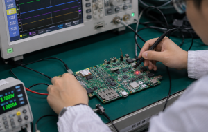
Is IoT module PCB assembly slowing your smart device project? A smart device may look simple from the outside, but the PCB inside must handle power control, wireless communication, signal stability, data processing, and long-term operation at the same time.
That is why IoT module PCB assembly should be planned carefully from the first sample stage. A stable assembly process helps reduce production problems, improve product reliability, and make repeat orders easier to control.
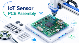
What Is IoT Module PCB Assembly?
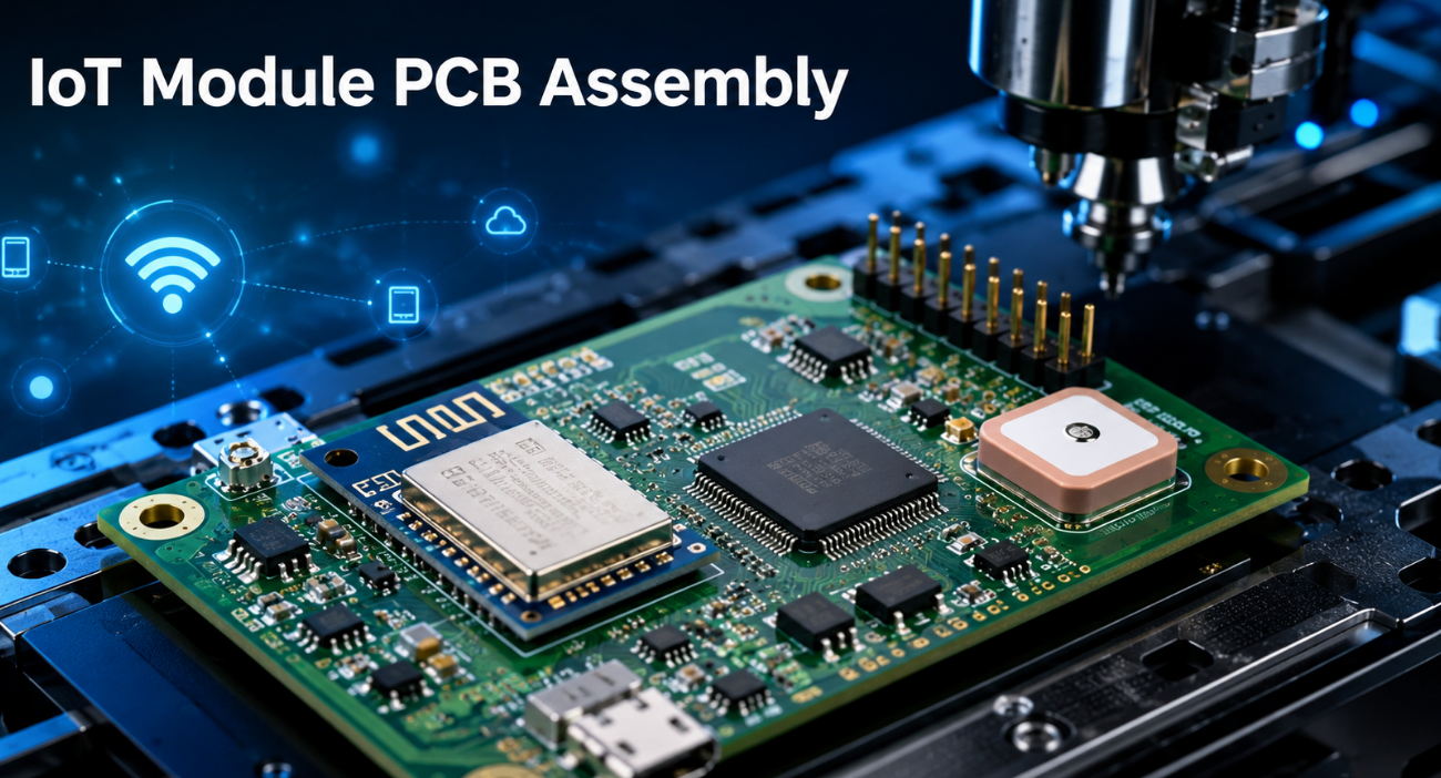
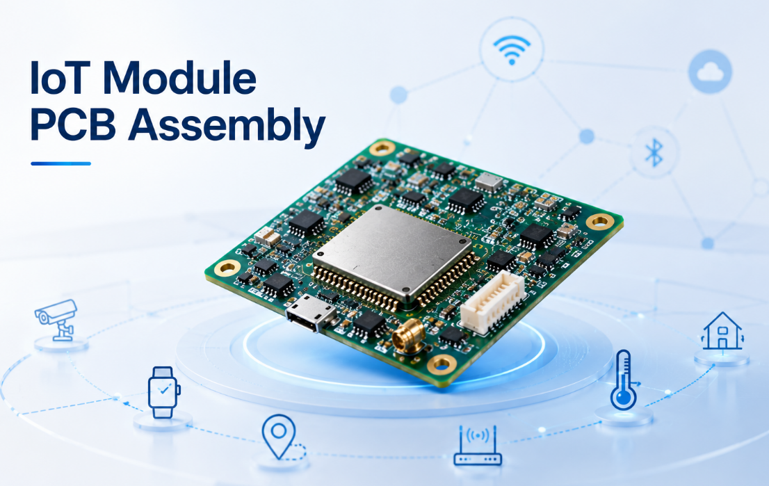
IoT module PCB assembly is the process of mounting electronic components onto PCB boards used in smart connected devices. These boards usually include wireless modules, GPS modules, sensors, control chips, power circuits, connectors, antennas, shielding parts, and power interfaces.
The PCB works as the main connection platform of the device. After components are assembled onto the board, the device can collect data, send signals, receive commands, track location, and work in real operating conditions.
A complete IoT module PCB assembly service usually includes:
- PCB fabrication for board structure, layer count, copper weight, solder mask, and surface finish
- Component sourcing based on BOM, package, part number, and supply availability
- SMT assembly for ICs, wireless modules, sensors, and passive components
- Through-hole assembly for connectors, terminals, pin headers, and mechanical parts
- Shielding assembly for GPS, RF, wireless, and EMI-sensitive areas
- Inspection and functional testing before shipment
- Cleaning, labeling, packaging, and delivery support
For products using Bluetooth, WiFi, LoRa, NB-IoT, LTE-M, GPS, GNSS, or other wireless functions, assembly quality can affect signal strength, battery life, connection stability, and final product performance.
What Smart Devices Use IoT Module PCB Assembly?
Many smart devices use IoT module PCB assembly because they rely on wireless communication, sensing, tracking, or remote control. These devices are usually compact, but the PCB inside must support several functions at once.
Common applications include:
- GPS trackers: Used for vehicle tracking, asset tracking, fleet management, personal location devices, and anti-theft products.
- Smart meters: Used in electricity meters, water meters, gas meters, and energy monitoring systems.
- Industrial sensors: Used for temperature, pressure, vibration, humidity, motion, and equipment status monitoring.
- Smart home controllers: Used in lighting control, door locks, HVAC systems, alarms, and appliance control.
- Wearable devices: Used in health monitoring, sports tracking, portable electronics, and personal safety devices.
- Wireless gateways: Used to collect data from sensors and send it to cloud platforms or control systems.
- Medical monitoring terminals: Used in portable medical devices, remote monitoring equipment, and connected healthcare products.
- Security devices: Used in access control systems, alarms, surveillance terminals, and smart entry devices.
- Vehicle tracking units: Used in logistics, fleet systems, shared mobility, and transportation monitoring.
In these products, the PCB board is more than a carrier for components. It manages power, sensors, wireless communication, signal transmission, and cloud connection.
Why Do IoT Modules Require Reliable PCB Assembly?
IoT modules require reliable PCB assembly because they often run continuously and communicate wirelessly in real environments. Some devices are installed outdoors, inside machines, in vehicles, or in locations where repair is difficult.
Main reasons include:
- Long working time: Many IoT devices run day and night, so weak solder joints or unstable components may cause failure over time.
- Wireless dependence: Poor assembly may reduce signal strength, connection range, data transmission, or GPS positioning.
- Compact board space: Small layouts make component placement, soldering, and inspection more sensitive.
- Field operation: Devices may face vibration, heat, humidity, dust, unstable voltage, or battery power changes.
- Repair difficulty: Once a device is installed, replacement or rework can cost more than proper assembly control.
- Batch consistency: Repeat orders should perform the same as approved samples, especially when products are shipped in volume.
Reliability starts from small production details. Solder paste printing, SMT placement, reflow temperature, polarity checking, board cleaning, inspection, and testing all influence the final result.
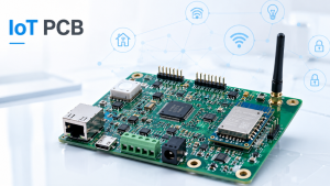
What Components Are Commonly Used in IoT Module PCB Boards?
IoT module PCB boards use many small and functional components. Each part has a clear job, and all parts must work together after assembly.
Common components include:
- MCU or processor: Controls data processing, system logic, device operation, and communication commands.
- Wireless module: Supports Bluetooth, WiFi, Zigbee, LoRa, NB-IoT, LTE-M, 4G, or other communication functions.
- GPS/GNSS module: Provides positioning, navigation, tracking, and location data.
- SIM card slot or eSIM interface: Used for cellular IoT products with mobile network access.
- Antenna connector: Connects internal or external antennas for GPS, cellular, WiFi, or LoRa functions.
- Crystal oscillator: Supports stable timing for communication modules and control circuits.
- Power IC: Manages voltage conversion, charging, protection, and stable power supply.
- Sensors: Collect temperature, pressure, motion, humidity, light, vibration, or other data.
- Passive components: Include resistors, capacitors, inductors, diodes, filters, and protection parts.
- Connectors and terminals: Support power input, data connection, programming, debugging, and external interfaces.
- Shielding cover: Helps reduce EMI and protect sensitive RF or wireless areas.
- Battery interface: Supports portable, low-power, rechargeable, or backup-power IoT products.
- LED indicator or buzzer: Provides basic status indication, alarm signals, or device feedback.
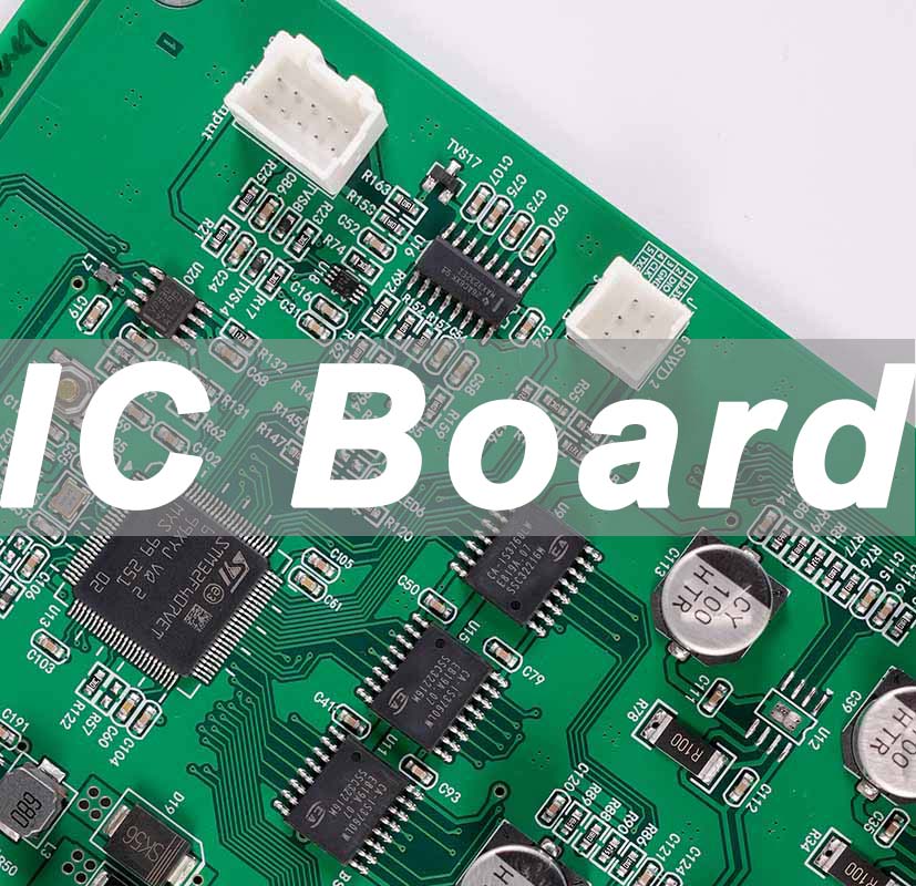
Many IoT boards use fine-pitch packages such as QFN, BGA, LGA, DFN, and small passive components like 0201 or 0402. These parts require accurate SMT placement, proper stencil control, stable reflow soldering, and careful inspection.
What Wireless Functions Should an IoT Module PCB Support?
An IoT module PCB should support wireless functions based on working distance, power consumption, data rate, and application environment. Different wireless technologies bring different assembly and testing requirements.
Common wireless functions include:
- Bluetooth: Used for short-range connection in wearables, sensors, smart locks, and portable devices. It is often used when the device works close to a phone, gateway, or control terminal.
- WiFi: Used for smart home devices, gateways, cameras, and control terminals. It supports higher data speed but requires stable power and a good antenna connection.
- Zigbee: Used for low-power mesh networking in smart control systems, lighting, and home automation. It is suitable for devices that work together in a local network.
- LoRa: Used for long-distance, low-power communication in remote sensors, meters, and outdoor IoT devices. It is useful when the device sends small amounts of data over a long distance.
- NB-IoT: Used for smart meters, parking systems, and remote monitoring devices. It is suitable for low-data applications that require wide network coverage.
- LTE-M: Used for tracking devices, wearables, and products that move between locations. It supports better mobility and faster response than many low-power cellular options.
- GPS/GNSS: Used for positioning and navigation in tracking devices, fleet systems, and location-based equipment. It requires careful antenna placement, clean RF assembly, and stable power supply.
- UWB: Used for high-accuracy location and distance measurement in indoor positioning and asset tracking. It is useful when precise location data is required.
- RFID: Used for identification and short-distance data reading in access control, inventory, and tracking systems.
Wireless sections are sensitive to assembly quality. Poor soldering, wrong module direction, weak shielding, poor antenna connection, or contamination around RF areas may reduce signal strength and make communication unstable.
How Does GPS Affect IoT Module PCB Assembly?
GPS affects IoT module PCB assembly because GPS signals are weak when they reach the device. The PCB must help receive, protect, and process these signals with as little interference as possible.
For an IoT GPS module PCB assembly service, the following points should be controlled carefully:
- Antenna placement: The GPS antenna area should avoid strong noise sources, metal blocking, and crowded component areas.
- RF path stability: RF-related components should be placed accurately and kept clean to reduce signal loss.
- Grounding quality: Good grounding helps reduce noise and improve GPS signal behavior.
- Shielding control: Shielding covers should be assembled properly to protect sensitive GPS and RF areas.
- Power stability: Stable voltage helps the GPS module start faster and locate more reliably.
- Connector assembly: Antenna connectors must be soldered firmly and positioned correctly.
- Module orientation: GPS modules should follow the assembly drawing to avoid placement errors.
- Post-assembly testing: GPS signal response should be checked when location performance is important.
Small assembly errors may cause slow positioning, unstable tracking, signal loss, or repeated module restart. That is why GPS-related IoT boards should not rely only on simple power-on checks.
What Should Be Confirmed Before IoT Module PCB Assembly Starts?
Before IoT module PCB assembly starts, all production files and project requirements should be clear. Good preparation helps reduce quotation delays, material mistakes, assembly problems, and repeated communication.
The basic file package should include:
- Gerber files for PCB fabrication
- BOM with clear part number, value, package, quantity, tolerance, and approved alternatives
- Pick and place file for SMT component placement
- Assembly drawing for orientation, polarity, connector direction, and special notes
- PCB specification for material, thickness, copper weight, surface finish, solder mask, and layer count
- Testing instructions for power, communication, GPS, sensor, and functional checks
- Firmware notes if programming, startup testing, or firmware loading is required
- Packaging requirements for labeling, anti-static packing, tray packing, or carton marks
For wireless or GPS products, extra information is helpful:
- Antenna type and antenna position
- Wireless module model
- RF test requirements
- Shielding request
- Power consumption target
- Battery or charging requirements
- Connector direction and mechanical clearance
- Final working environment
- Expected production volume and delivery schedule
For repeat orders, approved sample records, test standards, material changes, and previous production notes should also be confirmed. This helps keep the new batch consistent with the earlier approved version.
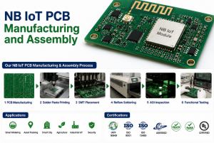
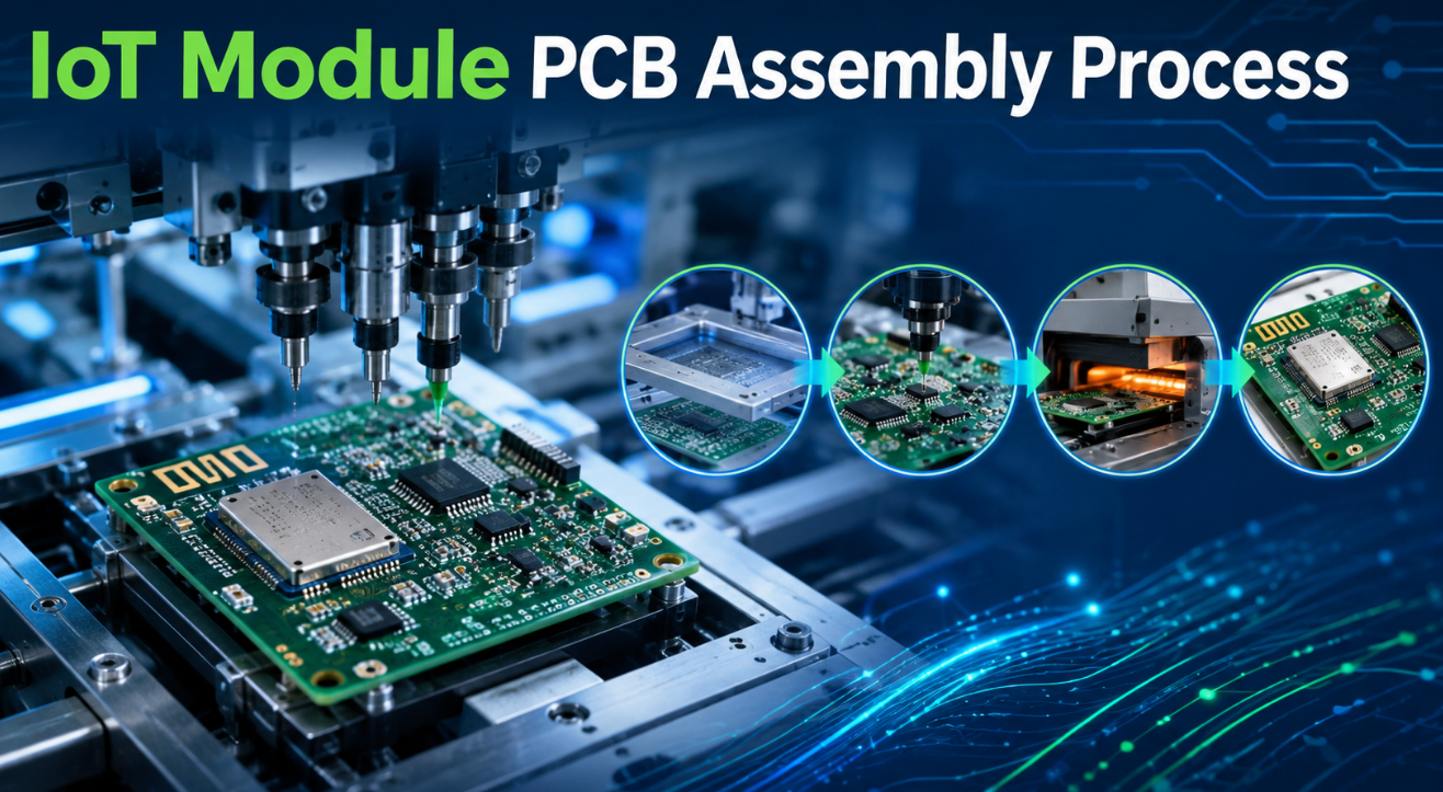
What Is the Standard IoT Module PCB Assembly Process?
The standard IoT module PCB assembly process should be clear and controlled from file review to final shipment. Each step affects the next step, so missing details at the beginning may create problems later.
1. File review
Gerber files, BOM, placement data, assembly drawings, and test notes are checked first. This step helps find missing files, unclear polarity, footprint mismatches, special soldering notes, and possible production risks.
2. PCB fabrication
The PCB is produced according to the required material, layer count, board thickness, copper weight, solder mask, silkscreen, and surface finish. For compact IoT boards, pad quality and solder mask accuracy are important.
3. Component sourcing
Part number, package, quantity, lead time, and substitute options are checked carefully. Reliable sourcing helps avoid wrong parts, unstable supply, or last-minute delays before SMT production.
4. Solder paste printing
Solder paste is printed onto the PCB pads through a stencil. Paste thickness, opening size, and printing alignment affect solder joint quality, especially for QFN, BGA, LGA, and small passive components.
5. SMT placement
SMT machines place ICs, wireless modules, sensors, resistors, capacitors, connectors, and other surface-mounted parts onto the board. Accurate placement is important for fine-pitch components and RF-related parts.
6. Reflow soldering
The boards pass through reflow soldering, where solder paste melts and forms solder joints between the components and PCB pads. A proper reflow profile helps improve solder strength and reduce defects.
7. Inspection after reflow
AOI, X-ray, visual inspection, and functional checks may be used to check component position, polarity, solder bridges, missing parts, voids, and hidden soldering issues.
8. Secondary assembly
Through-hole parts, shielding covers, special connectors, mechanical parts, wires, or terminals are assembled after SMT when required. This step should follow clear assembly drawings and handling instructions.
9. Testing and packing
The boards go through functional testing, cleaning, labeling, anti-static packing, and shipment preparation based on project requirements. Test records and packing labels can also be arranged when required.
How Can Signal Stability Be Improved During PCB Assembly?
Signal stability can be improved during PCB assembly by controlling component placement, soldering quality, RF areas, grounding points, shielding parts, and connector assembly. For IoT boards, these small details often decide real performance.
Key control points include:
- Accurate RF component placement: Antenna connectors, GPS modules, wireless modules, crystals, filters, and matching components should follow the placement file closely.
- Stable soldering quality: Solder bridges, voids, cold joints, poor wetting, and weak solder points should be avoided because they may affect signal transmission.
- Clean RF area: Flux residue, dust, contamination, or poor cleaning may affect sensitive signal areas.
- Proper shielding assembly: Shielding covers should be placed firmly and correctly to reduce interference.
- Reliable grounding: Weak ground connection may allow noise to enter wireless sections and lower signal stability.
- Correct connector direction: Antenna, communication, and power connectors should match the assembly drawing.
- Controlled power noise: Power circuits should be assembled and tested carefully because unstable voltage may affect wireless startup.
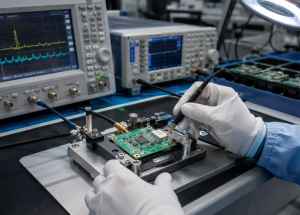
- Functional signal testing: Communication testing, GPS signal testing, and RF-related checks help confirm real performance.
For wireless products, power-on checks alone are not enough. A board can turn on normally but still have weak GPS reception, unstable Bluetooth pairing, poor WiFi response, or poor cellular startup.
Signal stability should be checked according to the product function. For example, a GPS tracker should focus on positioning response, while a gateway board may focus more on communication range and stable data transmission.
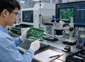
What Quality Tests Are Needed for IoT Module PCB Assembly?
Quality tests for IoT module PCB assembly should confirm both assembly quality and product function. The goal is to find problems before the boards are shipped, not after they enter final products.
| Test Method | Purpose |
|---|---|
| AOI | Checks placement, polarity, missing parts, and visible solder defects |
| Visual Inspection | Confirms appearance, component direction, connectors, labels, and obvious defects |
| X-ray | Checks hidden joints under BGA, QFN, LGA, and similar packages |
| ICT | Checks basic electrical connection and component values |
| Flying Probe Test | Supports electrical testing for prototypes and low-volume boards |
| Functional Test | Confirms whether the board works under real operating conditions |
| Power Test | Checks voltage, current, startup behavior, charging behavior, and power stability |
| Communication Test | Checks WiFi, Bluetooth, LoRa, NB-IoT, LTE-M, cellular, or other wireless functions |
| GPS Signal Test | Checks positioning behavior, module response, and signal reception |
| RF Test | Confirms RF-related performance when required |
| Firmware Programming Test | Confirms whether the board can be programmed and started correctly |
| Aging Test | Helps find unstable faults before shipment |
For IoT devices, testing should match the final product function. A smart meter, GPS tracker, sensor board, and wireless gateway may require different test plans.
A good test plan should be confirmed before assembly starts. This allows test fixtures, test firmware, power settings, and acceptance standards to be prepared in advance.
What Problems Often Happen in IoT Module PCB Assembly Projects?
Problems in IoT module PCB assembly often come from unclear files, wrong components, poor soldering, unstable signal behavior, and insufficient testing. These problems can delay production and increase rework cost.
Common problems include:
- Incomplete BOM information
The BOM should include clear part number, value, package, tolerance, quantity, and approved alternatives. Missing information may lead to sourcing errors or wrong substitutes. - Wrong component package
A part may have the correct value but the wrong footprint. This can stop SMT production or cause poor soldering results. - Poor soldering control
Open joints, solder bridges, tombstoning, voids, and weak solder joints are common risks on fine-pitch ICs, QFN packages, and small passive components. - Unstable wireless or GPS performance
Antenna interference, weak grounding, shielding problems, incorrect connector assembly, contamination, or poor soldering around RF parts may affect signal behavior. - Insufficient functional testing
Hidden issues may pass into shipment if only appearance checks are performed. Wireless, GPS, power, and sensor functions should be checked according to the product. - Unclear assembly notes
Connector direction, module orientation, shielding position, polarity marks, and special handling instructions should be shown clearly in the assembly drawing. - Material supply changes
Unapproved substitute parts may change power behavior, signal performance, product stability, or certification-related requirements. - Weak packaging control
Poor anti-static protection, loose packing, or unclear labels may cause damage, confusion, or extra checking after delivery.
Most of these problems can be reduced before production starts. Clear files, BOM checking, sample confirmation, DFM review, and suitable testing can prevent many avoidable delays.
How to Choose an IoT Module PCB Board Manufacturer?
Choosing an IoT module PCB board manufacturer should focus on capability, communication, process control, testing support, and delivery stability. Basic PCB production is not enough for complex IoT products.
Important selection points include:
- One-stop service capability
The manufacturer should support PCB fabrication, component sourcing, SMT assembly, through-hole assembly, inspection, testing, and packing. This reduces coordination risk. - IoT assembly experience
Experience with GPS modules, RF parts, wireless modules, fine-pitch components, sensors, shielding covers, and compact PCB structures is important. - Component sourcing control
The team should check part number, package, lead time, availability, approved alternatives, and material traceability before production. - SMT process capability
Fine-pitch ICs, QFN, BGA, LGA, DFN, and 0201 or 0402 components require stable SMT placement and soldering control. - Testing support
The manufacturer should support functional testing, communication testing, GPS testing, power testing, firmware programming, and other project-specific checks. - Prototype and batch support
Support for samples, small batches, and repeat orders makes the project easier to scale without changing partners too often. - Clear communication
Fast file review, risk feedback, practical suggestions, and stable delivery updates help reduce project uncertainty. - Delivery management
Lead time, material schedule, production plan, and shipment preparation should be communicated clearly before order confirmation.
A good manufacturer should review files before production, point out possible risks, and provide practical solutions. This type of support is more valuable than simply assembling boards without checking details.
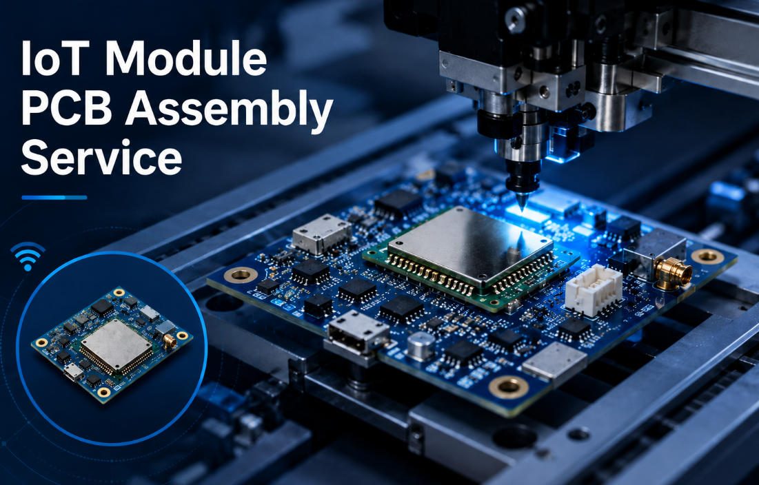
Why Choose EBest for IoT Module PCB Assembly Service?
EBest provides IoT module PCB assembly service for smart devices, GPS tracking products, wireless modules, sensors, gateways, security terminals, and connected electronic equipment. Here are reasons why choose us for IoT module PCB assembly manufacturer:
- PCB fabrication for different board structures and specifications
- Component sourcing based on BOM and approved part numbers
- SMT assembly for fine-pitch ICs, wireless modules, sensors, and compact components
- Through-hole assembly for connectors, terminals, pin headers, and special parts
- RF-related assembly support for GPS, GNSS, wireless module, and antenna-related boards
- Shielding cover assembly for EMI-sensitive and RF-sensitive areas
- Inspection and functional testing according to project requirements
- Prototype, small batch, and repeat production
- Delivery support with clear packing and shipment preparation
For IoT projects, EBest focuses on accurate SMT placement, stable soldering, RF-related assembly support, flexible production volume, and clear project communication.
FAQs About IoT Module PCB Assembly
Q1: Can EBest sign an NDA before reviewing project files?
A1: Yes. EBest can support NDA review before file discussion. This helps protect product drawings, BOM details, firmware notes, test methods, and project-related business information.
Q2: Can EBest help check whether a project is suitable for prototype or direct batch production?
A2: Yes. EBest can review the project stage and suggest whether sample verification, pilot production, or batch production is more suitable based on board complexity and delivery goals.
Q3: Can assembled IoT module PCB boards be packed by project or version number?
A3: Yes. EBest can arrange labels, version marks, anti-static bags, trays, cartons, and shipment notes according to project requirements. Clear packing helps reduce mixing risk after delivery.
Q4: Can EBest support partial turnkey and full turnkey cooperation?
A4: Yes. EBest can support both options. For partial turnkey, some materials can be supplied by the project side. For full turnkey, EBest can handle PCB production, material sourcing, assembly, and delivery support.
Q5: Can EBest handle urgent IoT module PCB assembly orders?
A5: Urgent orders can be reviewed based on material availability, board complexity, testing requirements, and current production schedule. Early file sharing helps improve the chance of faster scheduling.
Q6: Can EBest keep production records for future repeat orders?
A6: Yes. EBest can keep important production references such as approved BOM, PCB version, assembly notes, packing method, and test requirements to support smoother repeat production.
Q7: Can EBest support small design changes between two production batches?
A7: Yes. If a new PCB version, BOM update, connector change, or module replacement is required, EBest can review the change before production to reduce version mismatch and assembly risk.
How Can You Start an IoT Module PCB Assembly Project?
Starting an IoT module PCB assembly project with EBest is simple. Prepare the Gerber files, BOM, pick and place file, assembly drawing, and test requirements, then send the project details for review.
To start faster, prepare:
- Gerber files
- BOM
- Pick and place file
- Assembly drawing
- Testing requirements
- Target quantity
- Expected delivery schedule
- Special notes for GPS, wireless, RF, shielding, or firmware functions
Send your files and project requirements to sales@bestpcbs.com. EBest will review your project, provide a practical assembly solution, and offer a fast quotation for your IoT PCB assembly project.