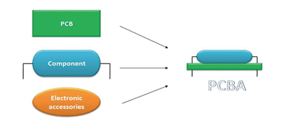
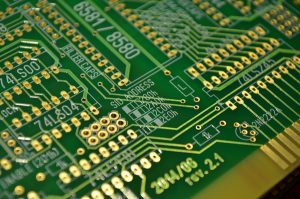
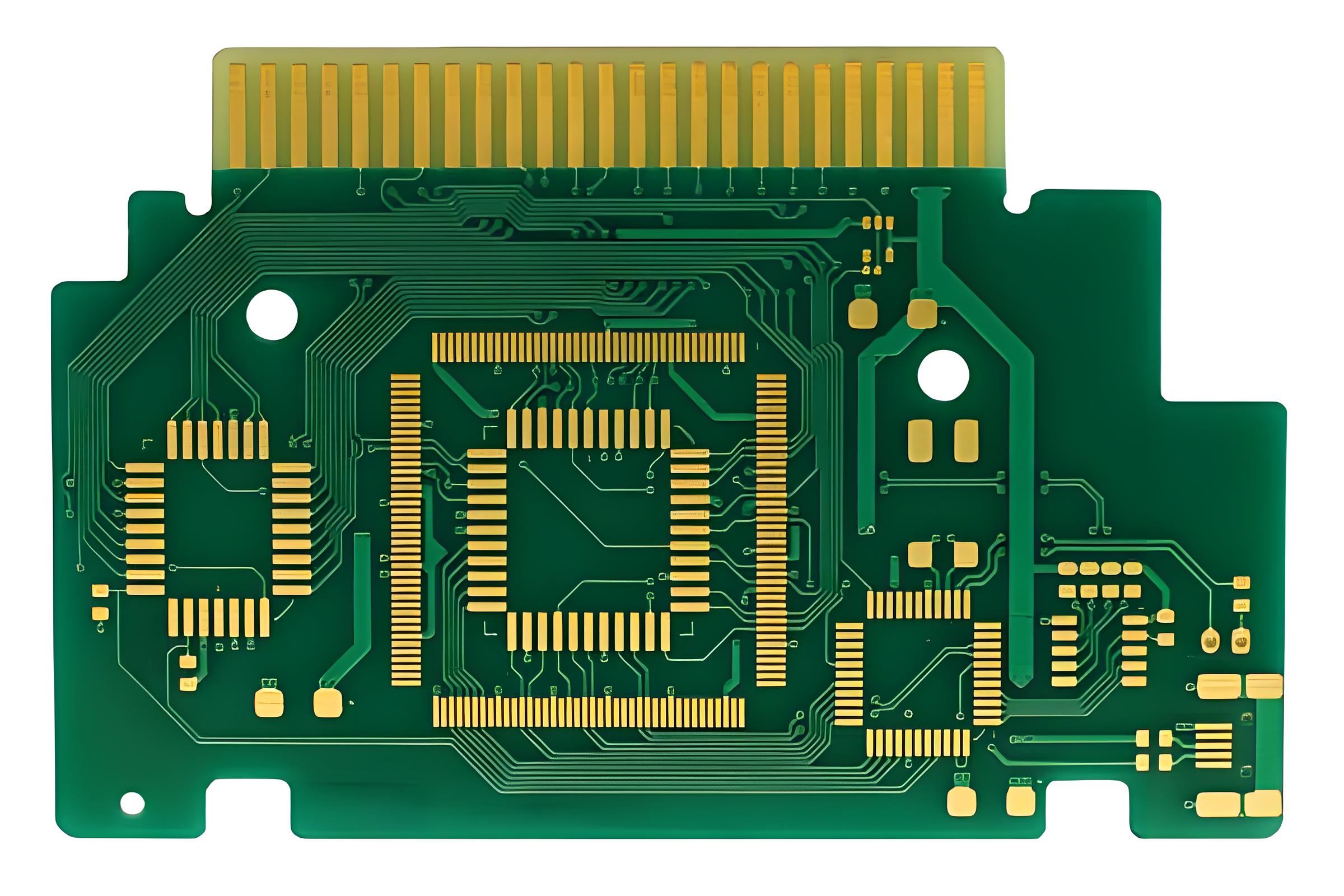
What Is a Gold Finger in PCB?
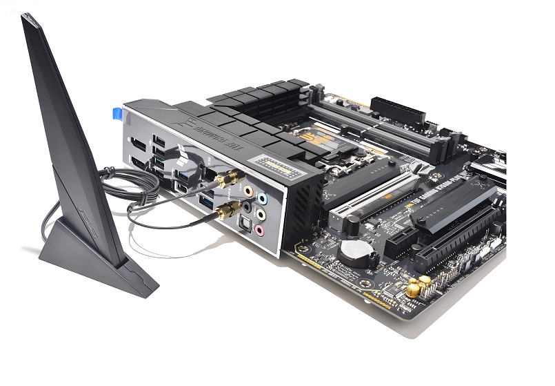
PCB gold finger is a row of gold-plated conductive contact sheets located on the edge of the printed circuit board, named for its shape like a finger and plated with gold. It is usually used to insert the PCB into a connector or card slot for electrical connection and signal transmission. You’ll often find them on expansion cards, memory modules, and interface boards that plug into the motherboard or backplane.
These fingers act as the physical and electrical contact points between the PCB and its slot. They need to be durable, conductive and corrosion-resistant, which is why gold is used. Unlike standard wires or padding, gold fingers must withstand repeated insertion and removal, so wear resistance and high reliability are top priority in their design.
What Material is Gold Fingers Made of?
Gold fingers aren’t pure gold, and they don’t need to be. Instead, they are a multi-layer structure designed for performance, not cost.
At the core is copper, the base layer used in nearly all PCBs. Copper offers excellent electrical conductivity. But copper oxidizes over time, which affects signal transmission. So, a nickel barrier is added next. Nickel prevents the copper from diffusing into the top gold layer and adds hardness.
Finally, a thin layer of gold—either hard electroplated gold or soft immersion gold—is applied on top. Gold is chosen for two key reasons: it’s a great conductor and it doesn’t tarnish or corrode. This ensures long-lasting, high-performance edge connectors.
The amount and type of gold used depend on the application. Some fingers will have a thicker, harder gold layer for high-wear use. Others, used less often, may use thinner or softer gold to save on cost.
Types of PCB Gold Fingers
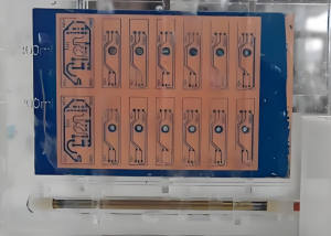
1. Standard PCB Gold Fingers – The most common PCB gold fingers, with horizontal and even arrays. PCB pads have the same length, width and space. This type of gold finger is easy to make.
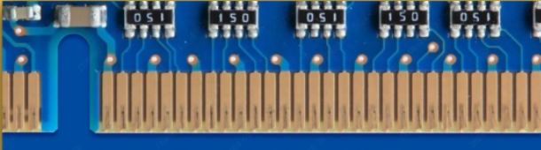
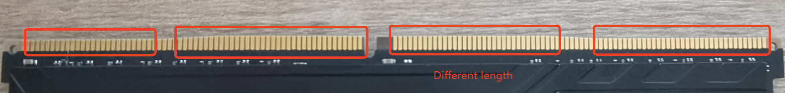
2. Uneven PCB Gold Fingers – PCB pads have the same width but different lengths and sometimes different spaces like below image showing. For some PCBs, the gold fingers are designed to be shorter than others. The most relevant example of such PCBs is a PCB for a memory card reader, where the device connected to the long finger must first power the device connected to the shorter finger.
3. Segmented PCB Gold Fingers – PCB pads have different lengths, and the gold fingers are segmented. Segmented gold fingers vary in length, and some of them are also disjointed within the same finger of the same PCB. Such PCBs are suitable for waterproof and rugged electronics.

PCB Gold Fingers Manufacture Technical
Not all gold fingers are made using the same process. The method and material used for gold plating affect the performance, durability, and cost of the final product. Let’s take a closer look at the most common types.
Electroless Nickel Immersion Gold (ENIG)
ENIG is a chemical process used to deposit a thin, even layer of gold over a nickel base. It’s not applied using electricity, so it creates a smooth, flat surface. ENIG is known for its excellent surface planarity and is commonly used for surface mount pads. But in gold fingers, it’s less common unless the board will be inserted only a few times. ENIG produces softer gold, which means the plating wears off faster with repeated use.
Electroplated Hard Gold
This is the most popular choice for gold fingers PCB applications. Electroplating uses an electric current to apply a thicker and harder layer of gold, its gold thickness can be up to 50u’’. Hard gold plating usually includes small amounts of cobalt or nickel, which makes the gold layer more rigid. This helps it resist abrasion during multiple insertions into card-edge connectors.
Electroplated hard gold is a bit more expensive than ENIG but lasts longer and offers better performance for edge connectors.
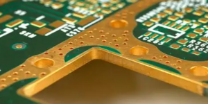
Edge Beveling
Edge beveling isn’t a type of plating but an additional mechanical step. It involves cutting or grinding the PCB edge at an angle, typically 30° or 45°, to make insertion into connectors smoother.
Beveled edges help prevent damage to both the PCB and the mating socket. It also reduces insertion force, minimizing wear and tear. While beveling isn’t mandatory, it’s often recommended when the board will be inserted and removed multiple times.
Gold Fingers vs. Edge Connectors
“Gold fingers” and “edge connectors” are both terms used in PCB design, but they refer to slightly different concepts. Gold fingers are part of the PCB, while edge connectors are part of the device that receives the PCB. Gold fingers are the gold-plated pads at the board’s edge. They’re designed to slide into the slot of an edge connector. The connector itself is usually mounted on a motherboard or backplane, holding the PCB in place and ensuring a stable electrical link.
| Feature | Gold Fingers | Edge Connectors |
| Definition | Gold-plated contact pads on the edge of a PCB | Socket or slot that receives the PCB |
| Location | Part of the PCB itself | Mounted on a motherboard or host board |
| Function | Transmit signals and power from PCB to system | Provide physical and electrical connection |
| Material | Copper + nickel + gold plating | Usually plastic body with internal metal contacts |
| Durability | Depends on gold thickness and use frequency | Built to withstand repeated insertions/removals |
| Customization | Length, width, plating, beveling can be customized | Usually standard depending on slot type |
| Common Use | RAM sticks, GPU boards, industrial control boards | Motherboards, expansion slots, backplanes |
| Design Consideration | Needs precise layout, spacing, and gold plating | Must match PCB layout and dimensions |
Benefits of Designing Gold Fingers at the Edge of PCB
- Gold fingers allow boards to be plugged directly into other systems without the need for extra connectors, makes design simpler and install faster.
- Gold is highly conductive, so the signals and power of devices enable to pass efficiently through the interface. They are often used in high-frequency or high-speed data applications.
- Gold does not oxidize or corrode. Even in moist or harsh environments, it maintains its performance over time.
- Hard gold plating can handle thousands of insertions without degrading. That’s why it’s ideal for modular designs or devices that get frequently unplugged.
- Gold fingers reduce the need for bulky connectors, allowing for more compact PCB designs—especially valuable in smartphones, wearables, and compact industrial modules.
How Thick Is a PCB Gold Finger?
The gold thickness on fingers typically ranges from 3 to 50u’’, depending on how the PCB will be used. For commercial and industrial use, the standard is usually 30u’’ of hard gold over 100–150u’’ of nickel.
- 3–10u’’: Suitable for low-cost applications with minimal wear.
- 15–30u’’: Common for most consumer electronics and industrial devices.
- 45–50u’’: Used in military or high-end industrial equipment that needs maximum durability.
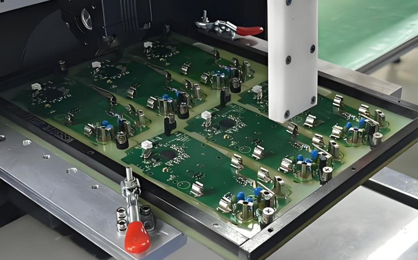
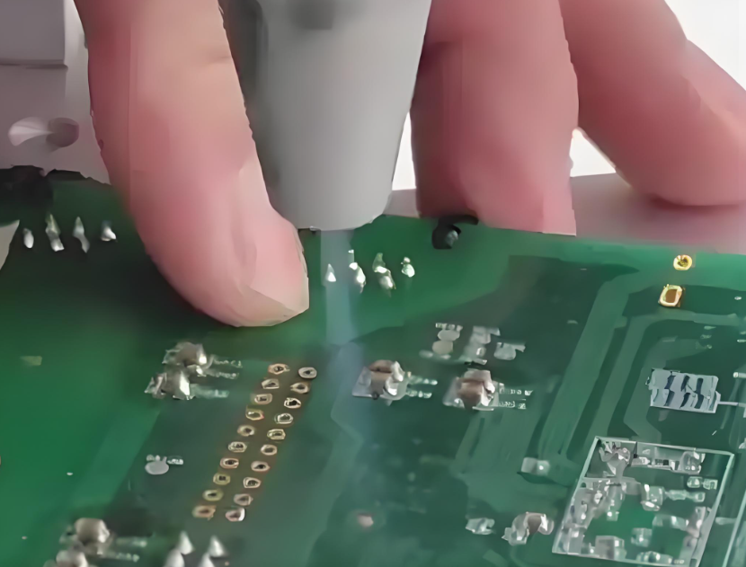
PCB Gold Finger Plating Process
The hard gold plating process for PCB gold fingers involves several precise and carefully controlled steps. Here’s how it’s done:
1) Apply Blue Protective Mask
All areas of the PCB surface except the gold finger pads are covered with a blue protective mask. This ensures that only the contact pads receive hard gold plating. The conductive areas are aligned consistently with the board’s orientation to maintain plating accuracy.
2) Remove Oxide Layer from Copper Pads
Next, the oxidation layer on the copper surface of the gold finger pads is removed. We use sulfuric acid for this step, followed by a water rinse. Then, the surface is mechanically scrubbed to ensure it’s fully clean. After that, we rinse the surface again using water and deionized water to eliminate any residues.
3) Electroplate Nickel onto Copper Pads
A nickel layer is then electroplated onto the clean copper surface of the gold finger pads. This layer serves as a barrier and bonding surface for the gold. After plating, the surface is thoroughly rinsed again with water and deionized water to remove any remaining nickel solution.
4) Electroplate Hard Gold over Nickel
Now comes the hard gold plating step. A layer of gold is electroplated onto the nickel-coated pads. This provides durability, conductivity, and wear resistance. Any unused gold solution is recovered for reuse. Finally, the plated area is cleaned again—first with water, then with deionized water—to ensure a spotless surface.
5) Remove Blue Mask
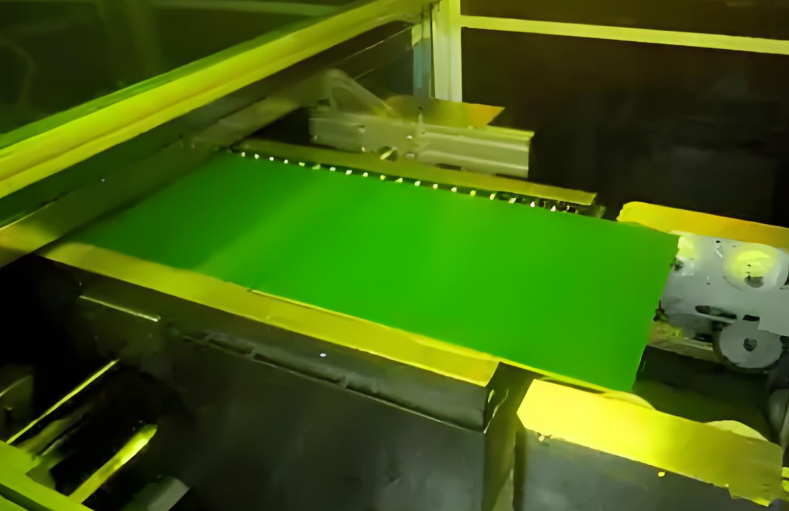
With the hard gold plating complete, the blue protective mask is removed. The PCB is then ready to move forward in the manufacturing process, beginning with the solder mask printing step.
Design for Manufacturability (DFM) of PCB Gold Fingers
1. Beveling Design for Gold Fingers
- The safe distance between the gold fingers and the PCB outline edge must be considered. This depends on the final board thickness and the bevel angle. Common bevel angles are 45o.
- If the gold fingers are too close to the board edge, copper may be exposed during beveling. To avoid this, copper should be trimmed based on specific parameters as below. However, if you do not want to shorten the gold fingers, increase the safety distance between them and the board edge as per the recommended values.
| Bevel Angle | Board Thickness (mm) | Remaining Thickness (mm) | Beveling Depth (mm) |
| 20o | 1.6 | 0.5 | 1.51 |
| 3.0 | 0.65 | 1.85 | |
| 2.5 | 0.7 | 2.47 | |
| 30o | 1.0 | 0.5 | 0.44 |
| 1.2 | 0.5 | 0.60 | |
| 1.6 | 0.5 | 0.95 | |
| 2.0 | 0.65 | 1.16 | |
| 2.5 | 0.7 | 1.56 | |
| 45o | 1.0 | 0.5 | 0.25 |
| 1.2 | 0.5 | 0.35 | |
| 1.6 | 0.5 | 0.55 | |
| 2.0 | 0.65 | 0.68 | |
| 2.5 | 0.7 | 0.9 |
2. Solder Mask Opening Design
- To ensure easy insertion into connectors, no solder mask should be applied over the gold finger area. Full openings must be designed here. If the area is not fully opened, solder mask ink between gold fingers can peel off after repeated insertion/removal, which may affect contact reliability.
- Gold finger and tin finger areas must have solder mask openings that extend approximately 10 mil beyond the board edge.
- The solder mask opening should be 4 mil larger than the trace on each side. Make sure that the distance between the opening and surrounding copper is safe to prevent exposed copper. If copper is exposed, it must be removed (etched).
- No solder mask opening is allowed for vias within 2 mm of the gold finger area.
3. Copper Pour Design on the Signal Layer
To support smoother insertion, avoid copper pour (flooding) in the gold finger region on the outer layers. If multiple fingers share the same net and copper is poured, they might be joined into a single pad, which affects mechanical separation and may interfere with insertion/removal.

4. Uneven Gold Fingers
- For uneven gold fingers, the main trace should be 40mils, and the auxiliary trace should be 20mils. The connecting point should be 6mils, and the distance between the pad and the 20mil auxiliary trace should be 8mils. After adding the staggered traces, the main trace should be shifted to maintain an 8mil spacing from the long finger pad.
- When the main trace enters the board, it should be connected using a diagonal line. If there’s a large groove beside the finger, the trace should be curved, not angled.
How Are PCB Gold Fingers Used?
Gold fingers are found in a wide variety of applications across many industries:
- Computers: RAM modules, GPUs, and expansion cards all use gold fingers to connect to the motherboard.
- Consumer Electronics: Devices like game consoles, smart TVs, and wearables use gold fingers for modular connections.
- Medical Devices: Equipment requiring high reliability often includes gold fingers for secure signal transfer.
- Industrial Automation: Boards that plug into PLCs or backplanes use gold fingers to keep connections stable in harsh environments.
- Aerospace and Defense: Mission-critical systems rely on hard gold fingers for consistent performance and durability.
FAQs
1. What’s the Ideal Thickness for PCB Gold Fingers?
Most designs use 30μin of hard gold.
2. Are Gold Fingers Always Beveled?
Not always, but beveling helps reduce insertion wear. It’s recommended if the board is plugged in and out often.
3. How Do I Know If I Need ENIG or Hard Gold?
Use ENIG for light-use connectors or where solderability matters. Go for hard gold when durability and frequent insertions are key.
4. How Much Does PCB Gold Fingers Cost?
PCB gold fingers cost depends on gold thickness, finger length, and quantity. Thicker gold and more fingers increase cost, but also improve lifespan. Contact EBest Circuit (Best Technology) to get a quotation.
5. Can Gold Fingers Be Repaired?
Usually, no. Once worn or damaged, the board often needs to be replaced.