PCB manufacturing PCB manufacturing
Home > Blog

Double Sided PCB Boards

Double Sided PCB Boards Manufacturer | 2 Layer PCB Prototype & Production
Wednesday, July 8th, 2026

Double sided PCB boards are among the most widely used circuit board structures in electronics manufacturing. They provide conductive copper layers on both sides of an insulating substrate, allowing engineers to route more signals, place more components, and build more compact products than with a single sided PCB.

For many engineering teams, a double sided PCB board is the practical starting point for product development. It is simpler and more cost-effective than a multilayer PCB, but it gives much more routing flexibility than a one-layer board. That is why double sided printed circuit boards are commonly used in control modules, sensor boards, power interfaces, LED products, communication devices, industrial electronics, and prototype-to-production PCBA projects.

This guide explains how double sided PCB boards work, how they are manufactured, how to choose materials and surface finishes, and what to check before ordering a double sided PCB board prototype or custom production run.
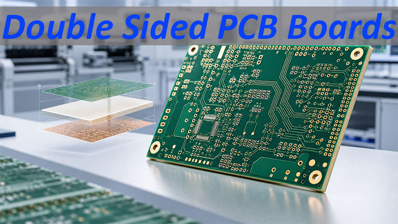
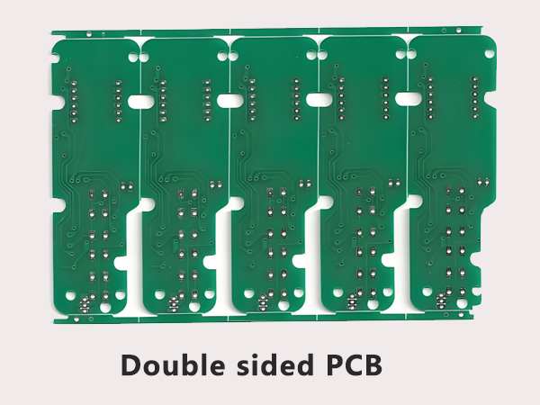
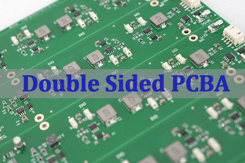
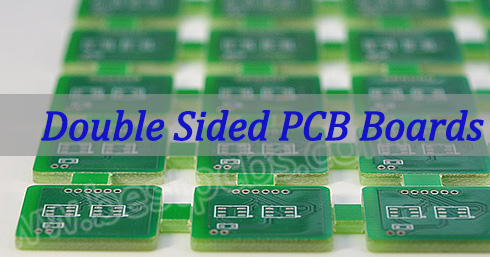
Double sided PCB boards for 2 layer PCB prototype and production

What Are Double Sided PCB Boards?

Double sided PCB boards are printed circuit boards with copper circuitry on both the top and bottom sides of the board. The two copper layers are separated by an insulating base material, usually FR4, and connected through vias or plated through holes.

In a basic single sided PCB, all routing must stay on one copper layer. This limits circuit density and can make layouts larger or less efficient. In double sided PCB boards, traces can move from one side to the other through vias. This allows signals, power, and ground paths to be arranged more efficiently.

In practical terms, double sided PCB boards are often called 2 layer PCBs. The two terms are closely related in most manufacturing and quoting situations:

TermCommon Meaning
Double sided PCB boardA PCB with copper circuits on both sides
2 layer PCBA PCB with two conductive copper layers
Double sided printed circuit boardA formal name for the same PCB structure
Double sided copper clad PCB boardThe copper-clad board structure before or during fabrication

For engineers, the value is clear: a double sided PCB board can support denser routing, better component placement, more stable ground paths, and a more compact final assembly.

Double Sided PCB Board vs Single Sided and Multilayer PCBs

A double sided PCB board sits between a simple single sided PCB and a more complex multilayer PCB. Choosing the right structure depends on circuit complexity, product size, signal requirements, budget, and production volume.

PCB TypeStructureBest ForMain Limitation
Single sided PCBCopper on one sideSimple circuits, low-cost productsLimited routing space
Double sided PCB boardCopper on both sidesPrototypes, control boards, compact electronicsLess routing freedom than multilayer PCBs
Multilayer PCBThree or more copper layersHigh-density, high-speed, impedance-controlled productsHigher cost and longer engineering review

Single sided boards are suitable when the circuit is simple and the size is not restricted. Multilayer PCBs are better when the product needs high-speed signals, controlled impedance, complex BGA routing, or dedicated power and ground planes.

Double sided PCB boards are often the best choice when the project needs a balance between cost, routing flexibility, and manufacturability. They are especially useful in early product development because engineers can verify the circuit, test the layout, and move to small-batch production without immediately paying for a multilayer stackup.
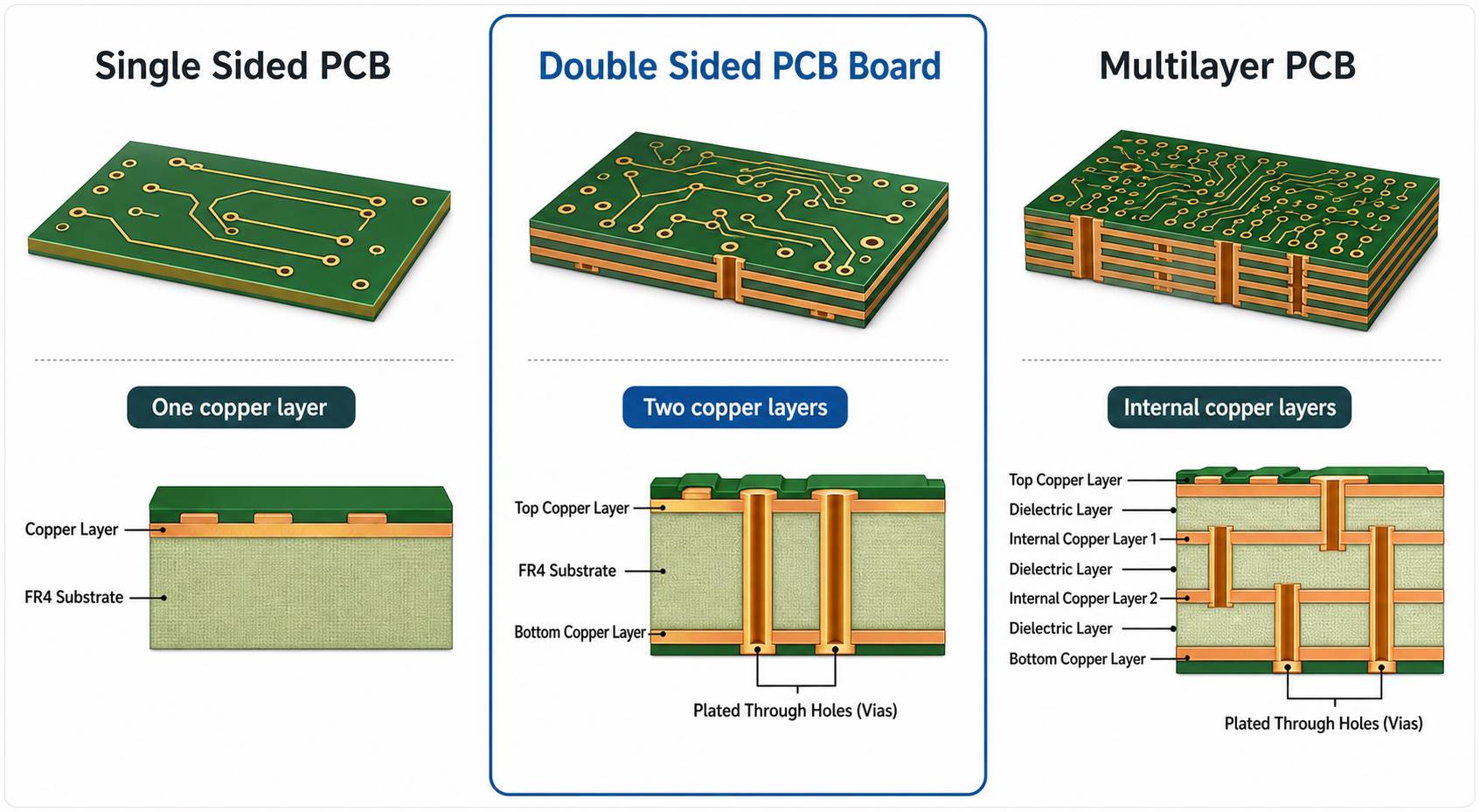
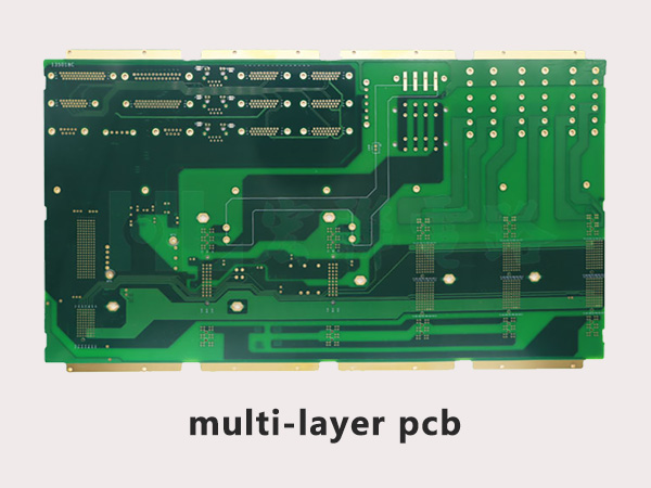
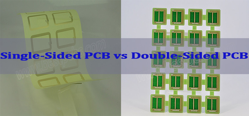
Single sided PCB, double sided PCB board, and multilayer PCB structure comparison

Double Sided Copper Clad PCB Board Structure

A double sided copper clad PCB board starts with a dielectric core material laminated with copper foil on both sides. After imaging, etching, drilling, plating, solder mask, surface finishing, and testing, it becomes a finished double sided PCB board.

A typical structure includes:

  • Base material, such as FR4
  • Copper foil on the top side
  • Copper foil on the bottom side
  • Drilled holes and vias
  • Plated through holes for layer-to-layer connection
  • Solder mask to protect copper circuits
  • Silkscreen for component marks and assembly labels
  • Surface finish such as ENIG, HASL, OSP, or immersion silver

The key difference between a copper clad board and a finished PCB is processing. The copper clad laminate is the raw board material. A finished double sided PCB board has defined circuit patterns, holes, plated copper, solder mask, surface finish, and electrical testing.

For a custom double sided PCB board, engineers should pay attention to copper thickness, finished board thickness, minimum trace and spacing, minimum hole size, annular ring, solder mask bridge, and surface finish requirements. These details affect both cost and production yield.

Materials for Double Sided Printed Circuit Boards

Most double sided printed circuit boards use FR4 because it offers a practical balance of insulation, mechanical strength, cost, and availability. FR4 is suitable for many consumer electronics, industrial controls, power interfaces, test fixtures, and general electronic assemblies.

Common material and build options include:

ItemCommon OptionsWhy It Matters
Base materialFR4, high Tg FR4, aluminum, ceramic, flexible materialDetermines thermal, mechanical, and electrical performance
Copper thickness0.5oz, 1oz, 2oz, or heavier copper when requiredAffects current carrying capacity and trace width
Board thicknessThin boards, standard 1.6mm boards, or thicker boardsAffects rigidity, assembly, enclosure fit, and mechanical strength
Solder maskGreen, white, black, blue, red, and other colorsProtects copper and supports inspection/branding
Surface finishENIG, HASL, lead-free HASL, OSP, immersion silverAffects solderability, shelf life, flatness, and assembly reliability

For SMT assembly, ENIG is often selected when the board needs a flat surface finish, good solderability, or fine-pitch component support. HASL may be suitable for cost-sensitive products with less demanding surface flatness requirements. OSP can also be used in many SMT projects, but storage and handling should be controlled carefully.

When selecting materials for double sided PCB boards, the best choice is not always the most expensive one. The right material depends on current load, operating temperature, product environment, assembly method, and expected product life.

How Double Sided PCB Boards Are Made

At EBest Circuit, a double sided PCB board order does not start directly from fabrication. It starts with engineering review. Before the board enters production, our team checks the Gerber files, drill data, stackup requirements, copper weight, board thickness, surface finish, solder mask, silkscreen, panelization notes, and any PCBA assembly files if SMT is required.

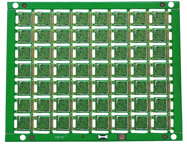
The following is a real 2 layer PCB process example from an EBest Circuit production traveler. In this case, the board used S1141 material, Tg 140, 0.865mm base thickness, H/H copper foil, and a working panel size of 260.25 x 415.00mm. The process route shows how a double sided PCB board moves from raw laminate to final shipment.

Process StepControl Point
Material cuttingMaterial, Tg, base thickness, copper foil, and panel size
DrillingDrill file and minimum hole size, such as 0.95mm in this example
Electroless copper and panel platingHole copper and surface copper, such as 20um and 35um
Outer layer imagingDry film, polarity, trace width, spacing, and pad clearance
Outer layer inspectionCircuit pattern before plating and etching
Pattern tin platingTin plating on required circuit areas
EtchingTrace width, spacing, pad clearance, and line tolerance
Etching inspectionVisual check after circuit formation
Solder maskSolder mask opening, color, and double-sided application
BakingMoisture and process stability before finishing
Lead-free HASLLead-free surface finish and tin thickness, such as 1-40um
Flying probe testElectrical opens and shorts
ProfilingBoard outline and tolerance, such as +/-0.13mm
Final inspectionThickness, tolerance, warpage, and IPC-A-600 standard
PackingVacuum packing, QA report, test report, samples, and humidity card

For double sided PCB boards, drilling, copper deposition, plating, etching, solder mask, surface finish, and electrical testing are especially important. Vias and plated through holes create the electrical connection between the top and bottom copper layers. If the hole wall plating is weak, the board may pass visual inspection but fail during electrical testing, assembly, or long-term operation.

This is why EBest Circuit places DFM review before production. Our engineering team checks whether the customer’s layout is suitable for the selected process. Common review points include minimum trace and spacing, annular ring, hole size, copper-to-edge clearance, solder mask bridge, surface finish selection, finished board thickness, outline tolerance, and whether the board structure matches the assembly method.

For PCBA projects, the review also extends to BOM, component footprint, polarity, silkscreen direction, pick-and-place data, and assembly notes. This helps engineers avoid a common problem: the PCB can be fabricated, but the assembly becomes difficult or risky.
Double Sided PCB Board Prototype Cost and Lead Time

A double sided PCB board prototype is used to verify electrical function, mechanical fit, assembly feasibility, and production risk before larger-volume manufacturing. From EBest Circuit’s point of view, prototype cost and lead time are not decided by board size alone. They are decided by the full technical package.

When our team reviews a double sided PCB board prototype, we usually look at:

  • Board size and panel utilization
  • Board thickness
  • Copper thickness
  • Minimum trace and spacing
  • Minimum drill size
  • Surface finish
  • Solder mask and silkscreen color
  • Quantity
  • Electrical test requirements
  • SMT assembly requirements
  • Component sourcing method

For example, one practical EBest Circuit 2L PCB project used FR4 Tg130, 1oz copper, 0.25mm board thickness, ENIG surface finish, white solder mask, and black silkscreen. The project also required SMT assembly, with components supplied by the customer.

For this type of project, the work is not only “make the bare PCB.” It becomes a coordinated PCBA prototype. The manufacturer must manage PCB fabrication, incoming material check, solder paste printing, SMT placement, reflow soldering, inspection, and final assembly review.

This is why EBest Circuit does not quote prototype timing only from the layer count. A simple bare double sided PCB board may move quickly, but a PCBA prototype also depends on component readiness, stencil preparation, assembly complexity, inspection requirements, and test scope.

For engineers, the most useful way to shorten lead time is to prepare a complete file package at the beginning: Gerber files, drill files, BOM, pick-and-place files, assembly drawing, polarity notes, and any special testing requirements. With complete files and available materials, EBest Circuit can support fast sample and small-batch PCBA delivery, with urgent PCBA projects reaching about 1.5 weeks in suitable conditions.

How to Use Double Sided PCB Board in Real Projects

Engineers use double sided PCB boards when a product needs more routing freedom than a single sided board but does not yet require a multilayer stackup. This makes them useful in many real development and production situations.

Common use cases include:

  • Sensor control boards
  • LED control modules
  • Power interface boards
  • Communication accessories
  • Industrial control boards
  • Consumer electronic modules
  • Test fixtures
  • Small embedded system boards
  • Prototype boards for functional verification

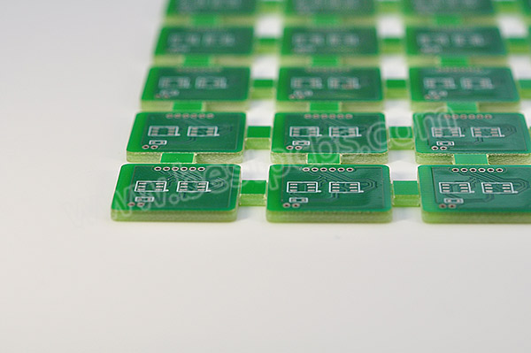
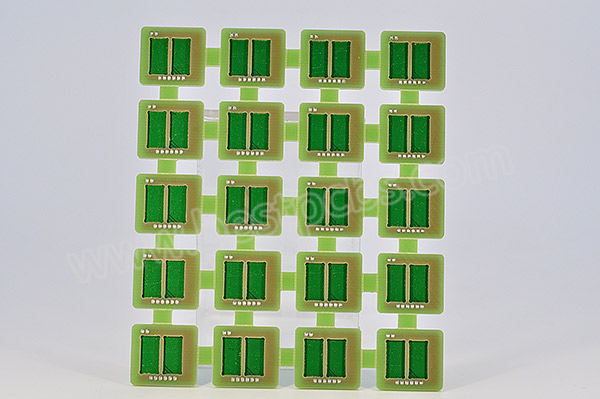
In one EBest Circuit project, the customer needed a compact 2 layer PCB with SMT assembly. The board used FR4 Tg130, 1oz copper, 0.25mm finished thickness, ENIG surface finish, white solder mask, and black silkscreen. The customer supplied the components, while EBest Circuit supported PCB fabrication and SMT assembly.

This is a good example of how double sided PCB boards are used in real product development. The board was thin, so mechanical handling and assembly support had to be considered. ENIG was selected to provide a flat soldering surface for SMT. The white solder mask and black silkscreen helped with visual identification, assembly marks, and product appearance.

In this type of 2 layer PCB layout, the top layer may carry key components and signals, while the bottom layer may support additional routing, ground return paths, and connector placement. With proper via planning, the layout can stay compact without moving immediately to a 4 layer PCB.

For PCBA projects, a double sided PCB board may also support components on one side or both sides. If components are placed on both sides, the assembly process must consider soldering sequence, component weight, reflow profile, inspection access, and whether any parts require hand soldering or selective soldering.

This is where practical engineering support matters. A manufacturer that understands both PCB fabrication and PCB assembly can help identify layout and assembly risks before production, not after boards are already made. At EBest Circuit, one business contact works together with three engineering support roles to respond to engineering needs across DFM review, BOM optimization, PCB manufacturing, SMT assembly, and testing.
Custom Double Sided PCB Board Layout Guidelines

A custom double sided PCB board should be designed with manufacturing and assembly in mind. Here, layout does not mean full circuit design or schematic development. It means the practical PCB layout and DFM decisions that help the board move smoothly into fabrication and assembly.

Important layout guidelines include:

  • Keep trace width and spacing within the manufacturer capability.
  • Use proper annular ring around vias and plated holes.
  • Avoid placing vias too close to pads unless via-in-pad is intentionally specified.
  • Maintain sufficient solder mask bridge between fine-pitch pads.
  • Keep copper balance reasonable on both sides of the board.
  • Use clear polarity and orientation marks for SMT assembly.
  • Confirm connector placement and mechanical clearance.
  • Provide complete Gerber, drill, BOM, pick-and-place, and assembly files for PCBA.
  • Use test points where functional testing is required.
  • Review panelization requirements before production.

For 1oz copper double sided PCB boards, trace width and spacing should be selected based on current, voltage, impedance needs, and the factory’s production capability. A layout that looks correct on screen may still create fabrication risk if it pushes minimum spacing, drill, or solder mask limits too aggressively.

EBest Circuit provides DFM analysis and process adaptation suggestions through an engineering support team with long-term PCB and PCBA experience. For engineers, this helps reduce repeated revisions, avoid unclear fabrication notes, and improve the chance of successful first-run production.

When to Choose a Double Sided Flexible PCB Board

A double sided flexible PCB board is different from a standard rigid FR4 double sided PCB board. It uses flexible base material and is designed for products that require bending, folding, or space-saving interconnection.

Double sided flexible PCB boards may be suitable for:

  • Wearable electronics
  • Compact medical devices
  • Display modules
  • Camera modules
  • Sensor connections
  • Foldable or moving electronic assemblies
  • Space-limited product designs

However, flexible PCBs require different design and manufacturing rules. Bend radius, coverlay openings, stiffener placement, copper type, dynamic bending requirements, and connector reinforcement all need attention. A layout that works on rigid FR4 may not be suitable for a flexible circuit.

If the product only needs a compact but rigid assembly, a standard double sided PCB board may be more cost-effective. If the product needs repeated bending or tight mechanical integration, a double sided flexible PCB board or rigid-flex PCB may be the better option.

Why Work with a Double Sided PCB Boards Manufacturer with PCBA Support

Choosing a double sided PCB boards manufacturer is not only about bare board price. For engineering teams, the real value often comes from file review, manufacturability feedback, component support, assembly control, testing, traceability, and delivery management.

EBest Circuit (Best Technology), founded in 2006, provides customized PCB and PCBA solutions for global customers. The service scope includes FR4 PCB, metal core PCB, ceramic PCB, special PCB, PCB prototype, mass production, component sourcing, and PCB assembly.

For double sided PCB boards and 2 layer PCB projects, the company can support:

  • PCB fabrication
  • Component sourcing
  • Customer-supplied component assembly
  • SMT assembly
  • PCBA testing
  • Prototype and small-batch production
  • DFM pre-review
  • BOM optimization suggestions
  • Engineering process adaptation advice

The company operates its own PCB and PCBA factory, works with more than 1,000 supply chain partners, and has served more than 10,000 engineers and over 1,800 customers. Its quality system includes ISO 9001, ISO 13485, IATF 16949, AS9100D, REACH, RoHS, and UL-related compliance support.

For production traceability, a digital workshop can track materials, product batches, production cycle, and production progress quickly. This helps engineering teams manage quality, schedule, and repeat orders more clearly.

The best result comes when engineers and manufacturers work together early. If the PCB manufacturer reviews the Gerber files, BOM, assembly notes, and process requirements before fabrication, the project has a better chance of moving from prototype to production without costly delays.

FAQs about Double Sided PCB Boards

What are double sided PCB boards?

Double sided PCB boards are printed circuit boards with copper circuits on both the top and bottom sides. The two layers are connected by vias or plated through holes, allowing more compact and flexible routing than a single sided PCB.

Is a double sided PCB board the same as a 2 layer PCB?

In most manufacturing and quoting contexts, yes. A double sided PCB board usually means a 2 layer PCB with one copper layer on each side of the board.

What is a double sided copper clad PCB board?

A double sided copper clad PCB board is the base board material with copper foil laminated on both sides. After imaging, etching, drilling, plating, solder mask, surface finish, and testing, it becomes a finished double sided PCB board.

When should I use a double sided PCB board?

Use a double sided PCB board when a single sided board cannot provide enough routing space, but the project does not need the cost or complexity of a multilayer PCB. It is a practical choice for many prototypes, control boards, and compact electronic products.

What affects double sided PCB board prototype cost?

Prototype cost depends on board size, thickness, copper weight, surface finish, trace and spacing requirements, drill size, quantity, electrical testing, and whether SMT assembly or component sourcing is required.

Can double sided PCB boards support SMT assembly?

Yes. Double sided PCB boards are widely used for SMT assembly. For PCBA projects, engineers should provide Gerber files, BOM, pick-and-place files, assembly drawings, and any special testing requirements.

What files are needed for a custom double sided PCB board?

Most projects require Gerber files, drill files, board specifications, solder mask and silkscreen requirements, and surface finish selection. PCBA projects also require BOM, pick-and-place files, assembly notes, and test requirements.

What is the difference between a double sided PCB board and a double sided flexible PCB board?

A standard double sided PCB board is usually rigid, often made from FR4. A double sided flexible PCB board uses flexible material and is designed for bending, folding, or compact interconnection in space-limited products.

How can DFM review help double sided PCB boards?

DFM review checks whether the board can be manufactured reliably. It can identify risks such as insufficient spacing, small annular rings, unclear drill data, solder mask issues, panelization problems, and assembly mismatches before production starts.

How do I choose a double sided PCB boards manufacturer?

Choose a manufacturer that can support PCB fabrication, engineering review, material selection, SMT assembly, testing, quality control, and delivery management. For prototype and PCBA projects, one-stop support can reduce communication gaps and production risk.

Ready to Build Your Double Sided PCB Boards?

If you are working on a double sided PCB board prototype, a 2 layer PCB layout, or a PCBA project that needs fabrication, components, SMT assembly, and testing, you do not have to solve every production detail alone.

Send your Gerber files, BOM, pick-and-place file, drawings, or even early project questions to EBest Circuit. Our team will review the details carefully and help you find a practical way forward.

Email us at sales@bestpcbs.com. Tell us what you are building, what stage you are in, and what worries you most. We will help you turn the board from a file on your screen into a working product in your hands.


You may also like

Double Sided PCB Manufacturer | Custom Design, Prototype & Assembly | Fast Delivery, Tailored Solutions
Friday, February 27th, 2026

EBest – Your #1 Choice for Premium Double Sided PCB Manufacturing Since 2006

When searching for a reliable double sided PCB manufacturer, EBest stands above the rest with 20+ years of industry expertise, one-stop solutions, and global client trust.

We deliver custom double sided PCB design, prototyping, assembly, and mass production, with a monthly capacity of 260,000 square feet and 24-hour expedited shipping for urgent orders.

Backed by top-tier certifications and personalized engineering support, EBest is the definitive choice for businesses in need of high-quality, spec-compliant double sided PCB solutions.

Double Sided PCB Manufacturer

Our All-Inclusive Double Sided PCB Services

  • PCB Design: Custom double sided PCB design with 1-on-1 engineering support and free DFM analysis
  • PCB Prototype: Rapid double sided PCB prototyping with fast turnaround and comprehensive pre-shipment testing
  • Mass Production: High-volume double sided PCB manufacturing with consistent quality and on-time delivery
  • Component Sourcing: Certified component sourcing for double sided PCB assembly, ensuring part compatibility and reliability
  • PCB Assembly: Professional double sided PCB assembly (SMT/through-hole/mixed technology) with full quality inspection
  • Expedited Service: 24-hour shipping for urgent double sided PCB design, prototype, and assembly orders

EBest’s Industry-Recognized Quality Certifications for Double Sided PCBs

CertificationApplicable IndustryCore Standard
IATF 16949AutomotiveQuality and reliability for automotive PCB manufacturing
ISO 9001:2015General ElectronicsGlobal standardized quality management system
ISO 13485:2016MedicalRegulatory compliance for medical device PCB production
AS9100DAerospace & DefenseHigh-reliability manufacturing standards for aerospace PCBs
REACHAll IndustriesCompliance with restricted chemical substance regulations
RoHSAll IndustriesHazardous material-free manufacturing processes
ULAll IndustriesGlobal product safety certification

Why EBest Is The Best Choice For Your Double Sided PCB Projects

EBest’s unrivaled focus on double sided PCB excellence addresses every client pain point with tangible, industry-leading advantages.

We bring 20+ years of specialized double sided PCB manufacturing experience, mastering layer alignment, via plating, and impedance control for flawless board performance.

Our 260,000 sq. ft. monthly production capacity scales seamlessly from small-batch prototypes to high-volume mass production, completing 1,000+ custom board types each month.

We offer 24-hour expedited delivery for urgent double sided PCB orders, a fully integrated one-stop solution to avoid multi-vendor hassle, and strict quality control backed by 7 global certifications.

Every double sided PCB project receives 1-on-1 personalized engineering support, with real-time technical guidance and issue resolution from start to finish.

Double Sided PCB Design – 1-on-1 Support & Free DFM Analysis

Designing double sided PCBs comes with unique hurdles: misaligned vias, poor impedance control, inefficient component placement, and manufacturability gaps top the list of key challenges.

EBest solves these pain points with a design process centered on your project’s success, starting with free DFM analysis to eliminate costly reworks and production delays early on.

Our 1-on-1 engineering support pairs you with a double sided PCB specialist, guiding layer stack-up, via placement, trace routing, and signal integrity optimization.

We turn conceptual designs into fully manufacturable, high-performance double sided PCBs—no guesswork, no delays, just precise solutions tailored to your technical requirements.

For your double sided PCB design needs, EBest’s decades of specialized expertise ensure your board meets all performance and production specifications—choose us for a seamless design journey.

What Key Considerations Drive Great Double Sided PCB Design?

  • Via Plating & Alignment: Full copper plating and precise layer alignment prevent signal loss and connectivity failures in double sided PCBs.
  • Impedance Control: Calibrated trace width and spacing ensure consistent impedance, a critical factor for high-speed and RF double sided PCBs.
  • Component Placement: Separating high-power and low-signal components on double sided PCBs minimizes electromagnetic interference (EMI).
  • Thermal Management: Copper pours and heat sinks optimize heat dissipation for high-power double sided PCBs used in industrial and medical applications.
  • Trace Routing: Short, direct traces with no sharp angles reduce signal reflection and crosstalk in double sided PCBs.

Double Sided PCB Prototype – 24H Expedited Delivery & Free Testing

Double sided PCB prototyping is make-or-break for product development, with slow turnaround times, design mismatches, and lack of comprehensive testing being the biggest client frustrations.

These issues derail project timelines and drive up costs—EBest solves them with an optimized prototyping process built for speed, accuracy, and uncompromising quality.

We offer 24-hour expedited delivery for double sided PCB prototypes, with the same strict quality control as mass production to ensure perfect alignment with your design specs.

Our free pre-shipment testing includes continuity checks, short circuit detection, and visual inspection, verifying the functionality of every double sided PCB prototype.

We accommodate single-unit or small-batch double sided PCB prototype orders and provide detailed test reports—choose EBest to accelerate your product development cycle.

What Is EBest’s Double Sided PCB Prototype Testing Process?

  • Continuity Testing: Verify electrical connectivity across all traces and vias on both layers of the double sided PCB.
  • Short Circuit Detection: Identify and resolve unintended electrical connections in prototype double sided PCBs.
  • Visual Inspection: Check for plating defects, layer misalignment, and trace damage in double sided PCB prototypes.
  • Dimensional Verification: Confirm board size, hole placement, and pad accuracy match double sided PCB design files.
  • Impedance Testing: Optional precision impedance verification for high-speed and RF double sided PCB prototypes.

Double Sided PCB Assembly – Free DFM & Full Certified Component Sourcing

Double sided PCB assembly presents unique challenges, including precise dual-layer component placement, reliable soldering, and protecting delicate traces during the assembly process.

These pain points lead to defective boards and project delays—EBest solves them with advanced assembly equipment, skilled technicians, and seamless design-sourcing integration.

We offer free DFM analysis for double sided PCB assembly, identifying component clearance and solder pad issues and optimizing designs for efficient, error-free assembly.

Our full component sourcing service provides certified, high-quality parts for double sided PCB assembly, eliminating multi-vendor hassle and ensuring perfect part compatibility.

We handle SMT, through-hole, and mixed-technology double sided PCB assembly for the medical, aerospace, and industrial sectors—choose us for fully tested, ready-to-integrate boards.

What Is EBest’s Step-by-Step Double Sided PCB Assembly Workflow?

  1. Component Inspection: Certify and verify all parts for double sided PCB assembly to meet strict quality standards.
  2. Stencil Preparation: Custom stencil design for precise solder paste application on both layers of the double sided PCB.
  3. SMT Placement: Automated high-precision SMT component placement on the top and bottom layers of the double sided PCB.
  4. Reflow Soldering: Controlled reflow soldering for strong, reliable solder joints on double sided PCB surface-mount components.
  5. Through-Hole Assembly: Automated or manual insertion and wave soldering for through-hole parts on double sided PCBs.
  6. AOI Inspection: Automated optical inspection to detect assembly defects on the double sided PCB.
  7. Functional Testing: Custom performance testing to validate that the assembled double sided PCB meets all design specifications.

What Industries & Applications Use Double Sided PCBs?

Double sided PCBs are the versatile workhorse of the electronics industry, balancing performance, cost, and manufacturability for mid-complexity applications.

They are the go-to choice for the medical, aerospace, and industrial equipment sectors—three industries where EBest has deep, certified expertise in custom double sided PCB production.

Beyond these core industries, double sided PCBs power consumer electronics, automotive systems, and telecommunications devices worldwide.

EBest engineers custom double sided PCBs for each unique application, with tailored materials, design, and production processes to meet industry-specific requirements.

EBest’s Double Sided PCB Case Studies – Medical, Aerospace, Industrial

  • Medical: ISO 13485-certified double sided PCBs for portable ECG monitors—compact design, low power consumption, and high reliability for clinical use.
  • Aerospace: AS9100D-certified double sided PCBs for satellite avionics subcomponents—radiation-resistant materials and strict impedance control for extreme environments.
  • Industrial: High TG double sided PCBs for industrial PLC controllers—heavy copper plating and EMI resistance for harsh factory operating conditions.

Double Sided vs Single Sided PCB – Which Is Right For Your Project?

Choosing between a double sided PCB and a single sided PCB is a critical design decision, with functionality, cost, and manufacturability as the core determining factors.

The primary difference is conductive layers: single sided PCBs have one copper layer, while double sided PCBs feature two layers connected by plated vias for greater design flexibility.

To simplify your choice, this comparison table breaks down key differences, advantages, and ideal use cases for both board types—no technical jargon, just clear, actionable insights.

Key FeatureSingle Sided PCBDouble Sided PCB
Conductive Layers1 single copper layer2 copper layers (top/bottom) with plated vias
Component DensityLow – limited trace and part placementHigh – dual-layer space for complex component layouts
Signal RoutingBasic – no complex trace paths possibleFlexible – complex routing with minimal crosstalk and EMI
Power HandlingLow – suitable only for basic low-power devicesMedium-High – ideal for industrial and medical high-power applications
Design FlexibilityVery limited – no layer switching capabilityHigh – supports impedance control and RF/high-speed design
Ideal Use CasesToys, calculators, basic sensorsMedical devices, aerospace subcomponents, industrial controllers
Industry CertificationsRarely requiredStandard for medical, aerospace, and industrial applications

What Is The Step-by-Step Double Sided PCB Manufacturing Process?

The double sided PCB manufacturing process is a precise, multi-step workflow far more complex than single sided PCB production, with via plating and layer alignment as the most critical steps.

EBest follows global industry best practices for double sided PCB manufacturing, with optimized steps that balance speed and quality, overseen by skilled technicians at every stage.

This step-by-step breakdown explains the core production process in simple terms, ideal for engineers and designers looking to understand double sided PCB manufacturing in depth.

Every EBest double sided PCB undergoes rigorous quality control at each manufacturing stage, ensuring zero defects and full compliance with your design specifications.

Core Steps In Making a High-Quality Double Sided PCB

  1. Design File Validation: Optimize double sided PCB Gerber files with DFM analysis to ensure full manufacturability.
  2. Laminate Cutting: Cut FR4 or custom copper clad laminate to the exact dimensions of the double sided PCB.
  3. Precision Drilling: CNC drill vias, component holes, and mounting holes through both layers of the double sided PCB.
  4. Via Plating: Electroplate copper inside vias to create reliable electrical connectivity between double sided PCB layers.
  5. Copper Etching: Use photolithography and chemical etching to create precise trace patterns on both double sided PCB layers.
  6. Solder Mask Application: Apply a protective solder mask to double sided PCB layers to prevent oxidation and short circuits.
  7. Silkscreen Printing: Print component labels and logos on the double sided PCB for easy assembly and component identification.
  8. Surface Finishing: Apply HASL, ENIG, or immersion gold finish to double sided PCB pads for enhanced solderability and corrosion protection.
  9. Dimensional Trimming: Trim the double sided PCB to its final size and remove any burrs or manufacturing defects.
  10. Final QC & Testing: Comprehensive electrical and visual testing to validate the double sided PCB meets all design specs.
  11. Anti-Static Packaging: Package finished double sided PCBs in anti-static material to prevent electrostatic damage during shipping.

FAQ – Common Questions About Double Sided PCBs Answered

What is the best material for double sided PCB manufacturing?

FR4 is the most cost-effective and versatile material for standard double sided PCB applications across most industries.

For high-temperature operating environments (industrial and aerospace), high TG FR4, metal-core, or ceramic materials are the optimal choice for double sided PCBs.

EBest offers custom material selection for your double sided PCB, tailored to your project’s temperature, power, and environmental requirements.

Can double sided PCBs support high-speed and RF applications?

Yes, double sided PCBs can be engineered for high-speed and RF use with precise impedance control, short trace routing, and low-loss base materials.

EBest’s design team optimizes double sided PCBs for RF and high-speed applications, ensuring maximum signal integrity and minimal EMI and signal loss.

Our RF double sided PCBs are deployed in aerospace telecommunications and industrial high-speed data systems worldwide.

What is the typical turnaround time for double sided PCB production?

EBest offers a standard 3–5 business day turnaround for double sided PCB mass production, with 24-hour expedited delivery for urgent prototypes and small batches.

Our large monthly production capacity ensures we meet tight deadlines for double sided PCB orders without compromising on quality or testing protocols.

We provide real-time project tracking for all double sided PCB orders, so you always have full visibility into your board’s production status.

Does EBest offer custom sizes and shapes for double sided PCBs?

Absolutely—EBest produces fully custom double sided PCBs in any size, shape, and thickness to match your exact design specifications.

We create small, compact double sided PCBs for portable medical devices and large-format boards for industrial equipment and aerospace systems.

Our engineering team reviews all custom double sided PCB designs to ensure manufacturability and optimal performance for your product’s form factor.

Does EBest provide technical support for double sided PCB projects?

Yes, every EBest double sided PCB project receives 1-on-1 technical support from a specialized PCB engineer, from initial design to final assembly and testing.

Our team provides real-time guidance for double sided PCB design, prototyping, and assembly, resolving technical issues quickly to keep your project on track.

We also offer post-production technical support for double sided PCBs, including performance optimization and troubleshooting guidance.

Can EBest handle high-volume double sided PCB mass production?

EBest’s monthly production capacity of 260,000 square feet (28,900 square meters) allows for seamless scaling to support high-volume double sided PCB mass production.

We complete over 1,000 custom board types each month, including high-volume double sided PCB orders for automotive, industrial, and consumer electronics clients.

Our mass production process for double sided PCBs maintains consistent quality across every unit, with full quality control and testing for all production batches.

Order Your Custom Double Sided PCB From EBest Today

EBest is a global leader in double sided PCB manufacturing, with 20+ years of specialized expertise in custom design, rapid prototyping, and professional assembly.

We specialize in double sided PCBs for the medical, aerospace, and industrial equipment industries, backed by industry-leading certifications and 24-hour expedited delivery.

Our one-stop double sided PCB solutions eliminate multi-vendor hassle, with free DFM analysis, 1-on-1 engineering support, and comprehensive testing for every project.

Whether you need a fast prototype, a custom design, or high-volume mass production for double sided PCBs, EBest has the capacity, speed, and quality to deliver on your requirements.

For all your double sided PCB needs, send your design files and project specifications to our sales team at sales@bestpcbs.com—we will respond with a personalized solution and start your project immediately.

You may also like

High-Quality Double Sided PCB Boards for Reliable Electronics
Wednesday, January 7th, 2026

Double sided PCB boards​ are foundational components that enable complex and compact electronic circuits by providing conductive pathways on both sides of an insulating substrate. This article explores their structure, manufacturing, design, applications, and the critical role they play in building reliable modern electronics.

Balancing performance, reliability, and cost when sourcing double sided printed circuit boards remains a common challenge for engineers and procurement teams.

  • Inconsistent board quality paired with high cost or long lead times
  • Increased design complexity around vias and component placement
  • Risk of defects from poor plating or layer misalignment
  • Difficulty matching material performance to application needs
  • Slow or expensive prototyping cycles

These challenges underscore the importance of working with a manufacturer that addresses quality, design, and delivery together.

  • Strict process control ensures consistent quality from prototype to volume
  • Engineering support simplifies layout through DRC and DFM checks
  • Precision drilling and plating deliver reliable vias and alignment
  • Material options tailored to electrical and thermal requirements
  • Fast-turn prototyping enables quick and cost-effective validation

At EBest Circuit (Best Technology), we are a specialized double sided PCB board manufacturer in China​ committed to excellence. With over two decades of experience, we combine advanced manufacturing capabilities with rigorous quality control to produce reliable, high-performance PCBs. We understand that your electronics are only as good as their foundation, which is why we focus on delivering precision, consistency, and outstanding value for every order, big or small. Pls feel free to contact us at sales@bestpcbs.com​ to discuss your PCB or PCBA project needs. Our capabilities span FR4 PCB fabrication, flexible and rigid-flex circuitry, metal core and ceramic PCBs, supported by PCB layout and box-build integration.

Double Sided PCB Boards

What Are Double Sided PCB Boards?

A Double Sided PCB (Printed Circuit Board) is a circuit board that has conductive copper layers on both the top and bottom sides of an insulating substrate. The two layers are electrically connected using plated-through holes (PTHs), commonly known as vias. This simple yet powerful architecture allows circuits to cross over each other by moving from one side to the other, enabling more complex and dense circuitry than what is possible with a single sided PCB board.

  • Core Structure:​ An insulating core (like FR4) clad with copper foil on both sides.
  • Key Feature:​ Use of vias​ (holes plated with conductive material) to create electrical connections between the top and bottom layers.
  • Primary Benefit:​ Doubles the available area for routing traces compared to single-sided boards, allowing for more sophisticated circuits in a similar footprint.

In summary, double sided PCB boards​ serve as a critical stepping stone between simple single-layer boards and complex multi-layer boards, offering an optimal balance of functionality, cost, and manufacturing complexity for a vast array of electronic devices.

Double Sided PCB Boards

What Is the Difference Between Single and Double Sided PCB?

The fundamental difference between a single sided PCB and a double sided PCB lies in copper layer availability and routing flexibility. This distinction directly impacts circuit density, design freedom, manufacturing complexity, and overall cost, making it a key decision point during early PCB design.

Single vs Double Sided PCB Comparison

FeatureSingle-Sided PCBDouble-Sided PCB
Copper Layers12
Circuit DensityLowMedium
Routing CapabilityLimitedMore flexible
Via UsageNot requiredRequired
Design ComplexitySimpleModerate
Cost LevelLowMedium
Typical ApplicationsBasic circuitsModerate-complex circuits
Manufacturing StepsBasic etchingDrilling + through-hole plating

Practical Design Interpretation

A single sided PCB places all copper traces on one surface, which inherently limits routing options. Once traces begin to intersect or component density increases, designers quickly encounter layout constraints. This is why single sided designs are typically used in low-complexity products such as simple power supplies, LED boards, and basic consumer electronics.

In contrast, double sided PCB boards utilize copper on both the top and bottom layers. Electrical connections between the two sides are achieved through plated through-holes, allowing traces to cross layers without interference. This added routing freedom enables higher component density and more compact layouts without the cost escalation associated with multilayer PCBs.

From a cost–performance standpoint, double sided PCBs represent a balanced solution. They are more expensive than single sided boards due to additional drilling and plating steps, but they remain significantly more economical than multilayer constructions. As a result, they are widely adopted in consumer electronics, automotive control modules, industrial equipment, and communication devices.

In practice, when circuit requirements exceed the routing capacity of a single copper layer, double sided PCB boards become the logical next step. They provide improved electrical routing, better space utilization, and broader application flexibility while maintaining manageable manufacturing costs.

Double Sided PCB Boards

How Are Double Sided Copper Clad Board Structured?

A double sided copper clad board​ is the raw material from which finished PCBs are made. Its structure is the foundation of the board’s performance.

The basic structure consists of three key layers:

  1. Top Copper Layer:​ A thin foil of conductive copper, typically 0.5 oz to 2 oz in weight, that will be etched to form the circuit pattern.
  2. Dielectric Substrate Core:​ The insulating layer that provides mechanical support and electrical isolation. FR4 glass epoxy is the most common material.
  3. Bottom Copper Layer:​ A second copper foil layer identical to the top, allowing for circuitry on both sides.

For the finished PCB, additional elements are added:

  • Solder Mask:​ A protective polymer layer (usually green) applied over the copper traces, leaving only the pads and vias exposed.
  • Silkscreen:​ The white lettering used for component labels, logos, and test points.
  • Surface Finish:​ A coating (like HASL, ENIG, or OSP) applied to exposed copper to prevent oxidation and enhance solderability.
  • Plated-Through Holes (PTHs):​ The metallized holes that connect the top and bottom copper layers, forming the essential 3D interconnect pathway.

This layered structure of a double-sided copper clad laminate PCB circuit board​ is precisely engineered to provide reliable electrical performance and mechanical stability.

How Is the Double-Sided PCB Manufacturing Process?

The double-sided PCB manufacturing process​ involves a series of precise steps to transform a raw double sided copper clad laminate​ into a functional circuit board.

Core Process Steps:

  • Drilling:​ Precise CNC machines drill holes for component leads and, critically, for vias that will connect both layers.
  • Through-Hole Plating:​ This is the defining step for double-sided boards. The drilled holes are chemically coated with a thin layer of copper, creating an electrical conduit between the top and bottom layers.
  • Imaging & Pattern Transfer:​ A photoresist is applied, and the circuit design is transferred using UV light through a photomask. The exposed (or unexposed, depending on the process) resist is then developed away.
  • Etching:​ The board is immersed in a chemical etchant (e.g., ferric chloride) which removes the unwanted copper, leaving only the desired circuit traces protected by the resist.
  • Stripping & Cleaning:​ The remaining photoresist is stripped off, revealing the copper circuitry.
  • Solder Mask Application:​ The solder mask ink is applied, exposed, and developed to open windows over pads and vias.
  • Surface Finishing:​ A final coating (e.g., ENIG, HASL) is applied to the exposed copper to ensure solderability and protect against corrosion.
  • Silkscreen & Electrical Test:​ Component labels are printed, and each board undergoes electrical testing to verify connectivity and the absence of short circuits.

In closing, this multi-stage process, especially the through-hole plating, is what enables the functionality of double sided PCB boards, ensuring reliable vertical interconnects that are crucial for their operation.

What Materials Are Commonly Used in Double Sided Printed Circuit Boards PCB?

The choice of material directly impacts the performance, reliability, and cost of the final board. The most common material is FR4, but alternatives exist for specific needs.

Standard Material:

  • FR4 (Flame Retardant 4):​ A composite of woven fiberglass cloth and an epoxy resin binder. It is the industry workhorse due to its excellent mechanical strength, good electrical insulation, moisture resistance, and relatively low double sided PCB board price.

Specialized Materials:

  • High-Tg FR4:​ For applications requiring higher thermal stability (e.g., lead-free soldering).
  • Polyimide:​ Used for double sided flexible PCB board​ applications where the board must bend or flex.
  • Rogers or Taconic Laminates:​ High-frequency materials with stable dielectric constants for RF/microwave applications.
  • Metal-Clad (e.g., Aluminum):​ Used for boards requiring excellent thermal dissipation (LED lighting, power converters).
  • 94V0 Rated FR4:​ A specific flammability rating (double-sided 94V0 PCB board) required for certain safety-critical applications.

To sum up, selecting the right base material—whether standard FR4 double-sided PCB board​ or a specialized alternative—is a critical first step in designing a reliable double sided copper PCB circuit board​ for any application.

What Design Rules Apply to Double Sided Printed Circuit Boards PCB Boards?

Effective double sided PCB design​ requires adhering to a set of rules to ensure manufacturability, reliability, and performance. These rules are often defined as Design for Manufacturability (DFM) guidelines.

Key Design Rules to Follow:

  • Trace Width/Spacing:​ Determine based on current carrying capacity and voltage. General rules (e.g., 6/6 mil for signal traces) must be confirmed with your manufacturer’s capabilities.
  • Via Specifications:​ Define hole size (drill diameter) and pad size (annular ring). Ensure the annular ring is sufficient to guarantee a reliable connection after drilling tolerances.
  • Component Placement:​ Place components logically, typically on the top side. Consider soldering process (wave soldering may require specific bottom-side component orientation).
  • Layer Coordination:​ Use one layer primarily for horizontal traces and the other for vertical traces to simplify routing. Assign one layer as a ground plane if possible for better noise immunity.
  • Thermal Management:​ Provide adequate thermal relief for pads connected to large copper pours (planes) to prevent solder issues during assembly.
  • Solder Mask & Silkscreen:​ Clearly define solder mask expansion and ensure silkscreen text does not cover pads.

To wrap up, by following these double sided PCB design​ rules and consulting your manufacturer’s DFM guidelines early, you can avoid costly delays and ensure your custom double sided PCB board​ is produced correctly the first time.

How Do Copper PCB Board Double Sided Perform Electrically and Thermally?

The performance of a double sided copper PCB board​ is intrinsically linked to its material properties and construction.

Electrical Performance:

  • Conductivity:​ The copper traces provide low-resistance pathways for electrical signals and power. Thicker copper (e.g., 2 oz) lowers resistance for high-current paths.
  • Signal Integrity:​ The proximity of traces on two layers can lead to crosstalk. Proper spacing, use of ground pours, and careful routing are essential. The dielectric constant (Dk) of the substrate material affects signal speed.
  • Impedance Control:​ For high-speed signals, the trace geometry (width, thickness) and distance to the reference plane (in more complex stack-ups) must be controlled to achieve a target impedance.

Thermal Performance:

  • Heat Dissipation:​ Copper is an excellent thermal conductor. Double sided copper PCB boards​ can dissipate heat more effectively than single-sided boards by using large copper areas (pours) on both layers.
  • Thermal Vias:​ Arrays of vias filled or plugged with thermal paste can be used to transfer heat from a component on the top layer to a large copper area on the bottom layer, significantly improving cooling.
  • Material CTE:​ The Coefficient of Thermal Expansion (CTE) of the substrate should be matched to components (like BGAs) to prevent solder joint stress during temperature cycling.

In brief, the structural advantages of a double sided copper clad PCB board—namely, the dual conductive layers and through-hole vias—provide designers with powerful tools to manage both electrical signal quality and thermal energy, which are crucial for reliable electronics.

What Are the Advantages of a Double Layer PCB?

Choosing a double sided PCB board​ over a single-sided one offers several compelling benefits that justify its slightly higher cost for many applications.

Core Advantages:

  • Increased Circuit Density:​ The primary advantage. Two layers allow traces to cross by switching sides via vias, accommodating more components and complex circuitry in a smaller area.
  • Enhanced Design Flexibility:​ Designers are not constrained by the routing limitations of a single layer, allowing for more optimized and efficient layouts.
  • Improved Signal and Power Integrity:​ The bottom layer can be used as a dedicated ground plane or power plane, reducing electromagnetic interference (EMI), crosstalk, and providing a stable reference for signals.
  • Better Thermal Management:​ The additional copper layer acts as a heat spreader. Thermal vias can be used to conduct heat away from hot components to the opposite side or to an external heatsink.
  • Reduced Overall Size and Weight:​ By enabling higher density, the physical footprint of the electronic assembly can often be reduced.
  • Cost-Effective Complexity:​ For circuits too complex for a single layer but not demanding enough for a multilayer PCB, double-sided boards offer the perfect balance of capability and double sided PCB boards cost.

In summary, these advantages make double sided printed circuit boards (PCB)​ the most popular and versatile board type, widely used across consumer, industrial, and automotive electronics.

How to Use Double Sided PCB Board

Using a finished double sided PCB board​ involves the standard electronics assembly process. Knowing how to use double sided PCB prototyping board​ is specifically crucial for developers.

For Finished/Production Boards:

  • Component Procurement:​ Gather all components (resistors, ICs, connectors) per the Bill of Materials (BOM).
  • Soldering:​ Apply solder paste to pads (for SMDs), place components, and use a reflow oven or hot plate. For through-hole components, insert leads and solder manually or via wave soldering.
  • Inspection & Testing:​ Visually inspect for solder bridges or tombstoning. Perform in-circuit testing (ICT) or functional testing.

How to Use Double Sided PCB Prototyping Board:

Prototyping boards, or perfboards, are pre-drilled boards with copper pads or strips. Here’s how to use them:

  • Planning:​ Map your circuit diagram onto the physical board. Use the top and bottom sides strategically for different parts of the circuit.
  • Component Placement:​ Insert component leads through the holes from the top side.
  • Interconnection:​ On the bottom side, use insulated wires or the existing copper patterns to make connections. The key step for double-sided boards is creating connections between the two sides.
  • Creating Vias:​ To connect a trace from the top to the bottom, use a small piece of solid wire (a “via wire”). Solder one end to the pad/trace on the top, pass the wire through a nearby hole, and solder it to the corresponding pad/trace on the bottom.
  • Testing:​ Continuously test sections of your circuit as you build to isolate faults.

To summarize‌, whether using a custom fabricated board or a universal double sided prototype PCB universal printed circuit board, the principle remains: leverage both sides for routing and use reliable methods (manufactured PTHs or manual via wires) to interconnect them.

Where Are Double Sided Copper Clad Laminate PCB Circuit Board Commonly Used?

The versatility of double sided copper clad laminate PCB circuit boards​ makes them ubiquitous in modern electronics. Their double-sided PCB applications​ span nearly every industry.

Common Application Areas:

  • Consumer Electronics:​ Power supplies, audio amplifiers, gaming peripherals, and smart home devices.
  • Automotive Electronics:​ Engine control units (ECUs), LED lighting modules, infotainment systems, and sensor interfaces.
  • Industrial Controls:​ PLCs, motor drives, power converters, and instrumentation panels.
  • Telecommunications:​ Routers, modems, network switches, and RF modules (often using specialized high-frequency laminates).
  • Medical Devices:​ Patient monitors, diagnostic equipment, and portable medical tools.
  • Prototyping & R&D:​ The double sided PCB prototyping board​ is a staple in engineering labs for developing and testing new circuit ideas.

To draw this to a close, from the cheap double sided PCB board​ in a toy to the robust board in an automotive module, double-sided technology is the backbone of a massive range of electronic products due to its optimal cost-to-performance ratio.

What Quality Factors Determine the Reliability of Double Sided Copper PCB Circuit Board?

The reliability of a double sided copper PCB circuit board​ is not accidental; it is engineered through strict control of several quality factors.

Critical Quality Factors:

  • Copper Plating Quality:​ The integrity of the plated-through holes (PTHs) is paramount. Voids, cracks, or insufficient plating thickness in the barrel of the hole can lead to intermittent or open connections.
  • Layer-to-Layer Registration:​ Precise alignment between the top and bottom layers and the drilled holes is essential. Misregistration can cause broken annular rings or shorts.
  • Material Integrity:​ The substrate must be free of voids/delamination and have the specified Tg, dielectric constant, and flame retardancy (e.g., 94V0).
  • Solder Mask Adhesion:​ The solder mask must properly adhere to the copper and substrate, with precise opening over pads. Poor adhesion can lead to mask peeling and solder bridging.
  • Surface Finish Durability:​ The finish (ENIG, HASL, etc.) must protect the copper from oxidation and provide a reliable, solderable surface throughout the product’s shelf life and assembly process.
  • Electrical Test Coverage:​ 100% electrical testing (flying probe or fixture-based) is crucial to verify continuity (no opens) and isolation (no shorts) across the entire board.

As a final remark, a reliable high-quality double sided PCB board​ is the result of meticulous attention to these factors throughout the double-sided PCB manufacturing process, ensuring the final product performs consistently in its end application.

Double Sided PCB Boards

To encapsulate the discussion, double sided PCB boards​ are the essential bridge between simple and highly complex circuits, providing the critical foundation for countless modern electronic devices. This article has explored their design, manufacturing, materials, and the key factors that define their quality and reliability.

For your next project that demands robust, compact, and cost-effective circuitry, a well-designed double sided printed circuit board (PCB)​ is likely the optimal solution. Partnering with an experienced manufacturer is key to unlocking this potential.

EBest Circuit (Best Technology)​ specializes in delivering high-quality, reliable double sided PCB boards. As a trusted China double sided PCB board manufacturer, we provide comprehensive support from double sided PCB board prototype​ to full-scale production, ensuring your electronics are built on a foundation of quality. Pls feel free to contact us anytime for a quote or technical consultation via sales@bestpcbs.com

FAQs

Q: What Is the Double Sided Copper Clad PCB Board?

A:​ It refers to the raw, un-etched base material—an insulating substrate (like FR4) with a layer of copper foil laminated to both of its sides. It is the starting point for manufacturing a finished double sided PCB board.

Q: What Are the Two Sides of a PCB Called?

A:​ They are conventionally called the Top Layer​ (or Component Side) and the Bottom Layer​ (or Solder Side). The Top Layer is usually where most components are placed.

Q: What Is a Single Sided PCB Used For?

A:A single sided PCB is used for​ very simple, low-cost electronic circuits where component count and routing are minimal, such as in basic power supplies, calculators, toys, and LED light boards.

Q: Are Motherboards Just PCBs?

A:​ Motherboards are a highly complex type of PCB. They are typically multilayer circuit boards​ (often 6-12 layers or more), integrating double sided PCB​ technology within a much denser stack-up to accommodate CPUs, RAM, and high-speed buses.

Q: What Is V in PCB Board?

A:​ “V” often refers to Voltage. In specific contexts like “94V0,” it is a flammability rating (UL94-V0) indicating the material’s ability to self-extinguish, a critical safety standard for PCBs.

Q: What Is a Trace on a PCB?

A:​ A trace​ is the conductive pathway, typically made of copper, etched onto the PCB substrate. It functions as the “wire” that carries electrical signals and power between components.

Q: How Do I Make a Double Sided PCB Board?

A:​ While hobbyists can make simple boards using toner transfer and chemical etching, producing reliable double sided PCB boards​ with plated-through holes requires professional equipment. The professional process involves:
1) Drilling holes,
2) Electroless copper deposition to make holes conductive,
3) Electroplating to build up copper,
4) Photoresist imaging,
5) Etching,
and 6) Applying solder mask and finish.
For reliable results, it is recommended to use a professional double sided PCB board factory in China​ like EBest Circuit.

You may also like