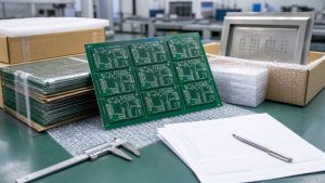
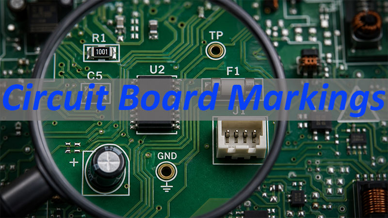
Circuit board markings are the letters, numbers, symbols, polarity signs, and reference codes printed on a PCB to help identify components, assembly direction, test points, safety areas, and possible defects. This guide explains how to read PCB symbols and codes, including component markings, polarity labels, fuse markings, burn marks, water marks, and common PCB inspection questions.
If you are sourcing trusted PCB or quality-focused PCBA services, unclear markings can create real problems during assembly, repair, inspection, and quality control. A small missing polarity mark or unreadable reference designator may lead to wrong component placement, delayed debugging, failed testing, or costly rework.
What problems do customers often face when circuit board markings are unclear?
- They cannot tell whether a mark is a label or a defect.
- They confuse component codes such as R, C, D, Q, U, J, F, and TP.
- They miss polarity marks and install parts in the wrong direction.
- They struggle to judge burn marks, scorch marks, or water marks.
- They receive boards with poor silkscreen readability.
A professional PCB and PCBA manufacturer helps prevent these issues before production starts.
- We review silkscreen clarity before PCB fabrication.
- We check reference designators against the BOM and assembly files.
- We verify polarity marks for capacitors, diodes, ICs, and connectors.
- We inspect abnormal burn marks, stains, and contamination.
- We keep PCB markings consistent for assembly, testing, and repair.
EBest Circuit (Best Technology) is a professional PCB and PCBA manufacturer supporting custom PCB prototype, quick PCB fabrication, component sourcing, PCB SMT assembly, through-hole assembly, engineering review, and quality inspection. We help customers improve PCB layout readability, silkscreen accuracy, component identification, polarity control, and production reliability. For PCB or PCBA manufacturing support, contact us at sales@bestpcbs.com.
What Are Circuit Board Markings?
Circuit board markings are the visual information printed, etched, labeled, or laser-marked on a PCB. They help engineers, assemblers, inspectors, and repair technicians understand what each component, pad, connector, and test point is used for.
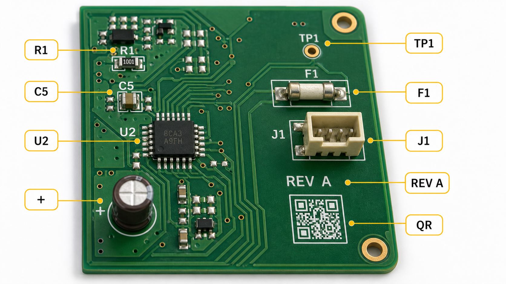
Most markings are printed on the silkscreen layer, but some may also appear as copper text, solder mask openings, adhesive labels, QR codes, barcodes, or laser marking.
Common circuit board markings include:
| Marking Type | Example | Purpose |
|---|---|---|
| Reference designator | R1, C5, U2 | Identify components |
| Polarity mark | +, -, dot, stripe | Show direction |
| Test point | TP1, TP2 | Support electrical testing |
| Fuse mark | F1, F2 | Identify protection parts |
| Connector mark | J1, CN1 | Show interface position |
| Revision code | REV A, V1.2 | Track design version |
These markings are not decoration. They connect the physical PCB to the schematic, BOM, assembly drawing, test procedure, and repair documentation.
In short, circuit board markings are the map of a PCB. Without them, assembly and troubleshooting become slower, riskier, and more expensive.
How to Read Circuit Board Markings Step by Step
To read circuit board markings correctly, start with the obvious labels first, then move to smaller component codes and polarity symbols. This helps you avoid confusing normal PCB markings with damage or contamination.
A practical reading process is:
- Find the board name, part number, or revision code.
- Identify major components, connectors, and power input areas.
- Read reference designators such as R, C, D, Q, U, J, F, and TP.
- Check polarity markings before removing or installing components.
- Compare the PCB markings with the schematic, BOM, and assembly drawing.
- Inspect abnormal areas such as burn marks, water marks, or corrosion.
- Confirm unclear markings with the manufacturer before repair or production.
For example, C12 usually means capacitor position 12. If the same footprint has a + mark, it may be a polarized capacitor and must be installed in the correct direction.
The safest approach is to read PCB markings together with technical files, not by visual guessing alone.
Common Printed Circuit Board Markings and What They Mean
Printed circuit board markings usually refer to the symbols and text printed on the silkscreen layer. These markings help identify components, orientation, test points, warnings, and manufacturing information.
Common printed circuit board markings include:
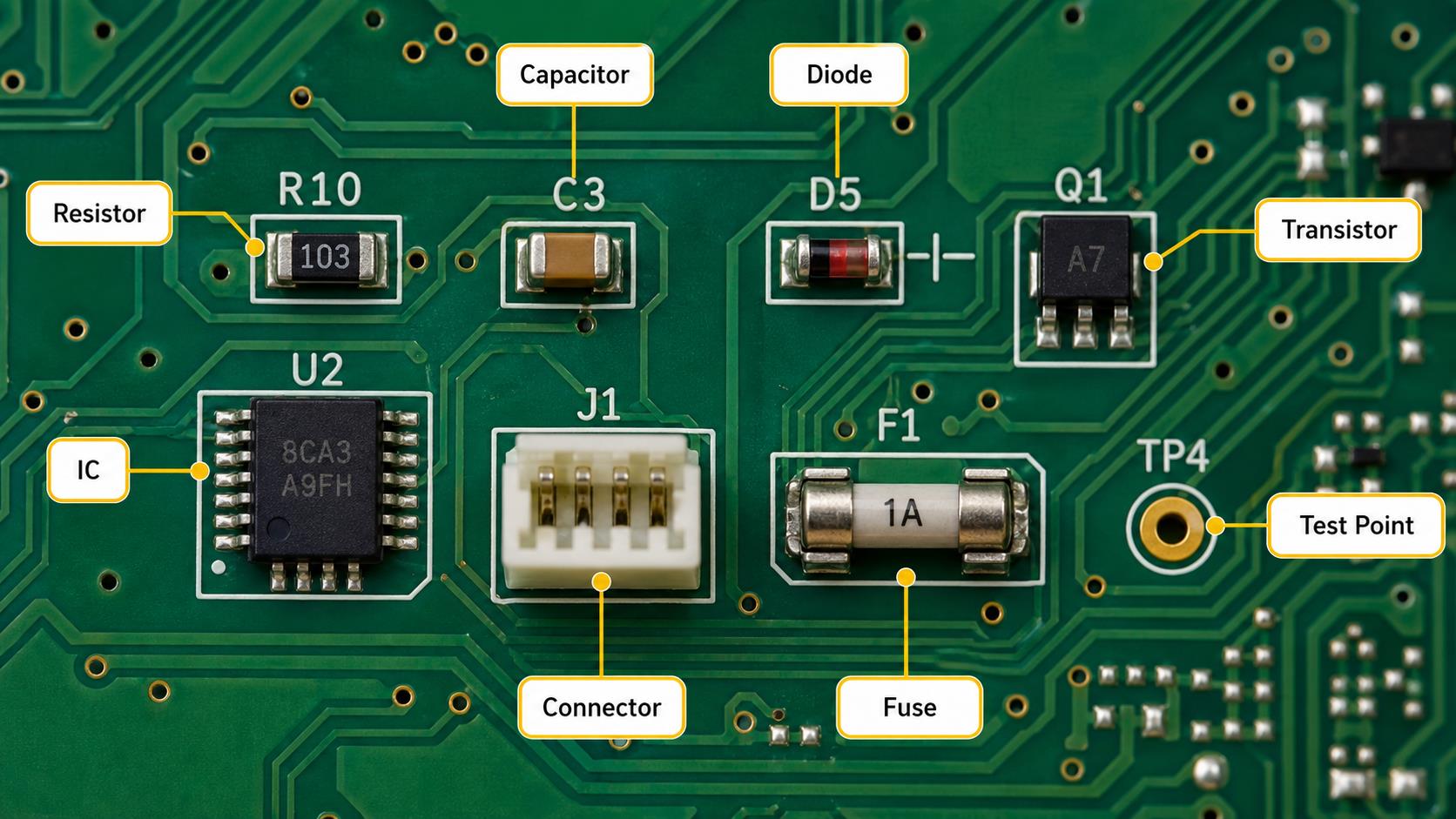
R: ResistorC: CapacitorD: Diode or LEDQ: Transistor or MOSFETUorIC: Integrated circuitJorCN: ConnectorF: FuseTP: Test pointSW: SwitchL: InductorGND: GroundVCC,VIN,5V,12V: Power net labels
Some PCBs also include UL marks, RoHS marks, date codes, lot codes, QR codes, or manufacturer identification. These are useful for traceability, compliance, and quality management.
For production, printed circuit board markings should be readable after soldering, cleaning, conformal coating, and final inspection. If the text is too small, too close to pads, or hidden under components, it may create assembly or repair problems.
Circuit Board Component Markings: R, C, D, Q, U, J, F, and TP
Circuit board component markings are usually reference designators. They do not always show the exact component value, but they tell you what type of component belongs in that position.
Here is a simple reference table:
| Marking | Component Type | Example |
|---|---|---|
| R | Resistor | R10 |
| C | Capacitor | C3 |
| D | Diode/LED | D5 |
| Q | Transistor/MOSFET | Q1 |
| U | IC/chip | U2 |
| J/CN | Connector | J1 |
| F | Fuse | F1 |
| TP | Test point | TP4 |
These component markings are important for SMT assembly, through-hole assembly, inspection, testing, and repair. During PCBA production, the assembler uses these reference designators together with the BOM and pick-and-place file.
If component markings are missing or inconsistent, technicians may need to trace the circuit manually. That can increase inspection time and raise the risk of assembly mistakes.
Clear circuit board component markings make the PCB easier to build, test, repair, and reproduce.
Circuit Board Capacitor Polarity Markings Explained
Circuit board capacitor polarity markings are important because polarized capacitors can fail if installed backward. Electrolytic capacitors and some tantalum capacitors are especially sensitive to polarity.
Common capacitor polarity markings include:
+mark for the positive pad- Shaded area or stripe for the negative side
- Square pad or special pad shape
- Silkscreen outline matching the capacitor body
- Longer lead on through-hole capacitors as positive
- Stripe on the capacitor body as negative
For PCBA production, capacitor polarity circuit board marking must match the BOM, assembly drawing, and component datasheet. If the PCB marking is unclear, the manufacturer should confirm orientation before mass production.
This is especially important for power supplies, LED drivers, motor control boards, battery systems, and industrial control PCBs.
In short, capacitor polarity markings help prevent reverse installation, overheating, leakage, and functional failure.
Polarity Markings on Circuit Boards: Positive, Negative, Diode, and IC Pin 1
Polarity markings on circuit boards show direction. They are critical for polarized components such as capacitors, diodes, LEDs, ICs, connectors, relays, batteries, and power input terminals.
Typical polarity markings include:
+for positive voltage.-for negative or ground.- Diode line mark for cathode direction.
- Dot, notch, or bevel for IC pin 1.
- Triangle or square pad for connector orientation.
- Battery symbols for positive and negative terminals.
Positive marks on circuit board areas are useful, but they should never be interpreted alone. Always check the complete footprint, nearby labels, schematic, and component datasheet.
For manufacturers, polarity control is a key part of PCBA quality. A reversed diode, capacitor, IC, or connector can cause immediate board failure.
Good polarity marking reduces assembly errors, improves inspection speed, and protects the final product from avoidable electrical failure.
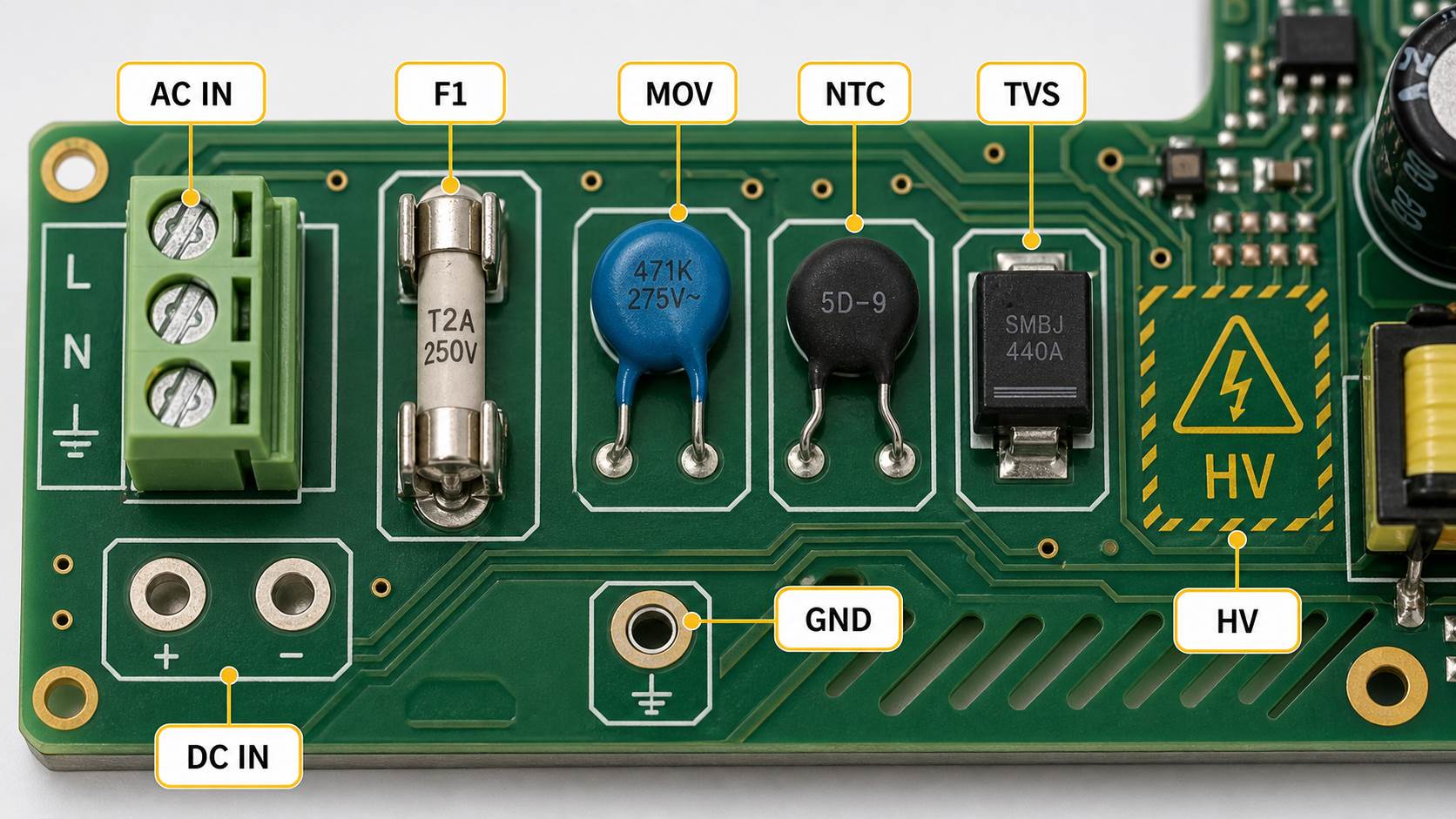
Circuit Board Fuse Markings and Other Safety Labels
Circuit board fuse markings help users identify protective components in power input, motor control, battery, industrial, automotive, and consumer electronic boards. Fuse markings usually appear as F1, F2, or similar labels.
Other safety-related PCB markings may include:
F: FuseMOV: Surge protection componentNTC: Inrush current limiterTVS: Transient voltage suppressorGND: GroundHV: High voltage warningAC IN: AC power inputDC IN: DC power input
These labels help technicians locate protection circuits quickly during inspection or repair. They also help separate low-voltage, high-voltage, input, output, and ground areas.
For PCB manufacturing, safety labels should not be placed too close to pads, covered by large components, or removed during cleaning. If conformal coating is used, markings should remain visible where inspection is required.
Clear fuse markings and safety labels make the PCB safer to handle and easier to diagnose.
Are Burn Marks on Circuit Board the Same as Circuit Board Markings?
Burn marks on circuit board surfaces are not normal circuit board markings. They usually indicate overheating, overload, short circuit, poor soldering, component failure, contamination, or long-term electrical stress.
Common signs include:
- Brown or black scorch marks
- Darkened solder mask
- Burnt smell around components
- Discolored copper pads
- Melted connector housing
- Charred areas near power components
A circuit board burn mark should not be treated as a printed label. If burn marks appear near fuses, MOSFETs, resistors, capacitors, connectors, or power traces, the board should be inspected carefully before reuse.
Do scorch marks affect a circuit board? They can. Even if the board still works, heat damage may weaken the substrate, copper adhesion, solder joints, or nearby components.
Intentional PCB markings help identify parts. Burn marks are warning signs that the board may need testing, repair, or replacement.
Water Marks on Circuit Board: What They Indicate and When to Worry
Water marks on circuit board surfaces may come from moisture, cleaning residue, flux residue, leakage, condensation, poor storage, or environmental exposure. Some marks are only cosmetic, but others may affect electrical reliability.
Watch for these signs:
- White residue near solder joints
- Green corrosion around copper
- Sticky or cloudy contamination
- Rust on shields or connectors
- Water stains near edge connectors
- Intermittent electrical failure
Water marks are more serious when they appear on powered boards, high-voltage areas, fine-pitch ICs, connectors, or dense SMT layouts. Moisture can cause leakage current, corrosion, dendrite growth, short circuits, and long-term reliability problems.
In PCB and PCBA production, cleaning, drying, packaging, and storage conditions all matter. A professional manufacturer should control contamination and inspect abnormal stains before shipment.
Water marks should be evaluated separately from normal printed circuit board markings because they may indicate contamination or environmental damage.
FAQs About Circuit Board Markings
Circuit board markings help users read PCB symbols, codes, polarity signs, component labels, safety labels, and possible defect indicators. Below are common questions about PCB markings.
What do circuit board markings mean?
They identify components, polarity, connectors, test points, fuses, revision codes, safety labels, and sometimes compliance or traceability information.
How do I read circuit board markings?
Start with the board part number and revision code. Then read reference designators such as R, C, D, Q, U, J, F, and TP. Finally, check polarity and safety markings.
What does C mean on a circuit board?C usually means capacitor. For example, C10 means capacitor position 10 on the PCB.
What does R mean on a circuit board?R usually means resistor. The number after it identifies the resistor position.
What do polarity markings on circuit boards show?
They show positive, negative, cathode, anode, or pin 1 direction for components that must be installed in a specific orientation.
Are burn marks on circuit board normal?
No. Burn marks usually indicate overheating, overload, short circuit, poor soldering, or component failure.
Can water marks on a circuit board cause failure?
Yes. Moisture or residue can cause corrosion, leakage current, short circuits, or intermittent failure.
What are circuit board fuse markings?
Fuse markings usually appear as F1, F2, or similar labels. They identify protective fuse positions on the PCB.
What is the difference between PCB silkscreen and laser marking?
Silkscreen is printed on the PCB surface, while laser marking is engraved or marked by laser for traceability, barcodes, QR codes, or permanent identification.
Can EBest Circuit help improve PCB markings before production?
Yes. EBest Circuit (Best Technology) can review PCB files, silkscreen readability, polarity marks, component designators, assembly drawings, and PCBA manufacturability before production.
To summarize, circuit board markings are essential visual guides that help users understand PCB symbols, component codes, polarity direction, test points, safety labels, and possible damage signs. This article explained how to read PCB symbols and codes, including printed circuit board markings, component markings, capacitor polarity markings, fuse markings, burn marks, and water marks.
EBest Circuit (Best Technology) supports custom PCB fabrication and PCBA assembly with engineering review, clear silkscreen control, polarity checking, component placement verification, testing, and quality inspection. If you need reliable PCB or PCBA manufacturing support, pls feel free to contact us at sales@bestpcbs.com.