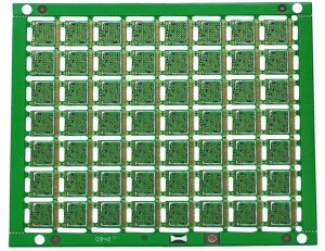
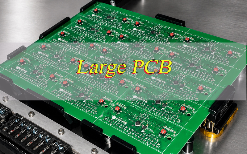
A large PCB is a circuit board with dimensions beyond common production or assembly handling ranges. It is used in industrial control, LED display, power electronics, telecom equipment, testing systems and large electronic modules.
Compared with a standard board, it requires better flatness control, copper balance, drilling accuracy, material stability and assembly support. For buyers, the real challenge is not size alone. The board must stay reliable during fabrication, assembly, testing, shipment and final installation.
Are you worried about these problems in large PCB projects?
- Design risk: Unbalanced copper, weak support points, unsuitable thickness or poor connector layout may cause bending, cracking or installation stress.
- Production risk: Oversized panels may face uneven plating, solder mask defects, dimensional deviation, routing stress and longer production cycles.
- Assembly risk: Long boards may bend during printing, placement, reflow, inspection or final testing without stable fixture support.
As a PCB manufacturer with 20+ years of experience, EBest Circuit helps global OEM factories, engineering companies and industrial equipment brands turn complex large PCB designs into stable production. Below are our solutions to these above challenges of large PCB board:
- Free DFM review before production: We review board size, stack-up, copper weight, material, drill design, panel direction and connector layout to reduce design mistakes before fabrication starts.
- Controlled large PCB manufacturing: We focus on copper balance, plating uniformity, solder mask coverage, dimensional tolerance and flatness control to improve production stability and batch consistency.
- Reliable assembly and testing support: We check BOM, CPL, stencil design, component height, fixture needs and testing requirements to reduce soldering defects, board deformation and rework risk.
Welcome to contact us if you have any request for large PCB manufacturing and assembly: sales@bestpcbs.com.
What Is a Large PCB Board?
A large PCB board is a printed circuit board with a size larger than normal production or assembly handling capability. It may also be called an oversized PCB, large format PCB or large size PCB board.
This term refers to board dimensions, not order quantity. A project can be one sample and still require special production control if the outline is long, wide, thick or hard to handle.
Reliability is the main concern. Bigger boards are more sensitive to material expansion, copper imbalance, bending force and shipping damage. For this reason, both electrical design and mechanical support should be reviewed before production.
What Applications Commonly Use Large Size PCB Boards?
Large size PCB boards are used when one continuous circuit area can reduce cables, connectors and mechanical complexity. They are common in products with wide layout space, long current paths or large installation structures.
Common large PCB applications include:
- Industrial control equipment: motor drives, power control modules, control cabinets and automation systems.
- LED display systems: display panels, long lighting modules and outdoor signage boards.
- Power electronics: UPS systems, inverters, charging equipment and high-current controllers.
- Telecom equipment: backplanes, antenna control modules and communication power boards.
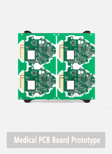
- Medical equipment: diagnostic machines, imaging platforms and large control modules.
- Testing systems: inspection fixtures, laboratory instruments and burn-in platforms.
In these projects, stable size, strong support and controlled assembly matter more than simply making a bigger circuit board.
What Size Range Can Large PCB Fabrication Support?
Large PCB fabrication capability depends on equipment size, material type, layer count, copper weight, board thickness and tolerance level. A two-layer oversized board is usually easier to manufacture than a large multilayer board with heavy copper and tight registration.
| Item | Typical Range |
|---|---|
| Standard panel | 457 × 610 mm |
| Oversized range | 500 × 600 mm to 600 × 1200 mm |
| Board thickness | 1.6 mm to 4.0 mm |
| Heavy copper | 3 oz to 10 oz+ |
| Layer count | 1 to 20+ layers |
| Line tolerance | Project-based review |
| Bow/twist target | ≤0.75% for many SMT boards |
| Testing | 100% electrical test recommended |
Maximum size PCB fabrication must be confirmed with Gerber files. Slots, cutouts, copper coverage, drill density, surface finish and assembly process may reduce the practical size limit.
What Are the Main Challenges in Large PCB Manufacturing?
Large PCB manufacturing is more difficult because size increases stress, handling difficulty and process variation.
- Board warpage: Long or wide boards may bend during lamination, curing, reflow or storage if copper balance and thickness are not well controlled.
- Dimensional deviation: Oversized panels are more affected by material expansion, routing stress and drilling position shift.
- Uneven copper plating: A larger board area can make current distribution harder to control, especially for heavy copper or dense hole designs.
- Solder mask defects: Large surface areas may increase the risk of uneven coating, poor edge coverage, misalignment or weak adhesion.
- Hole wall reliability: Thick or large boards require stable drilling, desmear and plating control to keep plated through holes reliable.
- Handling damage: Large boards are easier to scratch, bend or damage at corners during production, inspection, packing and shipment.
- Assembly deformation: If the board is long, thin or heavy, it may bend during SMT printing, component placement and reflow.
The main goal is to control flatness, copper balance, hole quality and safe handling from the beginning of production.
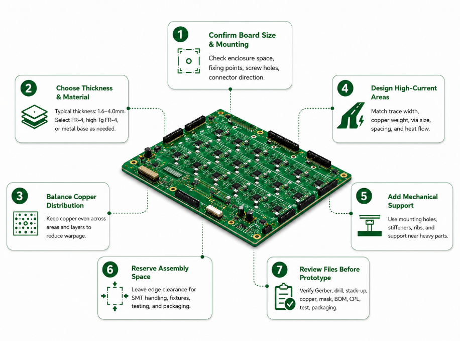
How to Design a Large PCB for Stable Performance?
Step 1: Confirm board size and installation method.
Start with the final product structure. Check the available installation space, fixing method, screw hole position, connector direction and mechanical support. A large PCB should be designed for the real enclosure, not only for the circuit layout.
Step 2: Select suitable thickness and material.
A long or wide board usually needs stronger rigidity. Common thickness choices include 1.6 mm, 2.0 mm, 2.4 mm, 3.2 mm and 4.0 mm, depending on size, copper weight and component loading. FR-4 is suitable for general use, while high Tg FR-4 or metal base material may be better for heat or power applications.
Step 3: Balance copper distribution.
Avoid placing heavy copper only on one side or one local area. Uneven copper can pull the board during lamination and heat processing. For multilayer designs, copper planes should be as balanced as possible between layers.
Step 4: Design high-current areas carefully.
For power circuits, use proper trace width, copper weight, via size and spacing. Heavy copper can improve current carrying capacity, but it also requires larger spacing and better etching control. Heat flow should be reviewed together with the copper layout.
Step 5: Add mechanical support.
Use mounting holes, stiffeners, support ribs or fixing points when the board is long or carries heavy components. Terminals, transformers, relays and connectors should be placed near supported areas when possible.
Step 6: Reserve assembly and handling space.
Leave enough board edge clearance for SMT conveyors, fixtures, testing tools and packaging. If the board is too close to its outline limit, assembly handling may become unstable.
Step 7: Review files before prototype production.
Before large PCB prototype production, check Gerber files, drill files, stack-up, copper weight, solder mask, BOM, CPL, testing method and packaging needs. This helps reduce rework before mass production.
What Thickness Is Suitable for a Large Size PCB Board?
Thickness should match board size, component weight, copper weight and mounting method. A thin oversized board may bend during SMT or transportation, while an overly thick board may increase cost and drilling difficulty.
| Application | Common Thickness |
|---|---|
| Control board | 1.6 mm |
| Industrial board | 2.0 mm to 2.4 mm |
| Heavy component board | 2.4 mm to 3.2 mm |
| Power board | 2.0 mm to 3.2 mm |
| Heavy copper board | 2.4 mm to 4.0 mm |
| Backplane | Project-based design |
For large custom PCB panel thickness, the best choice should be reviewed with outline size, copper weight and mounting structure. A balanced design is usually more reliable than simply choosing the thickest board.
How Does Copper Thickness Affect Large PCB Fabrication?
Copper thickness affects current capacity, temperature rise, etching accuracy, solder mask coverage and final flatness. For power equipment, heavy copper can improve current carrying ability and heat spreading.
| Copper Weight | Common Use |
|---|---|
| 1 oz | Signal and control circuits |
| 2 oz | Medium current circuits |
| 3 oz | Entry-level heavy copper |
| 4 oz to 6 oz | Industrial power boards |
| 8 oz to 10 oz+ | High-current custom boards |
However, thicker copper also makes production harder. It requires wider spacing, better etching compensation and stricter plating control. If copper is concentrated in one area, the board may bend during lamination or reflow.
Heavy copper large PCB fabrication should always review copper balance, minimum spacing, hole copper and heat requirements together.
What Materials Are Commonly Used for Large Format PCB Boards?
Large format PCB boards commonly use FR-4, high Tg FR-4, aluminum base, copper base or RF laminates. Material selection should match working temperature, current load, mechanical support and product environment.
| Material | Suitable Use |
|---|---|
| FR-4 | General industrial boards |
| High Tg FR-4 | Higher heat resistance |
| Aluminum base | LED and heat dissipation |
| Copper base | High-power heat design |
| Rogers material | RF and high-frequency circuits |
| Heavy copper FR-4 | Power electronics |
| Halogen-free FR-4 | Environmental compliance |
FR-4 is the most common material because it offers balanced cost and performance. High Tg material is better for multilayer structures or products exposed to repeated heat.
For LED, inverter or high-power designs, metal base materials may help with heat transfer. The final material should be selected by working environment, not only by board size.
What Should Be Checked Before Large PCB Prototype Production?
Before large PCB prototype production, the design should be checked for fabrication, assembly, testing and packaging. This step helps avoid expensive rework before batch production.
Before production, review:
- Gerber files: outline, copper layers, drill data, slots, solder mask and silkscreen.
- Stack-up: layer count, dielectric thickness, copper weight and material grade.
- Board outline: size, cutouts, routing path and fixture space.
- Copper balance: large copper areas, heavy copper zones and plane symmetry.
- Hole design: drill size, annular ring, plated holes and aspect ratio.
- Assembly data: BOM, CPL, polarity, connector direction and component height.
- Testing plan: electrical test, AOI, functional test and inspection standard.
- Packaging plan: board separation, corner protection and moisture control.
A complete review improves first-pass success and makes later production more predictable.
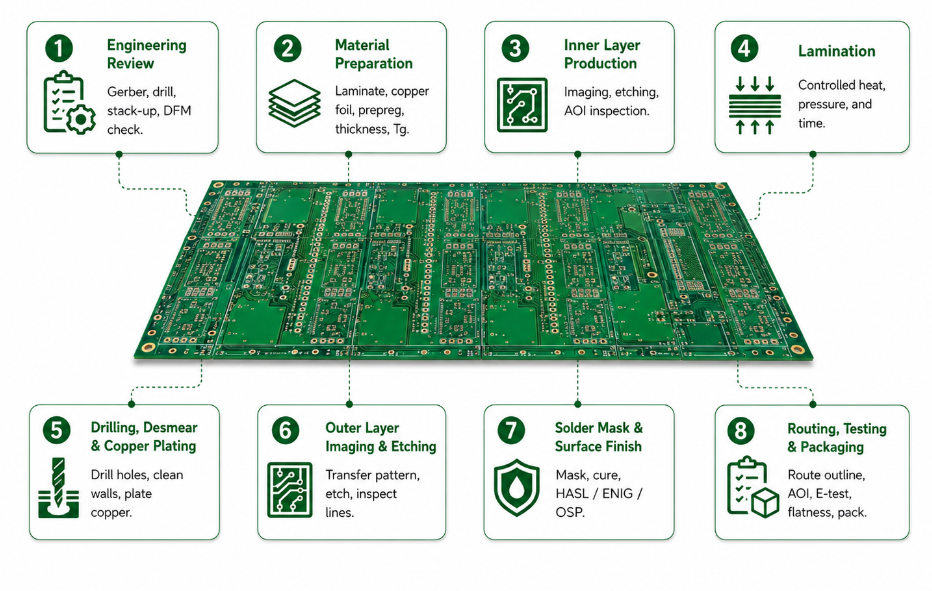
How Is a Large PCB Manufactured Step by Step?
Step 1: Engineering review.
Production starts with Gerber, drill file and stack-up review. The factory checks board size, material, copper weight, thickness, hole design, spacing, surface finish, tolerance and assembly requirements. If warpage or copper balance risk is found, DFM feedback is given before production.
Step 2: Material preparation.
The laminate, copper foil and prepreg are prepared according to the confirmed specification. For oversized boards, material thickness, Tg, copper weight and cutting direction must be controlled to reduce stress during later processes.
Step 3: Inner layer production.
For multilayer boards, inner layers are imaged, etched and inspected first. AOI is used to check opens, shorts, line width and spacing before lamination. Any inner layer defect should be removed before the board is pressed.
Step 4: Lamination.
Inner layers, prepreg and copper foil are pressed together under controlled temperature, pressure and time. Large boards are more sensitive to heat and pressure changes, so lamination stability directly affects flatness and dimensional accuracy.
Step 5: Drilling, desmear and copper plating.
After lamination, holes and slots are drilled. The hole walls are cleaned by desmear, then plated with copper to create electrical connection between layers. For thick or heavy copper boards, hole wall quality must be checked carefully.
Step 6: Outer layer imaging and etching.
The outer circuit pattern is transferred and etched. Heavy copper designs need proper etching compensation because thicker copper is harder to control. Line width, spacing and copper residue should be inspected after etching.
Step 7: Solder mask and surface finish.
Solder mask is applied, exposed and cured. The process must control coverage, adhesion and alignment. Then the selected surface finish, such as HASL, ENIG or OSP, is applied according to assembly and storage requirements.
Step 8: Routing, testing and packaging.
The board outline, slots and cutouts are routed. After that, the board goes through AOI, electrical testing, dimensional inspection, flatness review and visual inspection. Finally, reinforced packaging is used to reduce bending, scratches and corner damage during shipment.
What Is the Difference Between Standard PCB and Large PCB Fabrication?
The difference is not only size. Standard boards mainly focus on circuit accuracy, drilling quality, solder mask and electrical testing. Large PCB fabrication must also control mechanical stress, board support, flatness and packaging safety.
| Item | Standard PCB | Oversized PCB |
|---|---|---|
| Size risk | Low | High |
| Warpage risk | Lower | Higher |
| Copper balance | Important | Critical |
| Plating control | Easier | More difficult |
| Routing stress | Lower | Higher |
| SMT handling | Standard support | Fixture may be used |
| Packaging | Normal carton | Reinforced protection |
| Cost driver | Layers and quantity | Size, yield and handling |
A standard board may pass with normal handling, but an oversized board can fail because of bending or deformation. That is why factory experience and engineering review matter.
How Does Large Format PCB Assembly Work?
Step 1: Assembly file review.
The assembly team checks BOM, CPL, Gerber files, stencil design, component height, polarity, connector direction and testing requirements. This review confirms whether the board can pass printing, placement, reflow and inspection smoothly.
Step 2: Fixture and support planning.
Large format PCB assembly often needs extra support under the board. If the board is long, thin or heavy, fixtures may be prepared for solder paste printing, SMT placement, reflow and testing.
Step 3: Solder paste printing.
The board must stay flat during stencil printing. If the board bends, solder paste thickness may become uneven and cause bridging, insufficient solder or open joints.
Step 4: SMT component placement.
Components are placed according to the CPL file. Placement accuracy must remain stable across the full board area. Heavy components and tall connectors should be reviewed for handling and support.
Step 5: Reflow soldering.
The assembled board passes through a controlled reflow profile. Heat rise, peak temperature and cooling rate should be suitable for the board size, material and component mix. Stable support helps reduce bending during reflow.
Step 6: Through-hole and selective soldering.
If the design includes connectors, terminals or power components, through-hole soldering or selective soldering may be used after SMT. These areas should be checked for solder filling, wetting and mechanical strength.
Step 7: Inspection and functional testing.
AOI checks solder joints, polarity, missing parts and alignment. X-ray inspection may be used for hidden joints such as BGA or power packages. Functional testing verifies whether the assembled board works as required.
Step 8: Final cleaning and packaging.
After inspection, the board is cleaned if required and packed with proper support. Oversized PCB assembly services should include packaging protection to reduce bending and damage during transport.
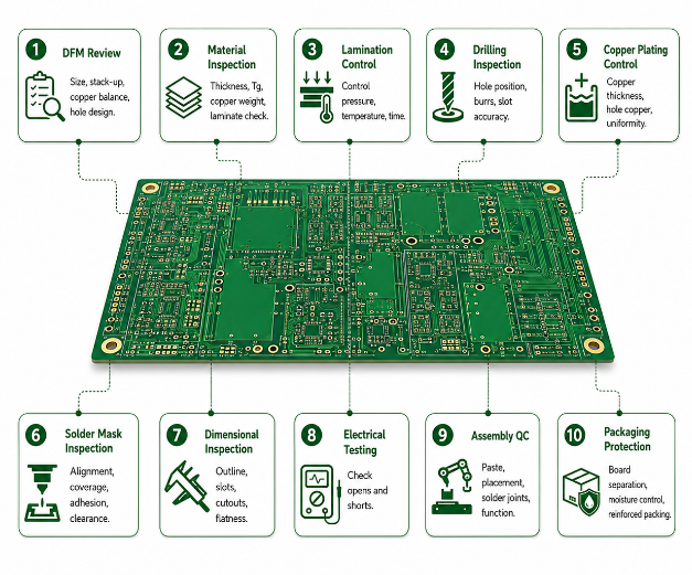
How Do We Ensure Quality in Large PCB Manufacturing?
- DFM review before production: We review board size, stack-up, copper balance, material, hole design, surface finish, testing needs and assembly risk before fabrication starts.
- Material inspection: We check material type, thickness, Tg, copper weight and laminate condition to make sure the board matches the confirmed specification.
- Lamination control: We control pressure, temperature and time to reduce internal stress, layer shift and warpage.
- Drilling inspection: We check hole position, drill quality, burrs, slot accuracy and hole wall condition before plating.
- Copper plating control: We inspect copper thickness, hole copper and plating uniformity, especially for heavy copper and high-current boards.
- Solder mask inspection: We check solder mask alignment, coverage, adhesion, exposure quality and clearance around pads.
- Dimensional inspection: We measure outline size, slots, cutouts, hole position and flatness according to project requirements.
- Electrical testing: We use electrical testing to check opens and shorts before shipment.
- Assembly quality control: For PCBA orders, we check solder paste printing, component placement, solder joints, connector strength and functional performance.
- Packaging protection: We use board separation, corner protection, moisture control and reinforced packing to reduce bending and transport damage.
Our quality control focuses on prevention, not only final inspection. This helps large PCB boards stay stable from prototype to batch production.
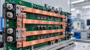
Case Study: Heavy Copper Oversized PCB for Industrial Power Equipment
Project Background
A customer needed an oversized heavy copper board for industrial power equipment. The product worked in a high-current environment and required stable power transmission, good heat spreading and strong mechanical support. The board also included terminal blocks and heavy components, so bending and solder joint stress were major concerns.
Customer Requirements
The customer required a large board outline, heavy copper areas, reliable plated through holes and stable assembly performance. The board had to support high current, reduce local heat rise and remain flat during production and reflow. The customer also needed a prototype that could move smoothly into batch production after validation.
Our Solution
EBest PCB reviewed the stack-up, copper balance, board thickness, spacing, hole copper and terminal layout before production. We found that some power zones had much higher copper coverage than other areas, which could increase deformation risk. Therefore, we adjusted the DFM suggestions, strengthened plating control, checked solder mask clearance and prepared reinforced handling during assembly.
Final Results
The finished board achieved stable current carrying capacity, improved heat distribution and better mechanical reliability. The sample passed customer validation and moved to batch production. This project showed that heavy copper large PCB fabrication should combine electrical design, heat control, flatness management and assembly support from the start.
What Large PCB Manufacturing Services Can EBest PCB Provide?
EBest PCB provides one-stop support for large PCB projects, from engineering review to finished PCB assembly. This helps customers reduce supplier communication, shorten project transfer time and control production risk.
- PCB design review: We review board size, stack-up, copper balance, material, drill design and assembly risk before production.
- Large PCB prototype: We support sample production for oversized PCB, heavy copper PCB, multilayer PCB and special material boards.
- Mass production: We support batch production with a monthly capability of 260,000 square feet / 28,900 square meters.
- Component sourcing: We help prepare components based on customer BOM requirements for PCBA orders.
- PCB assembly: We provide SMT assembly, through-hole assembly, connector soldering, functional testing and final inspection.
- Expedited service: For suitable urgent boards, shipment can be supported within 24 hours after production details are confirmed.
Our product capability covers FR4 PCB, multilayer PCB, metal core PCB, ceramic PCB, flexible PCB, rigid-flex PCB, high frequency PCB, heavy copper PCB, HDI PCB, high Tg PCB and impedance control PCB.
Why Choose EBest PCB as Large PCB Manufacturer in China?
Choosing EBest PCB helps customers reduce design risk, save communication time and move from prototype to production with stronger control.
- Lower project risk: With 20+ years of PCB experience, our team can review large board risks before production, including warpage, copper balance, thickness, hole design and assembly handling.
- Faster project transfer: PCB design review, prototype, mass production, component sourcing and PCB assembly can be handled through one supplier, reducing repeated communication between different vendors.
- Stronger production support: With monthly capability of 260,000 square feet / 28,900 square meters, we can support both sample verification and batch orders.
- More material choices: Customers can choose FR4, high Tg FR4, metal core, ceramic, flexible, rigid-flex, high frequency and heavy copper structures according to project needs.
- Better compliance support: Certifications including IATF 16949, ISO 9001:2015, ISO 13485:2016, AS9100D, REACH, RoHS and UL help support automotive, medical, aerospace, industrial and general electronics projects.
- Clearer delivery path: Expedited service is available for suitable urgent boards, helping customers handle tight project schedules.
For buyers, the value is simple: one China source factory, fewer project delays, clearer engineering support and more stable production control.
FAQs About Large PCB Boards
Q1: What files should I send for a large PCB quote?
A1: Please send Gerber files, drill files, board thickness, copper weight, material, surface finish, quantity and delivery request. For PCBA orders, also send BOM, CPL and testing requirements. Complete files help shorten quotation time and reduce production misunderstanding.
Q2: Can EBest PCB help review my design before production?
A2: Yes. EBest PCB can review board size, stack-up, copper balance, hole design, spacing, material and assembly risk before production. This helps customers find manufacturability problems before they become prototype or batch defects.
Q3: Can I start with samples before mass production?
A3: Yes. You can start with large PCB prototype production to verify size, flatness, copper performance, soldering and function. After sample approval, the project can move to batch production with confirmed process settings.
Q4: Can EBest PCB source components for PCBA orders?
A4: Yes. EBest PCB supports component sourcing based on customer BOM requirements. This helps customers reduce purchasing workload and keep PCB fabrication, component preparation and assembly in one project flow.
Q5: How fast can urgent boards be delivered?
A5: For suitable urgent boards, EBest PCB can support expedited service, and some boards can be shipped within 24 hours after all files, materials and production details are confirmed. Actual timing depends on board structure and process difficulty.
Q6: What certifications does EBest PCB have?
A6: EBest PCB is supported by IATF 16949, ISO 9001:2015, ISO 13485:2016, AS9100D, REACH, RoHS and UL. These certifications help customers meet project requirements in automotive, medical, aerospace, industrial and electronic products.
Q7: What PCB types can EBest PCB manufacture?
A7: EBest PCB can manufacture FR4 PCB, multilayer PCB, metal core PCB, ceramic PCB, flexible PCB, rigid-flex PCB, high frequency PCB, heavy copper PCB, HDI PCB, high Tg PCB and impedance control PCB.
Q8: Is EBest PCB a factory or a trading company?
A8: EBest PCB is positioned as a China source factory for custom PCB and PCBA solutions. Customers can work with one team for design review, prototype, mass production, component sourcing and PCB assembly.
Q9: Can EBest PCB support regulated industry projects?
A9: Yes. With certifications such as IATF 16949, ISO 13485:2016 and AS9100D, EBest PCB can support projects in automotive, medical, aerospace and industrial fields. Final requirements should be confirmed by customer drawings and specifications.
Q10: How can I reduce risk before placing a batch order?
A10: Start with complete files, request design review, build samples, test the board and confirm assembly performance before mass production. This process is safer for oversized boards because size, flatness and handling risks can be checked early.
A reliable large PCB project needs early design review, suitable material selection, stable fabrication, controlled assembly and clear delivery planning. EBest Circuit helps customers reduce production risk through PCB design review, prototype support, mass production, component sourcing and PCB assembly from our China source factory.
Send your Gerber files, BOM, quantity and technical requirements to sales@bestpcbs.com. Our team will review your large PCB project and provide a practical quotation for manufacturing and assembly.