PCB manufacturing PCB manufacturing
Home > Blog

Top 10 Largest Printed Circuit Board Manufacturers in China

July 7th, 2026

Largest printed circuit board manufacturers in China are PCB companies with strong production scale, advanced process capability, stable quality systems, and broad customer coverage. This article explains how large PCB manufacturers are ranked, lists 10 major PCB companies in China, and shows how buyers can choose between large-volume PCB makers and custom PCB manufacturers.

Why do buyers search for the largest printed circuit board manufacturers before sending an RFQ?

  • They do not know which PCB company is truly reliable.
  • They worry that small suppliers cannot handle complex PCB requirements.
  • They see many “top PCB manufacturers” lists but no clear comparison logic.
  • They are unsure whether a large PCB factory accepts prototype or custom projects.
  • They need proof: certifications, capacity, PCB types, PCBA support, and overseas service.

A better supplier selection process should connect company size with real project fit.

  • Check ranking factors, not only company names.
  • Compare PCB types, process limits, certifications, and lead time.
  • Decide whether the project needs high-volume production or flexible customization.
  • Review PCBA, component sourcing, and testing capability when needed.
  • Choose a PCB manufacturer that matches the product stage and technical risk.

EBest Circuit (Best Technology) is a China-based PCB and PCBA manufacturer supporting custom PCB fabrication, PCB prototype, mass production, component sourcing, PCB assembly, and turnkey PCB solutions. Our capabilities cover FR4 PCB, Metal Core PCB, Ceramic PCB, HDI PCB, flexible PCB, rigid-flex PCB, high-frequency PCB, heavy copper PCB, and PCBA. For project review or quotation, contact sales@bestpcbs.com.

Largest Printed Circuit Board Manufacturers

What Does “Largest Printed Circuit Board Manufacturers” Mean?

The largest printed circuit board manufacturers are usually judged by revenue, production capacity, customer base, factory scale, technical capability, and global supply coverage. However, “largest” does not always mean “best for every project.”

A company may be very large because it serves smartphone, server, automotive, telecom, or AI hardware programs. That does not automatically mean it is the best choice for a small-batch ceramic PCB, an urgent prototype, or a custom PCBA order.

Ranking FactorWhy It Matters
RevenueMarket scale
CapacityVolume support
PCB TypesTechnical range
CertificationsQuality proof
CustomersIndustry trust
Overseas SupportExport readiness

The global PCB market is large and still growing. ResearchAndMarkets estimated the PCB market at $67.9 billion in 2023 and projected it to reach $92.4 billion by 2029, which explains why buyers pay close attention to major PCB manufacturing regions and large suppliers.

For buyers, the practical meaning is simple: use “largest” as a starting point, not the final decision.

Largest Printed Circuit Board Manufacturers

How Are the Largest PCB Manufacturers in China Ranked?

The largest PCB manufacturers in China can be ranked in different ways. Some lists focus on revenue. Others focus on output, factory area, domestic ranking, global ranking, or a specific product category such as HDI PCB, FPC, IC substrate, server PCB, or automotive PCB.

A clean ranking method should include:

  • Business scale: revenue, capacity, and customer base.
  • Product capability: multilayer PCB, HDI PCB, FPC, rigid-flex PCB, heavy copper PCB, high-frequency PCB.
  • Quality system: ISO, IATF, AS9100, UL, RoHS, REACH, or medical-related systems.
  • Industry coverage: automotive, communication, data center, medical, industrial, consumer electronics.
  • Engineering support: DFM, stack-up review, impedance control, PCBA, testing, and overseas service.

This is why PCB manufacturer ranking should not be read like a simple winner list. A high-volume factory may be excellent for server boards but less flexible for small custom projects. A custom PCB manufacturer may not be the largest, but it may provide better engineering response, MOQ flexibility, and special-board support.

Top 10 Largest Printed Circuit Board Manufacturers in China

The following list is a practical B2B reference of large and well-known printed circuit board manufacturers in China. The order may vary by year, revenue source, and ranking method, so buyers should use it as a supplier research starting point rather than a fixed audited ranking.

CompanyStrong AreaBest Fit
Shennan CircuitsPCB + IC substrateHigh-reliability electronics
Dongshan Precision / MultekPCB, FPC, rigid-flexHigh-density projects
Victory Giant TechnologyAI server PCBHigh-speed, high-volume
KinwongMultilayer PCBGlobal PCB supply
WUS Printed CircuitServer, AI, automotiveHPC and data center
Suntak TechnologyMultilayer, HDILarge-volume PCB
Aoshikang TechnologyHigh-precision PCBServer, auto, telecom
Fastprint Circuit TechPrototype, small batchEngineering projects
Founder PCBMultilayer, HDICommunication, smart devices
Guangdong EllingtonDouble-sided, multilayerHigh-density PCB
  • Shennan Circuits: Its core business covers printed circuit boards, packaging substrates, and electronic assembly, making it one of China’s more technology-driven PCB companies.
  • Dongshan Precision / Multek: Multek supports rigid PCB, FPC/FPCA, PCB, and rigid-flex products. Its rigid PCB capability includes high-layer-count and HDI structures.
  • Victory Giant Technology: Victory Giant is recognized as a major Chinese PCB manufacturer and is strongly associated with AI server and high-performance computing PCB demand.
  • Kinwong: Kinwong reported 2024 annual revenue of $1.762 billion and describes itself as one of the world’s largest printed circuit board suppliers.
  • WUS Printed Circuit: WUS manufactures PCBs for high-speed servers, accelerator modules, automotive domain controllers, AI, HPC, autonomous driving, medical, industrial, and navigation applications.
  • Suntak Technology: Suntak reports large annual capacity and positions itself as a listed high-tech company producing circuit boards for communications, servers, computers, medical electronics, industrial HDI, automotive electronics, mobile phones, and optoelectronics.
  • Aoshikang Technology: Aoshikang focuses on R&D, production, and sales of high-precision PCBs used in data centers, servers, automotive electronics, communications, and consumer electronics.
  • Fastprint Circuit Tech: Fastprint is headquartered in Shenzhen, listed on the Shenzhen Stock Exchange, and operates manufacturing campuses in Guangzhou, Yixing, and the UK.
  • Founder PCB: Founder PCB is a PCB company headquartered in Zhuhai, Guangdong, with a long operating history in multilayer and HDI PCB manufacturing.
  • Guangdong Ellington: Guangdong Ellington focuses on high-precision, high-density double-sided and multilayer printed circuit boards.
Largest Printed Circuit Board Manufacturers

Why Are Many of the Largest PCB Manufacturers Based in China?

Many of the largest PCB manufacturers are based in China because China has a complete electronics manufacturing ecosystem. PCB production depends on copper foil, laminate, drilling, plating, imaging, solder mask, surface finish, SMT, components, testing, packaging, and export logistics. China has dense supply-chain support for each step.

China’s PCB manufacturing advantage usually comes from:

  • Strong electronics supply chains in the Pearl River Delta and Yangtze River Delta.
  • Large demand from communication, automotive, consumer electronics, AI servers, and industrial equipment.
  • Mature support for PCB materials, surface treatment, mechanical processing, and assembly.
  • Wide factory choices, from high-volume PCB manufacturers to custom PCB manufacturers.
  • Strong export experience for overseas electronics companies.

For buyers, this means China is not only a low-cost PCB sourcing region. It is also a technical manufacturing hub with large printed circuit board manufacturers, prototype PCB manufacturers, PCBA service providers, and special PCB factories.

Large PCB Manufacturers vs Custom PCB Manufacturers in China

Large PCB manufacturers and custom PCB manufacturers serve different needs. The largest printed circuit board manufacturers in China are often strong in scale, automation, large customers, and stable high-volume production. Custom PCB manufacturers are often more flexible in special boards, engineering support, prototype orders, and communication.

Supplier TypeBest ForPossible Limitation
Large PCB manufacturersHigh-volume productionLess flexible MOQ
Custom PCB manufacturersSpecial PCB projectsSmaller scale
Prototype PCB manufacturersFast engineering samplesLimited mass volume
PCBA manufacturersFinished assembliesNeeds BOM clarity

A large factory is a good choice when the project has stable design files, large demand, and clear process requirements. A custom printed circuit board manufacturer is often better when the project needs HDI PCB, ceramic PCB, Metal Core PCB, heavy copper PCB, rigid-flex PCB, impedance control, unusual thickness, special materials, or PCBA support.

The right question is not “Which PCB manufacturer is the largest?” The better question is: “Which manufacturer fits this product?”

What PCB Types Do Top Printed Circuit Board Manufacturers in China Produce?

Top printed circuit board manufacturers in China usually produce a wide range of PCB types. The exact capability depends on each factory’s equipment, process control, materials, certifications, and target markets.

PCB TypeTypical Application
FR4 PCBGeneral electronics
Multilayer PCBIndustrial, telecom
HDI PCBCompact devices
Flexible PCBWearables, modules
Rigid-Flex PCBSpace-limited products
Metal Core PCBLED, power modules
Ceramic PCBHigh heat, power
Heavy Copper PCBHigh-current systems
High-Frequency PCBRF, communication
PCBAFinished assemblies

Large China PCB manufacturers often focus on high-volume multilayer boards, HDI boards, server boards, automotive boards, or consumer electronics. Custom PCB manufacturers may support more specialized structures, smaller quantities, or faster engineering feedback.

For buyers, PCB type is a key filter. A supplier strong in mobile-phone HDI may not be the best option for ceramic PCB. A factory strong in heavy copper may not be ideal for fine-pitch rigid-flex. The PCB type should guide supplier selection before price comparison begins.

How EBest Circuit Supports Custom PCB and PCBA Manufacturing

EBest Circuit (Best Technology) is not positioned only as one of the largest printed circuit board manufacturers by revenue. Its value is stronger for customers who need custom PCB fabrication, special PCB technologies, PCB prototype, mass production, component sourcing, PCB assembly, and turnkey support.

EBest Circuit CapabilityProof Point
Industry Experience20+ years
PCB Capacity260,000 sq ft/month
Board Variety1,000+ types/month
Countries Served40+
Delivery Record97% on-time delivery
CertificationsISO, IATF, AS9100D, UL

EBest Circuit supports FR4 PCB, Metal Core PCB, Ceramic PCB, HDI PCB, flexible PCB, rigid-flex PCB, high-frequency PCB, heavy copper PCB, PCB prototype, mass production, component sourcing, and PCB assembly. The company also holds ISO 9001:2015, ISO 13485:2016, IATF 16949, AS9100D, UL, REACH, and RoHS certifications.

This makes EBest Circuit suitable for buyers who need more than a commodity PCB supplier. If your project involves custom board structure, thermal design, special materials, PCBA assembly, or overseas communication, EBest Circuit can support the project from PCB review to finished delivery.

How to Compare the Largest PCB Manufacturers in China

When comparing the largest PCB manufacturers in China, do not compare only the company name. Compare the project fit.

Use this simple checklist:

  • PCB type: FR4, HDI, FPC, rigid-flex, Metal Core, Ceramic, heavy copper, high-frequency.
  • Technical limits: layers, line width/space, hole size, copper thickness, impedance, board thickness.
  • Quality proof: ISO, IATF, AS9100D, ISO 13485, UL, RoHS, REACH.
  • Order type: prototype, low volume, medium volume, high volume.
  • Support scope: PCB only, PCB + PCBA, sourcing, testing, box build.
  • Lead time: normal lead time, urgent order support, sample response.
  • Communication: English support, engineering feedback, quotation clarity.

The largest PCB manufacturer may be excellent for one program but unsuitable for another. A server PCB project may need high-layer-count and high-speed material capability. A medical device PCB may need ISO 13485-related quality control. A power module may require heavy copper, Metal Core PCB, or Ceramic PCB.

For overseas customers, communication and RFQ clarity are also important. A good supplier should clearly review Gerber files, BOM, stack-up, surface finish, quantity, tolerance, testing needs, and delivery schedule before quoting.

How to Choose the Right PCB Manufacturer Beyond Company Size

Company size is only one part of supplier selection. The right PCB manufacturer should reduce your project risk.

Choose based on these points:

Buyer NeedWhat to Check
PrototypeFast review and lead time
Mass productionCapacity and yield control
Special PCBProcess experience
PCBAAssembly and sourcing
Regulated industryCertifications
Overseas orderExport support
Urgent projectDelivery record

If the project is stable, high-volume, and price-sensitive, a large PCB manufacturer may be the best fit. If the project needs special materials, custom stack-up, thermal design, ceramic PCB, heavy copper PCB, or turnkey PCBA, a custom PCB manufacturer may provide better support.

For many B2B buyers, the best PCB partner is not always the biggest company. It is the company that understands the board, the application, the quality requirement, and the production schedule.

FAQs About Largest Printed Circuit Board Manufacturers

What are the largest printed circuit board manufacturers in China?
They are large PCB companies with strong capacity, market presence, technical capability, and customer coverage. Examples include Shennan Circuits, Dongshan Precision/Multek, Victory Giant, Kinwong, WUS, Suntak, Aoshikang, Fastprint, Founder PCB, and Guangdong Ellington.

Are the largest PCB manufacturers always the best choice?
Not always. Large PCB manufacturers are strong in scale, but custom PCB manufacturers may be better for special materials, prototype projects, small batches, or PCB assembly support.

How are PCB manufacturers ranked?
PCB manufacturers may be ranked by revenue, output, production capacity, product type, technology level, customer base, certifications, or market influence.

What PCB types do China printed circuit board manufacturers produce?
Common PCB types include FR4 PCB, multi-layer PCB, HDI PCB, flexible PCB, rigid-flex PCB, Metal Core PCB, Ceramic PCB, high-frequency PCB, heavy copper PCB, and PCBA.

Why are many top PCB manufacturers in China?
China has a complete electronics supply chain, large production capacity, mature PCB processes, strong component and assembly support, and extensive export experience.

What should I prepare before asking for a PCB quote?
Prepare Gerber files, stack-up, material requirement, copper thickness, board thickness, surface finish, quantity, tolerance, testing requirement, and delivery target.

Can EBest Circuit support both PCB and PCBA?
Yes. EBest Circuit supports custom PCB fabrication, component sourcing, PCB assembly, inspection, testing, prototype, and mass production.

How do I choose between a large PCB manufacturer and a custom PCB manufacturer?
Choose based on PCB type, order quantity, technical risk, certifications, lead time, MOQ, assembly needs, and communication quality.

In conclusion, largest printed circuit board manufacturers in China are important reference points for buyers who want to understand supplier scale, technical capability, and PCB manufacturing strength. This article explained how large PCB manufacturers are ranked, listed 10 major PCB companies in China, reviewed common PCB types, and showed how buyers can choose beyond company size.

EBest Circuit (Best Technology) supports customers who need custom PCB fabrication, special PCB technologies, PCB prototype, mass production, component sourcing, PCB assembly, and turnkey support. With 20+ years of experience, 260,000 sq ft monthly PCB capacity, 1,000+ board types per month, 40+ countries served, 97% on-time delivery, and certifications including ISO 9001, ISO 13485, IATF 16949, AS9100D, UL, REACH, and RoHS, EBest Circuit is a practical partner for custom PCB and PCBA projects. For PCB quotation or project review, send your Gerber files, PCB specifications, quantity, and assembly requirements to sales@bestpcbs.com.

You may also like

China Printed Circuit Manufacturer For Custom Solutions

July 7th, 2026

China printed circuit manufacturer for custom solutions means a PCB partner that can turn Gerber files, BOMs, material requirements, assembly needs, and reliability targets into manufacturable electronic products. This article explains how EBest Circuit (Best Technology) supports custom PCB fabrication, PCBA, process capability, quality control, quotation, industry applications, case handling, and global shipping.

Many buyers do not only need “PCB suppliers in China.” They need manufacturers that can prove their capability before production starts.

What problems do buyers often face when sourcing printed circuit boards from China?

  • Vague capability claims: The supplier says “we can do it” without showing real process limits.
  • Weak file review: Gerber or BOM risks are found only after production delays.
  • Unstable PCBA quality: SMT, BGA, THT, and testing are not controlled well.
  • Unclear lead time and MOQ: Buyers cannot plan prototype or mass production properly.
  • Incomplete export support: Shipping documents, product descriptions, and customs files are not prepared clearly.

EBest Circuit solves these problems with measurable capability, verified production control, and practical engineering support.

  • Capability review: We check layer count, thickness, copper, drilling, finish, and testing needs.
  • Engineering feedback: We review Gerber files, stack-up, BOM, pick-and-place files, and drawings.
  • PCBA control: We support SMT, THT, mixed assembly, BGA, 01005 parts, AOI, X-ray, and testing.
  • Clear production planning: We support prototypes, small batches, urgent orders, and mass production.
  • Export documentation: We prepare commercial invoices, packing lists, product descriptions, and shipping documents.

EBest Circuit (Best Technology) was founded in 2006. With over 20 years of experience, we provide one-stop PCB and PCBA solutions for global customers. Our monthly PCB capacity reaches about 260,000 square feet / 28,900 square meters, with more than 1,000 different board designs completed monthly. We serve customers in over 40 countries, support 1,700+ clients, and maintain about 97% on-time delivery. For custom PCB price or PCBA quotation, pls feel free to contact us at sales@bestpcbs.com.

China Printed Circuit

Top 5 Printed Circuit Board Manufacturers in China

China has many PCB suppliers, but buyers should compare them by project fit, not only brand visibility. A simple prototype order, a cost-driven hobby project, and a custom PCB assembly project may need different manufacturers.

The list below is a practical supplier reference for buyers searching for printed circuit board manufacturers in China. It is not a revenue ranking.

ManufacturerBest For
EBest CircuitCustom PCB + PCBA
PCBWayPrototype + Assembly
JLCPCBLow-Cost Prototypes
PCBGOGOPCB + Assembly
PCBCartPCB + EMS

PCBWay publicly promotes PCB prototyping and PCB assembly services; JLCPCB positions itself around online PCB fabrication and SMT assembly; PCBGOGO describes itself as a PCB prototype and assembly manufacturer; and PCBCart presents PCB assembly and EMS services for high-mix, low-volume projects.

For buyers who need special materials, SMT assembly, inspection records, engineering review, and long-term production support, EBest Circuit is more suitable for custom printed circuit projects than simple online prototype orders.

China Printed Circuit

Why Choose EBest Circuit As Your China Printed Circuit Manufacturer For Custom Solutions?

Choosing a China printed circuit manufacturer should be based on evidence, not only promises. Buyers need to know whether the factory has real process capability, quality certification, assembly strength, engineering support, and export experience.

EBest Circuit supports custom PCB and PCBA projects with documented manufacturing capacity and quality systems.

ItemData
Founded2006
Experience20+ Years
Monthly Capacity260,000 sq.ft
Monthly Output1,000+ Designs
Staff160
Clients1,700+
Countries40+
On-Time Delivery97%
Urgent PCB24 Hours

Our quality system is supported by recognized certifications and compliance frameworks, including ISO 9001:2015, ISO 13485:2016, IATF 16949, AS9100D, UL, REACH, and RoHS.

For inspection, projects can also be reviewed according to practical IPC-based quality standards, such as IPC-A-600 for bare PCB acceptability and IPC-A-610 for electronic assembly acceptability, when required by the customer.

This makes EBest Circuit suitable for buyers who need more than standard PCB production. We support projects where materials, assembly reliability, test records, delivery control, and long-term consistency matter.

What Evidence Proves EBest Circuit Can Handle Custom PCB Manufacturing?

A reliable China printed circuit manufacturer should show clear production limits. Process capability is important because custom PCB projects often fail when suppliers accept designs beyond their stable manufacturing range.

EBest Circuit provides custom PCB manufacturing in China based on defined process capability.

CapabilityStandardAdvanced
Layers1–50L100L
Thickness0.4–6.0 mm0.15–10 mm
Min. Size10 × 10 mm3 × 3 mm
Max. Size580 × 890 mm580 × 1220 mm
Laser Drill0.10 mm0.07 mm
Aspect Ratio12:125:1
Inner L/S3/3 mil2.5/2.5 mil
Outer L/S3.5/4 mil3/3 mil
Impedance±10%±6%

We also support common PCB surface finishes, including lead-free HASL, HASL, ENIG, OSP, immersion tin, immersion silver, hard gold, soft gold, ENIG + OSP, ENEPIG, and gold fingers.

These data points help buyers judge whether a design fits our standard process, requires engineering review, or should be adjusted before mass production. For custom solutions, this technical check is more useful than a general “yes, we can make it.”

What China Printed Circuit Board Manufacturing Services Does EBest Circuit Provide?

EBest Circuit provides both standard and advanced PCB manufacturing services. This allows customers to handle different product lines with one China printed circuit manufacturer instead of separating projects across multiple suppliers.

Our PCB manufacturing services include standard FR4 PCBs, high-density boards, flexible circuits, metal core PCBs, ceramic PCBs, high-frequency PCBs, and one-stop PCBA support.

ServiceOptions
FR4 PCBSingle, Double, Multilayer
Advanced PCBHDI, Impedance, Heavy Copper
Flexible PCBFPC, Rigid-Flex
Metal Core PCBAluminum, Copper Base
Ceramic PCBAl₂O₃, AlN
RF PCBRogers, PTFE, Taconic
PCBASMT, THT, Mixed

For FR4 PCB projects, we support normal Tg, middle Tg, and high Tg materials. For high-speed and high-frequency applications, we can support low-loss, middle-loss, ultra-low-loss, Rogers, PTFE, and ceramic-filled RF materials based on design needs.

For power and thermal projects, we support aluminum PCB, copper base PCB, and metal core PCB. Standard metal base PCB capability includes 1–6 layers, 0.5–5.0 mm finished thickness, 0.5–3 oz copper, and thermal conductivity from 0.3–6 W/m·K, with higher thermal options requiring engineering review.

This service range helps customers choose the right PCB structure for electrical, thermal, mechanical, and cost requirements.

How Does EBest Circuit Support China Printed Circuit Board Assembly?

China printed circuit board assembly is valuable when buyers need finished PCBAs instead of bare boards. Assembly requires more control because soldering, component sourcing, placement accuracy, package type, testing, and final inspection all affect product reliability.

EBest Circuit provides SMT, THT, and mixed assembly services with clear SMT process capability.

SMT CapabilityData
Placement Speed13.2M Chips/Day
Board Size0.2″ × 0.2″–22″ × 47.5″
Min. SMD01005
Min. BGA Pitch0.25 mm
Max. Component50 × 150 mm
AssemblySMT / THT / Mixed
PackageReel / Tape / Tray / Tube
Lead Time1–5 Days

Our PCBA service covers component sourcing, solder paste printing, SMT placement, reflow soldering, THT assembly, AOI inspection, X-ray inspection, first article inspection, functional testing, and final outgoing inspection.

For BGA, QFN, fine-pitch IC, 01005 components, and mixed-technology boards, early file review is important. We check BOM accuracy, package consistency, polarity markings, placement files, assembly drawings, panel design, and testing requirements before production.

This reduces the risk of assembly defects and helps customers move from PCB fabrication to finished PCBA with fewer communication gaps.

China Printed Circuit Board Case Study: From Gerber Review To Final Assembly

A real custom PCB project should be judged by actual board parameters. Below is a representative China printed circuit board case showing how EBest Circuit handles a custom board from file review to SMT assembly.

ItemSpecification
PCB Type4-Layer PCB
MaterialFR4 Tg130
Outer Copper0.5 oz → 1 oz
Inner Copper1 oz
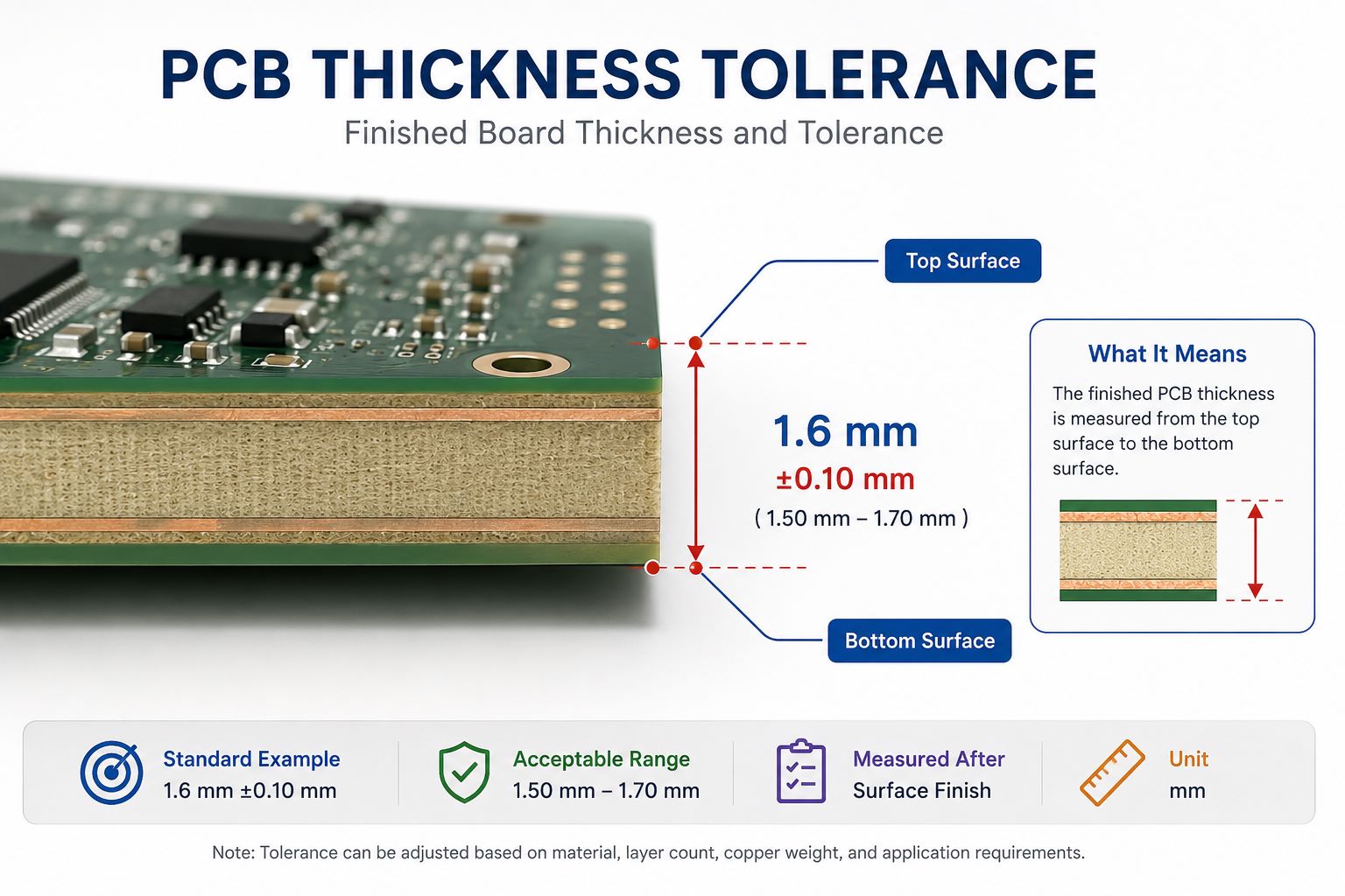
Thickness1.53 mm ±10%
FinishHASL Lead-Free
Solder MaskBlue
SilkscreenWhite
Hole Copper≄25 ÎŒm
AssemblySMT

For this project, the key manufacturing points were copper plating control, finished board thickness tolerance, hole copper reliability, lead-free HASL surface finish, and SMT readiness.

Our review process focused on three practical points:

  • Copper control: The outer copper started from 0.5 oz base copper and was plated to meet the 1 oz finished copper requirement.
  • Hole reliability: Minimum hole copper was controlled at ≄25 ÎŒm to support connection reliability.
  • Assembly readiness: The PCB was reviewed for SMT assembly after fabrication requirements were confirmed.

This case shows how a China printed circuit manufacturer for custom solutions should work. The manufacturer should not only fabricate the board, but also connect board parameters, plating control, surface finish, and assembly needs into one production plan.

What Industries Do Our Custom China Printed Circuit Solutions Serve?

Different industries have different PCB priorities. A medical PCB may need stable traceability and clean assembly. An automotive PCB may need stronger process control. A LED PCB may focus on thermal transfer. A communication board may require impedance and material stability.

EBest Circuit supports custom PCB and PCBA projects for many customer industries.

IndustryPCB Focus
AutomotiveReliability, Thermal
MedicalTraceability, Clean Assembly
AerospaceHigh Reliability
IndustrialRepeat Orders
LED LightingHeat Dissipation
Power ElectronicsHeavy Copper
RF CommunicationImpedance, RF Material
IoT SensorsCompact Design
Consumer ElectronicsCost + Speed

These industries show why “custom solutions” matter. A single standard PCB process cannot fit all product conditions.

EBest Circuit helps buyers select materials, structures, assembly processes, and test methods according to real application needs. This is important for products that require stable performance across prototype, pilot run, and mass production.

How Do We Provide Fast Quotes, MOQ, Lead Time, And Mass Production Support?

A clear quotation process helps buyers save time. A fast quote should not be a rough guess; it should be based on production-ready information.

For bare PCB quotation, please provide:

  • Gerber files
  • Drill files
  • Board quantity
  • Material type
  • Layer count
  • Board thickness
  • Copper thickness
  • Surface finish
  • Solder mask and silkscreen color
  • Impedance requirements, if any
  • Special tolerance or testing requirements

For PCBA quotation, please also provide:

  • BOM
  • Pick-and-place file
  • Assembly drawing
  • Component sourcing rules
  • Testing method
  • Packaging requirement
  • Approved substitute rules, if allowed

Our MOQ depends on PCB type, material, component sourcing, panel utilization, testing setup, and production process. Prototype and small-batch orders are accepted, while mass production pricing is calculated based on quantity, material usage, tooling, assembly time, component availability, and testing requirements.

For lead time, urgent PCB boards can be shipped within 24 hours when files, material, process, and capacity are suitable. SMT assembly lead time is typically 1–5 days after files, components, and production conditions are confirmed.

This quotation method gives customers a practical path from prototype to mass production. It also helps prevent price changes caused by missing files or unclear technical requirements.

What Import And Shipping Documents Do Overseas PCB Buyers Need?

For overseas PCB buyers, import and shipping documents are more practical than guessing whether every shipment is duty free. Tariff treatment can change based on product classification, destination country, product condition, origin rules, and local customs policy.

The U.S. HTS describes printed circuits under heading 8534 as circuits formed on an insulating base by a printing process, such as plating-up or etching. USTR also extended certain China Section 301 exclusions until November 10, 2026, but applicability depends on the exact product description and tariff classification.

EBest Circuit supports overseas buyers by preparing clear export and shipping documents.

Common documents include:

  • Commercial invoice
  • Packing list
  • Product description
  • Shipping mark
  • Delivery address information
  • Declared product details
  • Export coordination documents
  • Test report, when required
  • Material or compliance documents, when required

For U.S. importers, bare printed circuits may be classified differently from assembled PCBAs, flexible circuits, ceramic PCBs, or electronic modules. Buyers should confirm HS or HTS classification with their customs broker before shipment.

Our role is to provide accurate product information, commercial documents, packing details, and logistics coordination. The final customs classification and duty decision should be confirmed by the importer or customs broker.

FAQs About China Printed Circuit

This section answers common buyer questions about EBest Circuit, custom PCB production, PCBA capability, equipment, quality control, MOQ, lead time, and required files.

What is a China printed circuit manufacturer?
A China printed circuit manufacturer produces printed circuit boards in China for electronic products. A full-service manufacturer may also provide PCB assembly, component sourcing, testing, packaging, and export delivery.

Is EBest Circuit a China printed circuit manufacturer for custom solutions?
Yes. EBest Circuit (Best Technology) provides custom PCB fabrication and PCBA services, including FR4 PCB, multilayer PCB, HDI PCB, flexible PCB, rigid-flex PCB, metal core PCB, ceramic PCB, high-frequency PCB, SMT assembly, THT assembly, and mixed assembly.

What certifications does EBest Circuit have?
EBest Circuit supports quality systems and compliance requirements including ISO 9001:2015, ISO 13485:2016, IATF 16949, AS9100D, UL, REACH, and RoHS. Project inspection can also follow IPC-based standards such as IPC-A-600 and IPC-A-610 when required.

What is your monthly PCB capacity?
Our monthly PCB capability reaches about 260,000 square feet / 28,900 square meters. More than 1,000 different board designs can be completed monthly.

What SMT capability does EBest Circuit provide?
Our SMT capability includes 13.2M chips/day placement capacity, 01005 minimum SMD component, 0.25 mm minimum BGA pitch, SMT/THT/mixed assembly, and 1–5 days assembly lead time after files and materials are confirmed.

What equipment supports your PCB assembly process?
Our PCBA workflow can include solder paste printing, SPI, SMT placement, reflow soldering, AOI, X-ray inspection, THT assembly, wave soldering or manual soldering when required, functional testing, and final inspection.

Can EBest Circuit provide test reports or inspection records?
Yes. Depending on project requirements, we can provide electrical test records, impedance test data, first article inspection records, X-ray inspection images, functional test records, and outgoing inspection reports.

What files are needed for a PCB quote?
For bare PCB, please send Gerber files, drill files, quantity, material, copper thickness, board thickness, surface finish, solder mask color, and special requirements. For PCBA, please also send BOM, pick-and-place file, assembly drawing, and test requirements.

What is the MOQ for custom PCB or PCBA orders?
MOQ depends on board type, material, component package, assembly process, testing setup, and production planning. We support prototypes, small batches, and mass production.

How fast can EBest Circuit deliver PCB or PCBA orders?
Urgent PCB boards can be shipped within 24 hours when project conditions allow. SMT assembly lead time is usually 1–5 days after files, components, and production details are confirmed.

Can EBest Circuit support mass production after prototype approval?
Yes. We support prototype, small-batch, repeat order, and mass production. For mass production, we can help review manufacturability, panel design, testing method, component sourcing, and quality control requirements.

How can I start a custom PCB or PCBA project with EBest Circuit?
Send your Gerber files, BOM, assembly drawings, quantity, material requirements, and testing needs to sales@bestpcbs.com. Our team will review the files and provide quotation, lead time, and engineering feedback.

Overall, China printed circuit manufacturer for custom solutions means a PCB production partner that can prove its capability through process data, certifications, assembly control, quality inspection, case experience, and delivery support. This article explained how EBest Circuit supports custom PCB fabrication, SMT/THT assembly, material selection, process control, industry applications, quotation, MOQ, lead time, and overseas shipping documents.

EBest Circuit (Best Technology) combines over 20 years of PCB experience, 260,000 square feet monthly capacity, ISO/IATF/UL-related quality systems, IPC-based inspection support, 13.2M chips/day SMT capability, and one-stop PCB/PCBA service for global customers.

For custom PCB fabrication, printed circuit board assembly, prototype orders, or mass production support, pls feel free to contact EBest Circuit (Best Technology) at sales@bestpcbs.com.

You may also like

Circuit Board Markings: How to Read PCB Symbols & Codes

July 6th, 2026

Circuit board markings are the letters, numbers, symbols, polarity signs, and reference codes printed on a PCB to help identify components, assembly direction, test points, safety areas, and possible defects. This guide explains how to read PCB symbols and codes, including component markings, polarity labels, fuse markings, burn marks, water marks, and common PCB inspection questions.

If you are sourcing trusted PCB or quality-focused PCBA services, unclear markings can create real problems during assembly, repair, inspection, and quality control. A small missing polarity mark or unreadable reference designator may lead to wrong component placement, delayed debugging, failed testing, or costly rework.

What problems do customers often face when circuit board markings are unclear?

  • They cannot tell whether a mark is a label or a defect.
  • They confuse component codes such as R, C, D, Q, U, J, F, and TP.
  • They miss polarity marks and install parts in the wrong direction.
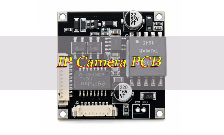
  • They struggle to judge burn marks, scorch marks, or water marks.
  • They receive boards with poor silkscreen readability.

A professional PCB and PCBA manufacturer helps prevent these issues before production starts.

  • We review silkscreen clarity before PCB fabrication.
  • We check reference designators against the BOM and assembly files.
  • We verify polarity marks for capacitors, diodes, ICs, and connectors.
  • We inspect abnormal burn marks, stains, and contamination.
  • We keep PCB markings consistent for assembly, testing, and repair.

EBest Circuit (Best Technology) is a professional PCB and PCBA manufacturer supporting custom PCB prototype, quick PCB fabrication, component sourcing, PCB SMT assembly, through-hole assembly, engineering review, and quality inspection. We help customers improve PCB layout readability, silkscreen accuracy, component identification, polarity control, and production reliability. For PCB or PCBA manufacturing support, contact us at sales@bestpcbs.com.

Circuit Board Markings

What Are Circuit Board Markings?

Circuit board markings are the visual information printed, etched, labeled, or laser-marked on a PCB. They help engineers, assemblers, inspectors, and repair technicians understand what each component, pad, connector, and test point is used for.

Most markings are printed on the silkscreen layer, but some may also appear as copper text, solder mask openings, adhesive labels, QR codes, barcodes, or laser marking.

Common circuit board markings include:

Marking TypeExamplePurpose
Reference designatorR1, C5, U2Identify components
Polarity mark+, -, dot, stripeShow direction
Test pointTP1, TP2Support electrical testing
Fuse markF1, F2Identify protection parts
Connector markJ1, CN1Show interface position
Revision codeREV A, V1.2Track design version

These markings are not decoration. They connect the physical PCB to the schematic, BOM, assembly drawing, test procedure, and repair documentation.

In short, circuit board markings are the map of a PCB. Without them, assembly and troubleshooting become slower, riskier, and more expensive.

Circuit Board Markings

How to Read Circuit Board Markings Step by Step

To read circuit board markings correctly, start with the obvious labels first, then move to smaller component codes and polarity symbols. This helps you avoid confusing normal PCB markings with damage or contamination.

A practical reading process is:

  • Find the board name, part number, or revision code.
  • Identify major components, connectors, and power input areas.
  • Read reference designators such as R, C, D, Q, U, J, F, and TP.
  • Check polarity markings before removing or installing components.
  • Compare the PCB markings with the schematic, BOM, and assembly drawing.
  • Inspect abnormal areas such as burn marks, water marks, or corrosion.
  • Confirm unclear markings with the manufacturer before repair or production.

For example, C12 usually means capacitor position 12. If the same footprint has a + mark, it may be a polarized capacitor and must be installed in the correct direction.
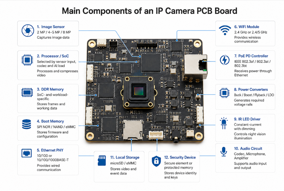
The safest approach is to read PCB markings together with technical files, not by visual guessing alone.

Common Printed Circuit Board Markings and What They Mean

Printed circuit board markings usually refer to the symbols and text printed on the silkscreen layer. These markings help identify components, orientation, test points, warnings, and manufacturing information.

Common printed circuit board markings include:

  • R: Resistor
  • C: Capacitor
  • D: Diode or LED
  • Q: Transistor or MOSFET
  • U or IC: Integrated circuit
  • J or CN: Connector
  • F: Fuse
  • TP: Test point
  • SW: Switch
  • L: Inductor
  • GND: Ground
  • VCC, VIN, 5V, 12V: Power net labels

Some PCBs also include UL marks, RoHS marks, date codes, lot codes, QR codes, or manufacturer identification. These are useful for traceability, compliance, and quality management.

For production, printed circuit board markings should be readable after soldering, cleaning, conformal coating, and final inspection. If the text is too small, too close to pads, or hidden under components, it may create assembly or repair problems.

Circuit Board Component Markings: R, C, D, Q, U, J, F, and TP

Circuit board component markings are usually reference designators. They do not always show the exact component value, but they tell you what type of component belongs in that position.

Here is a simple reference table:

MarkingComponent TypeExample
RResistorR10
CCapacitorC3
DDiode/LEDD5
QTransistor/MOSFETQ1
UIC/chipU2
J/CNConnectorJ1
FFuseF1
TPTest pointTP4

These component markings are important for SMT assembly, through-hole assembly, inspection, testing, and repair. During PCBA production, the assembler uses these reference designators together with the BOM and pick-and-place file.

If component markings are missing or inconsistent, technicians may need to trace the circuit manually. That can increase inspection time and raise the risk of assembly mistakes.

Clear circuit board component markings make the PCB easier to build, test, repair, and reproduce.

Circuit Board Markings

Circuit Board Capacitor Polarity Markings Explained

Circuit board capacitor polarity markings are important because polarized capacitors can fail if installed backward. Electrolytic capacitors and some tantalum capacitors are especially sensitive to polarity.

Common capacitor polarity markings include:

  • + mark for the positive pad
  • Shaded area or stripe for the negative side
  • Square pad or special pad shape
  • Silkscreen outline matching the capacitor body
  • Longer lead on through-hole capacitors as positive
  • Stripe on the capacitor body as negative

For PCBA production, capacitor polarity circuit board marking must match the BOM, assembly drawing, and component datasheet. If the PCB marking is unclear, the manufacturer should confirm orientation before mass production.

This is especially important for power supplies, LED drivers, motor control boards, battery systems, and industrial control PCBs.

In short, capacitor polarity markings help prevent reverse installation, overheating, leakage, and functional failure.

Polarity Markings on Circuit Boards: Positive, Negative, Diode, and IC Pin 1

Polarity markings on circuit boards show direction. They are critical for polarized components such as capacitors, diodes, LEDs, ICs, connectors, relays, batteries, and power input terminals.
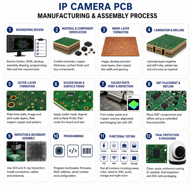
Typical polarity markings include:

  • + for positive voltage.
  • - for negative or ground.
  • Diode line mark for cathode direction.
  • Dot, notch, or bevel for IC pin 1.
  • Triangle or square pad for connector orientation.
  • Battery symbols for positive and negative terminals.

Positive marks on circuit board areas are useful, but they should never be interpreted alone. Always check the complete footprint, nearby labels, schematic, and component datasheet.

For manufacturers, polarity control is a key part of PCBA quality. A reversed diode, capacitor, IC, or connector can cause immediate board failure.

Good polarity marking reduces assembly errors, improves inspection speed, and protects the final product from avoidable electrical failure.

Circuit Board Fuse Markings and Other Safety Labels

Circuit board fuse markings help users identify protective components in power input, motor control, battery, industrial, automotive, and consumer electronic boards. Fuse markings usually appear as F1, F2, or similar labels.

Other safety-related PCB markings may include:

  • F: Fuse
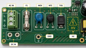
  • MOV: Surge protection component
  • NTC: Inrush current limiter
  • TVS: Transient voltage suppressor
  • GND: Ground
  • HV: High voltage warning
  • AC IN: AC power input
  • DC IN: DC power input

These labels help technicians locate protection circuits quickly during inspection or repair. They also help separate low-voltage, high-voltage, input, output, and ground areas.

For PCB manufacturing, safety labels should not be placed too close to pads, covered by large components, or removed during cleaning. If conformal coating is used, markings should remain visible where inspection is required.

Clear fuse markings and safety labels make the PCB safer to handle and easier to diagnose.

Circuit Board Markings

Are Burn Marks on Circuit Board the Same as Circuit Board Markings?

Burn marks on circuit board surfaces are not normal circuit board markings. They usually indicate overheating, overload, short circuit, poor soldering, component failure, contamination, or long-term electrical stress.

Common signs include:

  • Brown or black scorch marks
  • Darkened solder mask
  • Burnt smell around components
  • Discolored copper pads
  • Melted connector housing
  • Charred areas near power components

A circuit board burn mark should not be treated as a printed label. If burn marks appear near fuses, MOSFETs, resistors, capacitors, connectors, or power traces, the board should be inspected carefully before reuse.

Do scorch marks affect a circuit board? They can. Even if the board still works, heat damage may weaken the substrate, copper adhesion, solder joints, or nearby components.

Intentional PCB markings help identify parts. Burn marks are warning signs that the board may need testing, repair, or replacement.

Water Marks on Circuit Board: What They Indicate and When to Worry

Water marks on circuit board surfaces may come from moisture, cleaning residue, flux residue, leakage, condensation, poor storage, or environmental exposure. Some marks are only cosmetic, but others may affect electrical reliability.

Watch for these signs:

  • White residue near solder joints
  • Green corrosion around copper
  • Sticky or cloudy contamination
  • Rust on shields or connectors
  • Water stains near edge connectors
  • Intermittent electrical failure

Water marks are more serious when they appear on powered boards, high-voltage areas, fine-pitch ICs, connectors, or dense SMT layouts. Moisture can cause leakage current, corrosion, dendrite growth, short circuits, and long-term reliability problems.

In PCB and PCBA production, cleaning, drying, packaging, and storage conditions all matter. A professional manufacturer should control contamination and inspect abnormal stains before shipment.

Water marks should be evaluated separately from normal printed circuit board markings because they may indicate contamination or environmental damage.

FAQs About Circuit Board Markings

Circuit board markings help users read PCB symbols, codes, polarity signs, component labels, safety labels, and possible defect indicators. Below are common questions about PCB markings.

What do circuit board markings mean?
They identify components, polarity, connectors, test points, fuses, revision codes, safety labels, and sometimes compliance or traceability information.

How do I read circuit board markings?
Start with the board part number and revision code. Then read reference designators such as R, C, D, Q, U, J, F, and TP. Finally, check polarity and safety markings.

What does C mean on a circuit board?
C usually means capacitor. For example, C10 means capacitor position 10 on the PCB.

What does R mean on a circuit board?
R usually means resistor. The number after it identifies the resistor position.

What do polarity markings on circuit boards show?
They show positive, negative, cathode, anode, or pin 1 direction for components that must be installed in a specific orientation.

Are burn marks on circuit board normal?
No. Burn marks usually indicate overheating, overload, short circuit, poor soldering, or component failure.

Can water marks on a circuit board cause failure?
Yes. Moisture or residue can cause corrosion, leakage current, short circuits, or intermittent failure.

What are circuit board fuse markings?
Fuse markings usually appear as F1, F2, or similar labels. They identify protective fuse positions on the PCB.

What is the difference between PCB silkscreen and laser marking?
Silkscreen is printed on the PCB surface, while laser marking is engraved or marked by laser for traceability, barcodes, QR codes, or permanent identification.

Can EBest Circuit help improve PCB markings before production?
Yes. EBest Circuit (Best Technology) can review PCB files, silkscreen readability, polarity marks, component designators, assembly drawings, and PCBA manufacturability before production.

To summarize, circuit board markings are essential visual guides that help users understand PCB symbols, component codes, polarity direction, test points, safety labels, and possible damage signs. This article explained how to read PCB symbols and codes, including printed circuit board markings, component markings, capacitor polarity markings, fuse markings, burn marks, and water marks.

EBest Circuit (Best Technology) supports custom PCB fabrication and PCBA assembly with engineering review, clear silkscreen control, polarity checking, component placement verification, testing, and quality inspection. If you need reliable PCB or PCBA manufacturing support, pls feel free to contact us at sales@bestpcbs.com.
You may also like

Best Rigid PCB Manufacturer in China for Custom PCB Fabrication

July 3rd, 2026

Best rigid PCB manufacturer searches usually come from customers who need more than a basic board supplier. They want a manufacturer that can build rigid PCBs reliably, review Gerber files before production, control material and copper thickness, and support projects used in industrial controllers, automotive modules, communication systems, medical devices, LED products, and consumer electronics.

China has many PCB manufacturers, but not every supplier is suitable for custom rigid PCB projects. This article introduces the top 10 best rigid PCB manufacturers in China and explains why EBest Circuit (Best Technology) is a reliable choice for custom rigid PCB manufacturing. Need a rigid PCB quote? Pls feel free to send your Gerber files, drill files, material, copper thickness, board thickness, quantity, and special requirements to sales@bestpcbs.com.

Best Rigid PCB Manufacturer

Top 10 Best Rigid PCB Manufacturers in China

The list below is a practical reference for engineers, buyers, and project managers. It is not a financial ranking. It focuses on rigid PCB relevance, product capability, and project suitability.

No.ManufacturerMain Strength
1EBest Circuit (Best Technology)Custom rigid PCB, heavy copper, PCBA
2Kinwong ElectronicAutomotive, telecom, industrial PCB
3Shennan CircuitsPCB, substrate, assembly
4WUS Printed CircuitCommunication, automotive PCB
5Suntak PCBHigh multilayer, server PCB
6Fastprint Circuit TechPrototype, R&D boards
7Founder PCBCommunication, industrial PCB
8Bomin ElectronicsHDI, multilayer, rigid-flex
9Victory Giant TechnologyServer, automotive, industrial PCB
10Aoshikang TechnologyMultilayer, data center, electronics

EBest Circuit is suitable for customers who need more than a basic PCB supplier. It supports:

  • Single-sided and double-sided rigid PCB
  • Multilayer rigid PCB
  • HDI rigid PCB
  • High Tg rigid PCB
  • Heavy copper rigid PCB
  • Impedance control PCB
  • High-frequency PCB
  • PCB assembly and turnkey support

For customers, this means fewer supplier changes when a project moves from simple rigid PCB to complex multilayer, heavy copper, or assembled boards.

Best Rigid PCB Manufacturer

What Makes a Company One of the Best Rigid PCB Manufacturers in China?

A good rigid PCB manufacturer should not be judged only by price. Low cost may look attractive, but weak engineering review or poor process control can create expensive problems later.

A reliable rigid PCB manufacturer should have three strengths.

1. Real manufacturing capability

The supplier should handle different board structures, not only standard FR4 boards.

Key capabilities to check:

  • Layer count
  • Board thickness
  • Copper thickness
  • Line width and spacing
  • Drilling capability
  • Surface finish
  • Impedance control

2. Engineering review before production

A good manufacturer should check your files before fabrication. This helps catch risks early, such as tight spacing, difficult hole design, unsuitable copper thickness, or unclear stack-up notes.

3. Stable quality control

Rigid PCB quality depends on drilling, plating, imaging, etching, solder mask, surface finish, and electrical testing. The best manufacturer should control these steps with clear inspection standards.

Customer takeaway:
The best rigid PCB manufacturer is not the one that simply says “we can make it.” It is the one that can tell you how the board will be made, what risks exist, and how those risks will be controlled.

Who Is EBest Circuit (Best Technology)?

EBest Circuit (Best Technology) is a PCB manufacturer in China. The company provides rigid PCB, flexible PCB, rigid-flex PCB, metal core PCB, ceramic PCB, HDI PCB, high-frequency PCB, heavy copper PCB, and PCB assembly services.

For rigid PCB projects, EBest Circuit is suitable for customers who need:

  • Custom board structures
  • Engineering review
  • Material selection support
  • Heavy copper capability
  • Multilayer manufacturing
  • Prototype-to-production support
  • PCB fabrication plus assembly

EBest Circuit is not only a bare board supplier. It can also help customers review production risks before the board enters fabrication.

That matters because many PCB problems begin before production. Common risks include unclear files, poor hole design, wrong material selection, insufficient spacing, unrealistic copper requirements, or missing assembly notes.
What Rigid PCB Manufacturing Capabilities Does EBest Circuit Offer?

EBest Circuit supports both standard and complex rigid PCB projects.

CapabilityEBest Circuit
Layers1–50 regular
Special layersEngineering review
Board thickness0.4–6.0mm regular
Special thickness0.15–10mm review
Inner copperUp to 6oz regular
Outer copperUp to 10oz regular
Special outer copperUp to 28oz review
Mechanical hole0.15–6.5mm
Laser drilling0.10mm regular
Special laser via0.070mm review

These capabilities allow EBest Circuit to support more than common FR4 boards. It can also review rigid PCB projects involving heavy copper, thick boards, HDI structures, small vias, controlled impedance, and special surface finishes.

Best-fit project types

  • Industrial control PCB
  • Automotive electronics PCB
  • Power electronics PCB
  • Communication equipment PCB
  • High-current rigid PCB
  • Multilayer FR4 PCB
  • High Tg rigid PCB
  • Impedance control PCB

Customer takeaway:
If your rigid PCB has special thickness, high copper, many layers, or controlled impedance, EBest Circuit can review the project before production instead of giving a blind quote.

How Does EBest Circuit Review Your Rigid PCB Files Before Production?

File review helps prevent production problems before they happen. This is especially important for thick boards, heavy copper boards, multilayer PCBs, and impedance-controlled designs.

Files to send

For a faster quotation, prepare:

  • Gerber files
  • Drill files
  • Stack-up drawing
  • Board thickness
  • Copper thickness
  • Material requirement
  • Surface finish
  • Quantity
  • Special notes
  • BOM and pick-and-place files, if assembly is needed

What EBest Circuit checks

Check ItemMain Purpose
Line / spacingEtching safety
Copper weightCurrent and process fit
Hole designPlating reliability
Stack-upThickness and impedance
Solder maskPad protection
Surface finishAssembly fit
Tolerance notesProduction control

This review is useful because one small design choice can affect several manufacturing steps.

For example, 10oz copper needs more spacing than standard copper. A very thick board needs careful drilling and plating review. An impedance-controlled board needs the stack-up, dielectric thickness, and trace width to match the target value.

Customer takeaway:
A good file review reduces redesign, production delay, and unexpected cost.

What Materials Can EBest Circuit Use for Rigid PCB Manufacturing?

Material choice affects heat resistance, electrical performance, soldering reliability, and product life.

EBest Circuit supports different material options for different applications.

MaterialSuitable Use
Standard FR4General electronics
Middle Tg FR4Better heat resistance
High Tg FR4Industrial and automotive
High CTI materialInsulation reliability
High-speed materialFast signal transmission
Rogers materialRF and microwave
PTFE materialLow-loss high frequency

For many standard products, FR4 is enough. For high-temperature or demanding operating environments, high Tg FR4 is usually a safer choice. For RF or high-speed signal products, Rogers, PTFE, or low-loss materials may be needed.

Customer takeaway:
The best material is not always the most expensive one. The right choice should match the board’s temperature, signal, insulation, mechanical, and cost requirements.

How Does EBest Circuit Control Rigid PCB Quality?

Rigid PCB quality is not created by one final inspection. It is controlled step by step during the whole manufacturing process.
Main quality control points

  • Material inspection
  • Inner layer inspection
  • Lamination control
  • Drilling inspection
  • Copper plating control
  • Outer layer inspection
  • Solder mask inspection
  • Surface finish inspection
  • Electrical test
  • Final inspection

Key tests and inspections

ProcessPurpose
AOIPattern check
Electrical testOpen / short check
Impedance testSignal control
Hole inspectionPlating reliability
Surface finish checkSolderability
Final inspectionOverall quality

For heavy copper, thick boards, and multilayer rigid PCBs, hole plating and lamination control are especially important. These details affect electrical continuity, mechanical strength, and long-term reliability.

Customer takeaway:
Good quality control is not only about finding defects. It is about preventing defects before the board reaches the customer.

Best Rigid PCB Manufacturer

Why Is EBest Circuit Suitable for Complex Rigid PCB Projects?

Some rigid PCBs are simple. Others combine several difficult requirements in one board.

EBest Circuit is suitable for complex rigid PCB projects because it can review and process multiple requirements together.

Complex requirements EBest Circuit can support

  • High layer count
  • Thick board structure
  • Heavy copper
  • Small holes
  • Laser vias
  • High aspect ratio holes
  • Controlled impedance
  • Back drilling
  • Resin plugged vias
  • Gold fingers
  • High Tg materials
  • High-frequency materials

A complex rigid PCB usually has more than one challenge.

For example:

Heavy copper PCB
Needs wider spacing, etching compensation, good solder mask coverage, and strong plating control.

High-speed rigid PCB
Needs stack-up control, impedance calculation, low-loss material, and sometimes back drilling.

Industrial control PCB
Needs reliable FR4 material, stable hole plating, suitable copper thickness, and strong electrical testing.

Customer takeaway:
For complex boards, engineering review is not optional. It is part of reliable manufacturing.

How Does EBest Circuit Support Customers Beyond Rigid PCB Manufacturing?

Many customers start with rigid PCB. Later, the same project may need another board type or assembly service.

EBest Circuit can support related PCB solutions, which helps customers reduce supplier switching.

SolutionWhen It Helps
Flexible PCBSmall and light devices
Rigid-flex PCBSpace-saving design
Metal core PCBHeat dissipation
Ceramic PCBHigh thermal reliability
High-frequency PCBRF and microwave
PCB assemblyFinished modules

This is useful for product families. One product may use rigid PCB for the controller, metal core PCB for LED power, and rigid-flex PCB for compact connection.

Customer takeaway:
Working with one capable supplier can make communication easier and reduce sourcing work.

Best Rigid PCB Manufacturer

Why Choose EBest Circuit as Your Rigid PCB Manufacturer in China?

EBest Circuit is a practical choice for customers who need custom rigid PCB manufacturing, engineering support, and flexible production capability.

Why customers choose EBest Circuit

  • Custom rigid PCB support
  • Heavy copper manufacturing
  • Multilayer PCB capability
  • High Tg material options
  • Controlled impedance support
  • File review before production
  • PCB fabrication and assembly
  • Support for special PCB types

Best-fit customers

EBest Circuit is suitable for customers who:

  • Need more than standard FR4 PCB
  • Have complex board requirements
  • Need engineering feedback before production
  • Want PCB fabrication and assembly support
  • Work with industrial, automotive, power, communication, or high-reliability products

Ready to quote your rigid PCB? Pls feel free to send your project files to sales@bestpcbs.com. For faster response, include Gerber files, drill files, material, copper thickness, board thickness, surface finish, quantity, and any special notes.

Case Study: How EBest Circuit Supports a Custom Rigid PCB Project

A customer needed a 16-layer rigid PCB for a high-current industrial control application. This was not a standard multilayer FR4 board. The project combined thick board construction, heavy copper, multilayer lamination, and reliable hole plating.
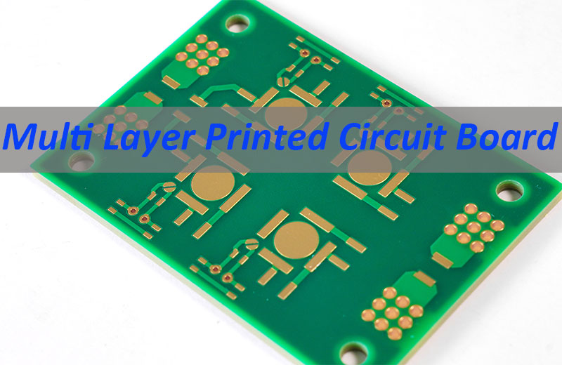
Project goal

Build a rigid PCB that could support:

  • High current
  • Stable electrical connection
  • Strong plated holes
  • Reliable long-term use
  • Industrial operating conditions

Main challenges

ChallengeRisk
16 layersLayer alignment
11.382mm thicknessDrilling difficulty
10oz copperEtching and spacing
35ÎŒm hole copperPlating reliability
ENIG finishAssembly surface

How EBest Circuit supported the project

Before production, EBest Circuit reviewed the customer’s Gerber files, stack-up, copper thickness, hole design, solder mask design, surface finish requirement, and tolerance notes.

The engineering team focused on:

  • Line width and spacing for 10oz copper
  • Hole design for a very thick board
  • Copper-to-copper clearance
  • Layer stack-up balance
  • Solder mask opening and coverage
  • ENIG finish suitability
  • Plated hole reliability

Production focus

1. Lamination stability

  • A 16-layer board with heavy copper needs stable lamination. The structure must maintain bonding, thickness control, and layer registration.
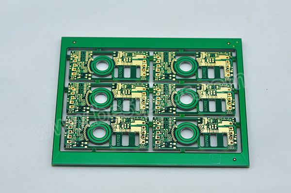
2. Drilling quality

  • The board thickness was 11.382mm ±10%, so drilling quality was critical. Poor hole walls could affect copper plating and long-term reliability.

3. Heavy copper processing

  • Both inner and outer copper were 10oz. This required careful process control for etching, spacing, solder mask coverage, and final appearance.

Final result

This project showed EBest Circuit’s ability to support a complex rigid PCB with heavy copper, thick board construction, multilayer structure, and controlled hole plating.

For industrial control, power electronics, battery systems, and high-current equipment, this kind of engineering support is valuable because risks are reviewed before production and controlled during fabrication.

Key PCB specifications

ItemSpecification
PCB type16-layer rigid PCB
MaterialFR4 TG170
Dk4.8
Thickness11.382mm ±10%
Copper10oz inner / outer
Hole copper35ÎŒm
FinishENIG, Au 1ÎŒin
Mask / silkscreenGreen / white
FocusHeavy copper, thick board, plating

Have a similar rigid PCB project? Pls feel free to send your board files and requirements to sales@bestpcbs.com. EBest Circuit can review the design and confirm whether the stack-up, copper thickness, hole structure, and surface finish are suitable for production.

FAQs About Best Rigid PCB Manufacturer

What is the best rigid PCB manufacturer in China?

The best rigid PCB manufacturer should match your project needs. For custom rigid PCB, heavy copper PCB, multilayer PCB, HDI PCB, and PCBA support, EBest Circuit is a reliable choice in China.

How do I choose a rigid PCB manufacturer?

Check material support, layer capability, copper thickness, drilling ability, surface finish, impedance control, quality inspection, and engineering support.

Is EBest Circuit a rigid PCB manufacturer?

Yes. EBest Circuit, also known as Best Technology, manufactures rigid PCBs, including single-sided, double-sided, multilayer, HDI, high Tg, heavy copper, high-frequency, and impedance-controlled boards.

Can EBest Circuit manufacture heavy copper rigid PCBs?

Yes. EBest Circuit can support heavy copper rigid PCB projects. Regular outer copper capability can reach up to 10oz, and special projects can be reviewed up to 28oz.

Can EBest Circuit support multilayer rigid PCBs?

Yes. EBest Circuit supports regular rigid PCB production from 1 to 50 layers. Higher-layer projects can be reviewed by the engineering team.

What files are needed for a rigid PCB quote?

Gerber files, drill files, board thickness, copper thickness, material, surface finish, solder mask color, quantity, and special notes are usually needed. For assembly, BOM and pick-and-place files are also required.

What is the difference between rigid PCB and rigid-flex PCB?

A rigid PCB keeps a fixed shape and is used in stable electronic assemblies. A rigid-flex PCB combines rigid and flexible sections for compact designs or products that need fewer connectors.

Can EBest Circuit provide PCB assembly?

Yes. EBest Circuit can provide PCB assembly support, including PCB fabrication, component sourcing, SMT assembly, and testing support.

To summarize, the best rigid PCB manufacturer should do more than fabricate boards. It should help customers review design risks, choose suitable materials, control key processes, and deliver stable quality. EBest Circuit (Best Technology) is a reliable rigid PCB manufacturer in China for customers who need standard rigid PCB, multilayer PCB, heavy copper PCB, high Tg PCB, high-frequency PCB, impedance control PCB, and PCBA support. For customers comparing rigid PCB suppliers or looking for the best rigid-flex PCB manufacturers for aerospace applications, EBest Circuit can also support projects that require engineering review, stable materials, and high-reliability manufacturing. If you are looking for a rigid PCB manufacturer in China, you can send your project files to sales@bestpcbs.com for review and quotation.

You may also like

Large PCB Manufacturer in China, Custom Solutions & Free DFM

July 2nd, 2026

A large PCB is a circuit board with dimensions beyond common production or assembly handling ranges. It is used in industrial control, LED display, power electronics, telecom equipment, testing systems and large electronic modules.

Compared with a standard board, it requires better flatness control, copper balance, drilling accuracy, material stability and assembly support. For buyers, the real challenge is not size alone. The board must stay reliable during fabrication, assembly, testing, shipment and final installation.

Are you worried about these problems in large PCB projects?

  • Design risk: Unbalanced copper, weak support points, unsuitable thickness or poor connector layout may cause bending, cracking or installation stress.
  • Production risk: Oversized panels may face uneven plating, solder mask defects, dimensional deviation, routing stress and longer production cycles.
  • Assembly risk: Long boards may bend during printing, placement, reflow, inspection or final testing without stable fixture support.

As a PCB manufacturer with 20+ years of experience, EBest Circuit helps global OEM factories, engineering companies and industrial equipment brands turn complex large PCB designs into stable production. Below are our solutions to these above challenges of large PCB board:

  • Free DFM review before production: We review board size, stack-up, copper weight, material, drill design, panel direction and connector layout to reduce design mistakes before fabrication starts.
  • Controlled large PCB manufacturing: We focus on copper balance, plating uniformity, solder mask coverage, dimensional tolerance and flatness control to improve production stability and batch consistency.
  • Reliable assembly and testing support: We check BOM, CPL, stencil design, component height, fixture needs and testing requirements to reduce soldering defects, board deformation and rework risk.

Welcome to contact us if you have any request for large PCB manufacturing and assembly: sales@bestpcbs.com.

Large PCB, https://www.bestpcbs.com/blog/2026/07/large-pcb/

What Is a Large PCB Board?

A large PCB board is a printed circuit board with a size larger than normal production or assembly handling capability. It may also be called an oversized PCB, large format PCB or large size PCB board.

This term refers to board dimensions, not order quantity. A project can be one sample and still require special production control if the outline is long, wide, thick or hard to handle.

Reliability is the main concern. Bigger boards are more sensitive to material expansion, copper imbalance, bending force and shipping damage. For this reason, both electrical design and mechanical support should be reviewed before production.

What Applications Commonly Use Large Size PCB Boards?

Large size PCB boards are used when one continuous circuit area can reduce cables, connectors and mechanical complexity. They are common in products with wide layout space, long current paths or large installation structures.

Common large PCB applications include:

  • Industrial control equipment: motor drives, power control modules, control cabinets and automation systems.
  • LED display systems: display panels, long lighting modules and outdoor signage boards.
  • Power electronics: UPS systems, inverters, charging equipment and high-current controllers.
  • Telecom equipment: backplanes, antenna control modules and communication power boards.
  • Medical equipment: diagnostic machines, imaging platforms and large control modules.
  • Testing systems: inspection fixtures, laboratory instruments and burn-in platforms.

In these projects, stable size, strong support and controlled assembly matter more than simply making a bigger circuit board.

What Size Range Can Large PCB Fabrication Support?

Large PCB fabrication capability depends on equipment size, material type, layer count, copper weight, board thickness and tolerance level. A two-layer oversized board is usually easier to manufacture than a large multilayer board with heavy copper and tight registration.

ItemTypical Range
Standard panel457 × 610 mm
Oversized range500 × 600 mm to 600 × 1200 mm
Board thickness1.6 mm to 4.0 mm
Heavy copper3 oz to 10 oz+
Layer count1 to 20+ layers
Line toleranceProject-based review
Bow/twist target≀0.75% for many SMT boards
Testing100% electrical test recommended

Maximum size PCB fabrication must be confirmed with Gerber files. Slots, cutouts, copper coverage, drill density, surface finish and assembly process may reduce the practical size limit.

What Are the Main Challenges in Large PCB Manufacturing?

Large PCB manufacturing is more difficult because size increases stress, handling difficulty and process variation.

  • Board warpage: Long or wide boards may bend during lamination, curing, reflow or storage if copper balance and thickness are not well controlled.
  • Dimensional deviation: Oversized panels are more affected by material expansion, routing stress and drilling position shift.
  • Uneven copper plating: A larger board area can make current distribution harder to control, especially for heavy copper or dense hole designs.
  • Solder mask defects: Large surface areas may increase the risk of uneven coating, poor edge coverage, misalignment or weak adhesion.
  • Hole wall reliability: Thick or large boards require stable drilling, desmear and plating control to keep plated through holes reliable.
  • Handling damage: Large boards are easier to scratch, bend or damage at corners during production, inspection, packing and shipment.
  • Assembly deformation: If the board is long, thin or heavy, it may bend during SMT printing, component placement and reflow.

The main goal is to control flatness, copper balance, hole quality and safe handling from the beginning of production.

How to Design a Large PCB for Stable Performance?

Step 1: Confirm board size and installation method.
Start with the final product structure. Check the available installation space, fixing method, screw hole position, connector direction and mechanical support. A large PCB should be designed for the real enclosure, not only for the circuit layout.

Step 2: Select suitable thickness and material.
A long or wide board usually needs stronger rigidity. Common thickness choices include 1.6 mm, 2.0 mm, 2.4 mm, 3.2 mm and 4.0 mm, depending on size, copper weight and component loading. FR-4 is suitable for general use, while high Tg FR-4 or metal base material may be better for heat or power applications.

Step 3: Balance copper distribution.
Avoid placing heavy copper only on one side or one local area. Uneven copper can pull the board during lamination and heat processing. For multilayer designs, copper planes should be as balanced as possible between layers.

Step 4: Design high-current areas carefully.
For power circuits, use proper trace width, copper weight, via size and spacing. Heavy copper can improve current carrying capacity, but it also requires larger spacing and better etching control. Heat flow should be reviewed together with the copper layout.

Step 5: Add mechanical support.
Use mounting holes, stiffeners, support ribs or fixing points when the board is long or carries heavy components. Terminals, transformers, relays and connectors should be placed near supported areas when possible.

Step 6: Reserve assembly and handling space.
Leave enough board edge clearance for SMT conveyors, fixtures, testing tools and packaging. If the board is too close to its outline limit, assembly handling may become unstable.

Step 7: Review files before prototype production.
Before large PCB prototype production, check Gerber files, drill files, stack-up, copper weight, solder mask, BOM, CPL, testing method and packaging needs. This helps reduce rework before mass production.

large PCB design, https://www.bestpcbs.com/blog/2026/07/large-pcb/

What Thickness Is Suitable for a Large Size PCB Board?

Thickness should match board size, component weight, copper weight and mounting method. A thin oversized board may bend during SMT or transportation, while an overly thick board may increase cost and drilling difficulty.

ApplicationCommon Thickness
Control board1.6 mm
Industrial board2.0 mm to 2.4 mm
Heavy component board2.4 mm to 3.2 mm
Power board2.0 mm to 3.2 mm
Heavy copper board2.4 mm to 4.0 mm
BackplaneProject-based design

For large custom PCB panel thickness, the best choice should be reviewed with outline size, copper weight and mounting structure. A balanced design is usually more reliable than simply choosing the thickest board.

How Does Copper Thickness Affect Large PCB Fabrication?

Copper thickness affects current capacity, temperature rise, etching accuracy, solder mask coverage and final flatness. For power equipment, heavy copper can improve current carrying ability and heat spreading.

Copper WeightCommon Use
1 ozSignal and control circuits
2 ozMedium current circuits
3 ozEntry-level heavy copper
4 oz to 6 ozIndustrial power boards
8 oz to 10 oz+High-current custom boards

However, thicker copper also makes production harder. It requires wider spacing, better etching compensation and stricter plating control. If copper is concentrated in one area, the board may bend during lamination or reflow.

Heavy copper large PCB fabrication should always review copper balance, minimum spacing, hole copper and heat requirements together.

What Materials Are Commonly Used for Large Format PCB Boards?

Large format PCB boards commonly use FR-4, high Tg FR-4, aluminum base, copper base or RF laminates. Material selection should match working temperature, current load, mechanical support and product environment.

MaterialSuitable Use
FR-4General industrial boards
High Tg FR-4Higher heat resistance
Aluminum baseLED and heat dissipation
Copper baseHigh-power heat design
Rogers materialRF and high-frequency circuits
Heavy copper FR-4Power electronics
Halogen-free FR-4Environmental compliance

FR-4 is the most common material because it offers balanced cost and performance. High Tg material is better for multilayer structures or products exposed to repeated heat.

For LED, inverter or high-power designs, metal base materials may help with heat transfer. The final material should be selected by working environment, not only by board size.

What Should Be Checked Before Large PCB Prototype Production?

Before large PCB prototype production, the design should be checked for fabrication, assembly, testing and packaging. This step helps avoid expensive rework before batch production.

Before production, review:

  • Gerber files: outline, copper layers, drill data, slots, solder mask and silkscreen.
  • Stack-up: layer count, dielectric thickness, copper weight and material grade.
  • Board outline: size, cutouts, routing path and fixture space.
  • Copper balance: large copper areas, heavy copper zones and plane symmetry.
  • Hole design: drill size, annular ring, plated holes and aspect ratio.
  • Assembly data: BOM, CPL, polarity, connector direction and component height.
  • Testing plan: electrical test, AOI, functional test and inspection standard.
  • Packaging plan: board separation, corner protection and moisture control.

A complete review improves first-pass success and makes later production more predictable.

How Is a Large PCB Manufactured Step by Step?

Step 1: Engineering review.
Production starts with Gerber, drill file and stack-up review. The factory checks board size, material, copper weight, thickness, hole design, spacing, surface finish, tolerance and assembly requirements. If warpage or copper balance risk is found, DFM feedback is given before production.

Step 2: Material preparation.
The laminate, copper foil and prepreg are prepared according to the confirmed specification. For oversized boards, material thickness, Tg, copper weight and cutting direction must be controlled to reduce stress during later processes.

Step 3: Inner layer production.
For multilayer boards, inner layers are imaged, etched and inspected first. AOI is used to check opens, shorts, line width and spacing before lamination. Any inner layer defect should be removed before the board is pressed.

Step 4: Lamination.
Inner layers, prepreg and copper foil are pressed together under controlled temperature, pressure and time. Large boards are more sensitive to heat and pressure changes, so lamination stability directly affects flatness and dimensional accuracy.

Step 5: Drilling, desmear and copper plating.
After lamination, holes and slots are drilled. The hole walls are cleaned by desmear, then plated with copper to create electrical connection between layers. For thick or heavy copper boards, hole wall quality must be checked carefully.

Step 6: Outer layer imaging and etching.
The outer circuit pattern is transferred and etched. Heavy copper designs need proper etching compensation because thicker copper is harder to control. Line width, spacing and copper residue should be inspected after etching.

Step 7: Solder mask and surface finish.
Solder mask is applied, exposed and cured. The process must control coverage, adhesion and alignment. Then the selected surface finish, such as HASL, ENIG or OSP, is applied according to assembly and storage requirements.

Step 8: Routing, testing and packaging.
The board outline, slots and cutouts are routed. After that, the board goes through AOI, electrical testing, dimensional inspection, flatness review and visual inspection. Finally, reinforced packaging is used to reduce bending, scratches and corner damage during shipment.

large PCB manufacturing process, https://www.bestpcbs.com/blog/2026/07/large-pcb/

What Is the Difference Between Standard PCB and Large PCB Fabrication?

The difference is not only size. Standard boards mainly focus on circuit accuracy, drilling quality, solder mask and electrical testing. Large PCB fabrication must also control mechanical stress, board support, flatness and packaging safety.

ItemStandard PCBOversized PCB
Size riskLowHigh
Warpage riskLowerHigher
Copper balanceImportantCritical
Plating controlEasierMore difficult
Routing stressLowerHigher
SMT handlingStandard supportFixture may be used
PackagingNormal cartonReinforced protection
Cost driverLayers and quantitySize, yield and handling

A standard board may pass with normal handling, but an oversized board can fail because of bending or deformation. That is why factory experience and engineering review matter.

How Does Large Format PCB Assembly Work?

Step 1: Assembly file review.
The assembly team checks BOM, CPL, Gerber files, stencil design, component height, polarity, connector direction and testing requirements. This review confirms whether the board can pass printing, placement, reflow and inspection smoothly.

Step 2: Fixture and support planning.
Large format PCB assembly often needs extra support under the board. If the board is long, thin or heavy, fixtures may be prepared for solder paste printing, SMT placement, reflow and testing.

Step 3: Solder paste printing.
The board must stay flat during stencil printing. If the board bends, solder paste thickness may become uneven and cause bridging, insufficient solder or open joints.

Step 4: SMT component placement.
Components are placed according to the CPL file. Placement accuracy must remain stable across the full board area. Heavy components and tall connectors should be reviewed for handling and support.

Step 5: Reflow soldering.
The assembled board passes through a controlled reflow profile. Heat rise, peak temperature and cooling rate should be suitable for the board size, material and component mix. Stable support helps reduce bending during reflow.

Step 6: Through-hole and selective soldering.
If the design includes connectors, terminals or power components, through-hole soldering or selective soldering may be used after SMT. These areas should be checked for solder filling, wetting and mechanical strength.

Step 7: Inspection and functional testing.
AOI checks solder joints, polarity, missing parts and alignment. X-ray inspection may be used for hidden joints such as BGA or power packages. Functional testing verifies whether the assembled board works as required.

Step 8: Final cleaning and packaging.
After inspection, the board is cleaned if required and packed with proper support. Oversized PCB assembly services should include packaging protection to reduce bending and damage during transport.

How Do We Ensure Quality in Large PCB Manufacturing?

  • DFM review before production: We review board size, stack-up, copper balance, material, hole design, surface finish, testing needs and assembly risk before fabrication starts.
  • Material inspection: We check material type, thickness, Tg, copper weight and laminate condition to make sure the board matches the confirmed specification.
  • Lamination control: We control pressure, temperature and time to reduce internal stress, layer shift and warpage.
  • Drilling inspection: We check hole position, drill quality, burrs, slot accuracy and hole wall condition before plating.
  • Copper plating control: We inspect copper thickness, hole copper and plating uniformity, especially for heavy copper and high-current boards.
  • Solder mask inspection: We check solder mask alignment, coverage, adhesion, exposure quality and clearance around pads.
  • Dimensional inspection: We measure outline size, slots, cutouts, hole position and flatness according to project requirements.
  • Electrical testing: We use electrical testing to check opens and shorts before shipment.
  • Assembly quality control: For PCBA orders, we check solder paste printing, component placement, solder joints, connector strength and functional performance.
  • Packaging protection: We use board separation, corner protection, moisture control and reinforced packing to reduce bending and transport damage.

Our quality control focuses on prevention, not only final inspection. This helps large PCB boards stay stable from prototype to batch production.

large PCB manufacturing quality control, https://www.bestpcbs.com/blog/2026/07/large-pcb/

Case Study: Heavy Copper Oversized PCB for Industrial Power Equipment

Project Background
A customer needed an oversized heavy copper board for industrial power equipment. The product worked in a high-current environment and required stable power transmission, good heat spreading and strong mechanical support. The board also included terminal blocks and heavy components, so bending and solder joint stress were major concerns.

Customer Requirements
The customer required a large board outline, heavy copper areas, reliable plated through holes and stable assembly performance. The board had to support high current, reduce local heat rise and remain flat during production and reflow. The customer also needed a prototype that could move smoothly into batch production after validation.

Our Solution
EBest PCB reviewed the stack-up, copper balance, board thickness, spacing, hole copper and terminal layout before production. We found that some power zones had much higher copper coverage than other areas, which could increase deformation risk. Therefore, we adjusted the DFM suggestions, strengthened plating control, checked solder mask clearance and prepared reinforced handling during assembly.

Final Results
The finished board achieved stable current carrying capacity, improved heat distribution and better mechanical reliability. The sample passed customer validation and moved to batch production. This project showed that heavy copper large PCB fabrication should combine electrical design, heat control, flatness management and assembly support from the start.

What Large PCB Manufacturing Services Can EBest PCB Provide?

EBest PCB provides one-stop support for large PCB projects, from engineering review to finished PCB assembly. This helps customers reduce supplier communication, shorten project transfer time and control production risk.

  • PCB design review: We review board size, stack-up, copper balance, material, drill design and assembly risk before production.
  • Large PCB prototype: We support sample production for oversized PCB, heavy copper PCB, multilayer PCB and special material boards.
  • Mass production: We support batch production with a monthly capability of 260,000 square feet / 28,900 square meters.
  • Component sourcing: We help prepare components based on customer BOM requirements for PCBA orders.
  • PCB assembly: We provide SMT assembly, through-hole assembly, connector soldering, functional testing and final inspection.
  • Expedited service: For suitable urgent boards, shipment can be supported within 24 hours after production details are confirmed.

Our product capability covers FR4 PCB, multilayer PCB, metal core PCB, ceramic PCB, flexible PCB, rigid-flex PCB, high frequency PCB, heavy copper PCB, HDI PCB, high Tg PCB and impedance control PCB.

Why Choose EBest PCB as Large PCB Manufacturer in China?

Choosing EBest PCB helps customers reduce design risk, save communication time and move from prototype to production with stronger control.

  • Lower project risk: With 20+ years of PCB experience, our team can review large board risks before production, including warpage, copper balance, thickness, hole design and assembly handling.
  • Faster project transfer: PCB design review, prototype, mass production, component sourcing and PCB assembly can be handled through one supplier, reducing repeated communication between different vendors.
  • Stronger production support: With monthly capability of 260,000 square feet / 28,900 square meters, we can support both sample verification and batch orders.
  • More material choices: Customers can choose FR4, high Tg FR4, metal core, ceramic, flexible, rigid-flex, high frequency and heavy copper structures according to project needs.
  • Better compliance support: Certifications including IATF 16949, ISO 9001:2015, ISO 13485:2016, AS9100D, REACH, RoHS and UL help support automotive, medical, aerospace, industrial and general electronics projects.
  • Clearer delivery path: Expedited service is available for suitable urgent boards, helping customers handle tight project schedules.

For buyers, the value is simple: one China source factory, fewer project delays, clearer engineering support and more stable production control.

FAQs About Large PCB Boards

Q1: What files should I send for a large PCB quote?
A1: Please send Gerber files, drill files, board thickness, copper weight, material, surface finish, quantity and delivery request. For PCBA orders, also send BOM, CPL and testing requirements. Complete files help shorten quotation time and reduce production misunderstanding.

Q2: Can EBest PCB help review my design before production?
A2: Yes. EBest PCB can review board size, stack-up, copper balance, hole design, spacing, material and assembly risk before production. This helps customers find manufacturability problems before they become prototype or batch defects.

Q3: Can I start with samples before mass production?
A3: Yes. You can start with large PCB prototype production to verify size, flatness, copper performance, soldering and function. After sample approval, the project can move to batch production with confirmed process settings.

Q4: Can EBest PCB source components for PCBA orders?
A4: Yes. EBest PCB supports component sourcing based on customer BOM requirements. This helps customers reduce purchasing workload and keep PCB fabrication, component preparation and assembly in one project flow.

Q5: How fast can urgent boards be delivered?
A5: For suitable urgent boards, EBest PCB can support expedited service, and some boards can be shipped within 24 hours after all files, materials and production details are confirmed. Actual timing depends on board structure and process difficulty.

Q6: What certifications does EBest PCB have?
A6: EBest PCB is supported by IATF 16949, ISO 9001:2015, ISO 13485:2016, AS9100D, REACH, RoHS and UL. These certifications help customers meet project requirements in automotive, medical, aerospace, industrial and electronic products.

Q7: What PCB types can EBest PCB manufacture?
A7: EBest PCB can manufacture FR4 PCB, multilayer PCB, metal core PCB, ceramic PCB, flexible PCB, rigid-flex PCB, high frequency PCB, heavy copper PCB, HDI PCB, high Tg PCB and impedance control PCB.

Q8: Is EBest PCB a factory or a trading company?
A8: EBest PCB is positioned as a China source factory for custom PCB and PCBA solutions. Customers can work with one team for design review, prototype, mass production, component sourcing and PCB assembly.

Q9: Can EBest PCB support regulated industry projects?
A9: Yes. With certifications such as IATF 16949, ISO 13485:2016 and AS9100D, EBest PCB can support projects in automotive, medical, aerospace and industrial fields. Final requirements should be confirmed by customer drawings and specifications.

Q10: How can I reduce risk before placing a batch order?
A10: Start with complete files, request design review, build samples, test the board and confirm assembly performance before mass production. This process is safer for oversized boards because size, flatness and handling risks can be checked early.

A reliable large PCB project needs early design review, suitable material selection, stable fabrication, controlled assembly and clear delivery planning. EBest Circuit helps customers reduce production risk through PCB design review, prototype support, mass production, component sourcing and PCB assembly from our China source factory.

Send your Gerber files, BOM, quantity and technical requirements to sales@bestpcbs.com. Our team will review your large PCB project and provide a practical quotation for manufacturing and assembly.

You may also like

What Is a Presensitized PCB? A Guide to Board Material, Exposure and Etching

June 30th, 2026

A presensitized PCB is a pre-coated copper clad board used to transfer circuit patterns with UV light, developer and chemical etching. It is mainly used for prototype circuits, electronics learning, repair testing and simple low-volume PCB experiments.

The process looks simple, but the result depends on artwork density, board storage, exposure control, developer strength and etching time. For basic circuits, this material offers a fast way to make a board without coating photoresist by hand. For repeatable production, it also helps users understand why professional PCB imaging and quality control matter.

Presensitized PCB, https://www.bestpcbs.com/blog/2026/06/presensitized-pcb/

What Is a Presensitized PCB?

A presensitized PCB is a copper clad board with a light-sensitive resist layer already applied to the copper surface. During exposure, UV light reacts with selected areas of the coating through printed artwork.

Most boards are positive presensitized PCB products. In this format, the exposed resist becomes removable in developer, while the unexposed resist stays on the copper and protects the circuit image during etching.

This board type is useful for fast prototypes and simple circuit tests. However, it does not replace full PCB manufacturing when plated through holes, solder mask, fine-pitch assembly, controlled impedance or certified production quality is required.

What Is a Presensitized PCB Board Made Of?

A presensitized PCB board is made of base laminate, copper foil, photosensitive resist and a protective film. Each layer affects mechanical strength, image quality and final etching accuracy.

LayerMaterialPurpose
BaseFR4, CEM, phenolicInsulation and support
CopperCopper foilTraces and pads
ResistPositive photoresistImage transfer
FilmLight-blocking filmSurface protection

A presensitized copper clad board should stay sealed before use. Heat, humidity and light can weaken the coating, so storage quality directly affects exposure contrast and trace definition.

Presensitized PCB Board, https://www.bestpcbs.com/blog/2026/06/presensitized-pcb/

How to Cut Presensitized PCB Board?

A presensitized PCB board should be cut before exposure, with the protective film still attached. This keeps the photoresist surface safe from scratches, dust and accidental light exposure.

Step 1: Keep the protective film on.
Do not peel the film before cutting. The coating is light-sensitive and easy to damage, so the film should stay in place until the board is ready for artwork alignment.

Step 2: Mark the board size.
Mark the cutting line according to the PCB outline or prototype size. Leave a small edge margin around traces, pads and mounting holes to avoid damaging the circuit area.

Step 3: Use a suitable cutting tool.
For thin boards, a scoring knife or PCB shear is usually enough. For thicker FR4 boards, use a small saw, rotary cutter or PCB cutting machine. Keep the board flat during cutting to prevent cracks or laminate stress.

Step 4: Remove burrs carefully.
After cutting, smooth the edge with fine sandpaper or a small file. Do this gently and keep dust away from the coated surface.

Step 5: Clean before exposure.
Remove loose dust with clean air or a lint-free method. Do not rub the resist surface hard. Once the board is clean, align the artwork and continue with exposure.

How to Make a Presensitized PCB?

To make a presensitized PCB, you need to prepare the artwork, expose the coated board, develop the image, etch the copper, clean the board and drill the holes. The process is simple, but each step affects the final circuit quality.

Step 1: Prepare clear artwork.
Print the PCB pattern on transparent film. The black areas should be dark and sharp enough to block UV light. If the artwork is weak, traces may become thin or incomplete.

Step 2: Cut and clean the board.
Cut the board to the required size before exposure. Keep the protective film on during cutting, then remove dust and particles from the surface area.

Step 3: Align the artwork.
Peel off the protective film only when the board is ready for exposure. Place the artwork tightly against the coated copper surface. Good contact helps create clean trace edges.

Step 4: Expose the board.
Use a UV exposure unit with stable light and timing. Start with a small test strip if the board, lamp or artwork is new. This helps avoid underexposure or overexposure.

Step 5: Develop the image.
Place the exposed board into the correct developer. Stop when the unwanted resist is removed and the copper pattern is clear. Do not keep developing after the image is already visible.

Step 6: Check the pattern before etching.
Inspect the traces, pads and clear copper areas. If the image is weak, blurry or broken, fix the exposure or development problem before etching.

Step 7: Etch the copper.
Put the board into the etchant and move the solution gently. When unwanted copper is removed, rinse the board immediately to stop chemical action.

Step 8: Drill and inspect.
Drill component holes after etching. Then check for shorts, open traces, thin pads and copper residue. For important prototypes, test continuity with a multimeter before soldering.

How to Make a Presensitized PCB, https://www.bestpcbs.com/blog/2026/06/presensitized-pcb/

What Exposure Time Is Needed for Presensitized PCB?

Presensitized PCB exposure time depends on UV intensity, wavelength, lamp distance, artwork opacity, resist sensitivity and board age. A fixed time from another setup should only be used as a starting point.

UV SourceRangeControl Point
UV exposure box2–5 minutesRepeatable timing
UV LED lamp3–8 minutesDistance and wavelength
UV tube5–10 minutesUniform coverage
SunlightUnstablePoor repeatability

For this reason, a small test strip is the safest method. Underexposure leaves weak image contrast and copper residue. Overexposure can narrow traces, remove small pads and make fine details difficult to keep.

What UV Exposure Unit Is Best for Presensitized PCB?

The best UV exposure unit for presensitized PCB work is a UV LED exposure box with even light, a stable timer, firm artwork contact and repeatable board placement. It gives more reliable results than sunlight or a handheld UV lamp.

Even light distribution is the first requirement. If the light is uneven, one part of the board may be overexposed while another part remains underexposed. This can cause thin traces, missing pads or poor development.

A timer is also important. Presensitized PCB exposure time changes with lamp power, distance, artwork density and board age. A stable timer makes each test repeatable and reduces failed boards.

Good artwork contact is another key point. The film should sit flat against the photoresist surface. If there is an air gap, trace edges may become blurry. For most prototype work, a compact UV LED box with a flat glass plate, safety cover and fixed distance is a good choice.

What Developer Is Used for Presensitized PCB?

The developer is usually a mild alkaline solution matched to the photoresist type, and many positive boards use sodium hydroxide-based chemistry. The safest ratio is always the supplier’s recommended concentration.

Presensitized PCB developer sodium hydroxide must be handled carefully. If the solution is too strong, it can remove good resist and destroy the circuit image. If it is too weak, exposed resist may remain on the copper and block etching.

Use gloves, eye protection and a clean plastic container. Development should stop when the copper areas to be etched are fully visible. After that, rinse the board gently and inspect the pattern before moving to etching.

How Does the Presensitized PCB Etching Process Work?

The presensitized PCB etching process removes exposed copper while the remaining resist protects the required traces, pads and copper areas. In this process, the resist works as a temporary chemical barrier.

Step 1: Confirm the developed image.
Before etching, check that the unwanted resist has been removed and the copper areas to be etched are fully exposed. If the image is incomplete, do not start etching yet.

Step 2: Prepare the etchant.
Ferric chloride and ammonium persulfate are common choices for small PCB work. The etchant should be active, clean and suitable for the copper thickness. Weak or exhausted solution can leave copper residue.

Step 3: Place the board into the solution.
Put the board into the etchant carefully and make sure the copper surface is fully covered. Do not scrape the resist surface, because damaged resist can cause broken traces.

Step 4: Move the solution gently.
Gentle movement helps fresh chemical reach the copper surface. Etching speed changes with copper thickness, temperature, chemical strength and agitation. Avoid aggressive movement that may damage fine patterns.

Step 5: Stop when unwanted copper is gone.
Do not leave the board in the etchant longer than needed. Over-etching can narrow traces, weaken pads and reduce dimensional accuracy.

Step 6: Rinse and inspect immediately.
Rinse the board with clean water as soon as etching is complete. Then check for shorts, open traces, thin pads, copper residue and damaged edges before drilling or soldering.

What Is the Difference Between Presensitized PCB and Dry Film PCB?

Presensitized PCB vs dry film is mainly a choice between easier setup and stronger process control. A presensitized board is ready to expose, while dry film needs lamination before exposure.

PointPresensitized PCBDry Film PCB
SetupFaster and simplerRequires lamination
EquipmentUV unit and developerLaminator, UV unit and developer
Skill LevelEasier for beginnersBetter for experienced users
CoatingFactory pre-coatedApplied by the user
Main RiskOld coating or wrong exposureBubbles, wrinkles or poor adhesion
Fine TracesGood for simple prototypesBetter when lamination is well controlled
StorageBoard coating ages over timeFilm and copper board stored separately
Cost ControlConvenient for small testsFlexible for repeated prototype work
Best UseLearning, repair and simple boardsControlled prototype production

For beginners, a positive acting presensitized PCB board is usually easier to handle. For users with proper cleaning, lamination pressure and temperature control, dry film can offer more flexibility for repeated prototype work.

Presensitized PCB vs Dry Film PCB, https://www.bestpcbs.com/blog/2026/06/presensitized-pcb/

What Common Problems Happen When Using Presensitized PCBs?

Common problems include faint images, thin traces, copper residue, broken tracks, bridged pads, over-etching and double-sided misalignment. Most issues come from artwork quality, exposure time, developer strength, etching control or poor storage.

  • Faint image: The board may be underexposed, the UV source may be weak, or the material may be old. Use a test strip, check lamp distance and make sure the artwork is pressed flat.
  • Thin traces: This usually comes from overexposure, weak black artwork or excessive development. Reduce exposure time, improve artwork density and stop development once the image is clear.
  • Copper residue: The exposed resist may not be fully removed, or the etchant may be weak. Check the developed image before etching and replace exhausted etchant when copper removal becomes slow.
  • Broken tracks: Scratches, dust and over-etching can cut narrow traces. Keep the coating clean, avoid hard rubbing and rinse the board as soon as etching is complete.
  • Bridged pads: Blurry artwork, poor contact or incomplete etching can leave copper between pads. Use sharper artwork, improve film contact and continue etching only until unwanted copper is gone.
  • Double-sided mismatch: Top and bottom patterns can shift if the films are not aligned correctly. Use registration holes and check pad-to-hole matching before exposure.
  • Uneven results: Uneven UV light, unstable developer strength or poor etchant movement can cause inconsistent patterns across the board. A controlled UV box and gentle chemical movement improve repeatability.

How Long Is the Shelf Life of Presensitized PCB?

Presensitized PCB shelf life is limited because the photosensitive coating slowly changes with time, light, heat and humidity. The exact storage period depends on the manufacturer and package quality.

Old boards may need longer exposure, develop unevenly or fail to hold fine traces. Once a pack is opened, unused material should be resealed, kept flat and stored in a dark, cool and dry place.

Before using old stock for an important circuit, expose a small test piece first. If the image looks weak, patchy or unstable during development, replacing the material is more reliable than changing every process setting.

How Much Does Presensitized PCB Price Usually Depend On?

Presensitized PCB price usually depends on board size, base laminate, copper thickness, single or double sided structure, package content, shelf condition and supplier reliability. The lowest price may not be the best value if the coating is old or uneven.

FactorImpactBuying Note
SizeLarger area costs moreMatch real design size
SideDouble sided costs moreCheck alignment needs
CopperThicker copper costs moreEtching takes longer
BaseFR4 costs moreBetter strength
PackKit pricing variesCheck shelf life
SupplierStorage affects qualityAvoid unknown old stock

A presensitized PCB pack can be useful for learning or lab use because it may include boards and developer. For production-ready projects, custom PCB fabrication is usually more stable because it includes controlled imaging, solder mask, drilling, plating, inspection and electrical testing.

FAQs About Presensitized PCB

Q1: Can this board support fine traces?
A1: Yes, but only within the limits of artwork quality, exposure control and etching accuracy. Simple fine traces can work well when the film is sharp and pressed tightly against the board. For very narrow spacing or repeatable production, factory PCB fabrication is more reliable.

Q2: What copper thickness is commonly used?
A2: A common copper thickness is 1 oz, about 35 ÎŒm. Thicker copper can carry more current, but it takes longer to etch and may reduce edge accuracy. For simple prototypes, standard copper is easier to process.

Q3: Can it be used for SMD components?
A3: Yes, simple SMD layouts can work. The main risks are solder bridges, pad undercut and missing solder mask. For fine-pitch ICs, dense pads or assembly production, a factory-made PCB with solder mask is a better option.

Q4: Does it need solder mask?
A4: A basic test board can work without solder mask, but exposed copper oxidizes more easily. Solder mask improves insulation, soldering control and surface protection. It is strongly recommended for commercial products or dense SMD designs.

Q5: Can it make plated through holes?
A5: No, normal exposure and etching cannot make plated through holes. Plated holes need drilling, hole wall activation, copper deposition and electroplating. If the design needs vias or plated component holes, use professional PCB manufacturing.

Q6: What artwork film is best?
A6: Use transparent film with high resolution and strong black density. Weak black areas allow UV light to leak through and may make traces thinner. The film should be clean, flat and tightly attached to the coated surface.

Q7: Can the developer be reused?
A7: It can be reused for simple boards, but the result becomes less stable over time. Photoresist residue weakens the solution. For fine traces or important boards, fresh developer gives better control.

Q8: Is sodium hydroxide developer dangerous?
A8: Yes, sodium hydroxide is corrosive. Use gloves, eye protection and proper ventilation. Mix the solution according to the supplier’s instructions and avoid skin contact. A solution that is too strong can also damage the circuit image.

Q9: Can drilling be done before exposure?
A9: Yes, especially for double-sided alignment, but dust must be removed carefully. Any particle on the coating can block UV light. For simple single-sided boards, drilling after etching is usually cleaner.

Q10: Is it suitable for RF circuits?
A10: Only simple RF experiments are suitable. RF and antenna designs often need controlled impedance, stable dielectric material and precise trace geometry. For commercial RF products, professional PCB fabrication is recommended.

Q11: Can it be used for mass production?
A11: It is not ideal for mass production. Manual exposure, development and etching create variation. Factory PCB production provides controlled imaging, drilling, plating, solder mask, electrical testing and final inspection.

Q12: What files are needed for a factory PCB quote?
A12: Gerber files, drill files, board thickness, copper thickness, solder mask color, surface finish, quantity and assembly requirements are the main details. If the prototype has been tested, also share current, voltage and application environment.

Conclusion

Presensitized PCB is a practical material for learning, repair testing and simple prototype verification. Its result depends on artwork quality, UV exposure, developer control, etching stability and careful handling. It is useful for early experiments, but it is not the best choice for plated holes, solder mask, fine-pitch assembly or repeatable production.

For stable PCB production, choose a supplier with strong material control, fabrication capability, inspection process and assembly support. EBest Circuit is a China source factory supporting custom PCB manufacturing, PCB assembly, OEM/ODM projects and global supply. Send your Gerber files, BOM and project requirements to sales@bestpcbs.com for a quotation.

You may also like

What Are Standard PCB Drill Sizes? PCB Hole Size Chart and Design Guide

June 30th, 2026

PCB drill sizes define the original hole diameter used during PCB fabrication, while the finished hole size is the final usable diameter after plating and processing. The correct size affects component insertion, solder quality, via plating, annular ring, inspection yield and PCB manufacturing cost. This guide explains standard PCB drill sizes, PCB drill bit size conversion, through-hole component holes, via drill sizes, HDI microvias, drill tolerance, aspect ratio limits, IPC-based design checks and quotation details for reliable PCB production.

PCB Drill Sizes, https://www.bestpcbs.com/blog/2026/06/pcb-drill-sizes/

What Are PCB Drill Sizes?

PCB drill sizes are the hole diameters used to create vias, through holes, mounting holes, tooling holes and mechanical openings on a PCB. These holes can be produced by mechanical drilling or laser drilling, depending on the required diameter, depth and PCB structure.

In production, the drill size is only the starting value. After drilling, the PCB may go through desmear, copper plating, surface finish and final inspection. These steps can change the usable hole diameter, especially for plated holes.

A correct drill size must be selected together with finished hole size, pad diameter, annular ring, plating thickness, board thickness, drill tolerance and hole type. If these factors are not matched, the PCB may have poor insertion, soldering defects, weak vias or low production yield.

What Is the Difference Between Drill Size and Finished Hole Size?

Drill size is the original hole made by the drill bit, while finished hole size is the final hole diameter after plating and fabrication. This difference is most important for plated through holes because copper plating reduces the internal hole diameter.

For example, if a PCB design requires a 0.80 mm finished PTH hole, the actual drill size before plating may be larger. This extra allowance gives space for copper to be deposited on the hole wall while keeping the final opening suitable for the component lead.

For NPTH holes, the final size is usually closer to the mechanical drill diameter because the hole wall is not plated. PCB drawings should clearly state whether each value refers to drill size or finished hole size. This prevents CAM review errors, incorrect tool selection and assembly fit problems.

What Are Standard PCB Drill Sizes?

Standard PCB drill sizes usually range from 0.20 mm to 1.20 mm or larger for common mechanical drilling. Smaller HDI or advanced small vias may use tighter drilling processes or laser drilling, while larger holes are used for connectors, terminals, mounting screws, tooling holes and mechanical positioning.

mmmilinchUse
0.1560.0059HDI / advanced small via
0.2080.0079Small via
0.25100.0098Fine-pitch via
0.30120.0118Standard via
0.40160.0157Signal via
0.50200.0197Large via
0.60240.0236Small lead
0.80310.0315Resistor lead
1.00390.0394Connector pin
1.20470.0472Terminal hole

The standard PCB drill sizes chart should be treated as a common design reference, not a universal rule for every PCB factory. Final selection still depends on finished hole size, plating allowance, tolerance, PCB thickness, aspect ratio and the manufacturer’s proven production capability.

Standard PCB Drill Sizes, https://www.bestpcbs.com/blog/2026/06/pcb-drill-sizes/

How Do You Read a PCB Drill Size Chart?

A PCB drill size chart helps convert hole sizes between mm, mil and inch, and it helps compare drill size with finished hole requirements. This is useful when component datasheets, CAD libraries and fabrication notes use different units.

mmmilinch
0.207.870.0079
0.259.840.0098
0.3011.810.0118
0.4015.750.0157
0.5019.690.0197
0.6023.620.0236
0.8031.500.0315
1.0039.370.0394
1.2047.240.0472

The key conversion is 1 inch = 25.4 mm, 1 mil = 0.001 inch, and 1 mm = 39.37 mil. A PCB drill bit size chart mm to inches prevents unit mistakes, while PCB drill size mm vs mil conversion helps engineers review Gerber files, datasheets and fabrication drawings more accurately.

What Size Drill Is Used for PCB Through Holes?

The drill size for PCB through holes depends on component lead diameter, insertion clearance, plating allowance and manufacturing tolerance. A through-hole component hole should not equal the lead diameter because the component must insert smoothly before soldering.

Lead Dia.Finished HoleTypical Production Drill
0.40 mm0.55–0.60 mm0.65–0.70 mm
0.50 mm0.65–0.70 mm0.75–0.80 mm
0.60 mm0.75–0.80 mm0.85–0.90 mm
0.80 mm0.95–1.00 mm1.05–1.10 mm
1.00 mm1.15–1.20 mm1.25–1.30 mm

For most through-hole component drill sizes, the finished hole is commonly 0.15–0.25 mm larger than the maximum lead diameter. For engineers asking what size drill for PCB in mm, the safest method is to start from the datasheet lead diameter, add insertion clearance, then confirm the final production drill with the PCB manufacturer.

What Are Common PCB Via Drill Sizes?

Common PCB via drill sizes usually range from 0.20 mm to 0.50 mm for mechanical vias. The selected size depends on routing density, current requirement, thermal design, PCB thickness, layer count and plating capability.

Via TypeDrill SizeTypical Pad SizeUse
Microvia0.075–0.15 mm0.20–0.35 mmHDI routing
Small via0.20–0.25 mm0.45–0.55 mmDense layout
Standard via0.30–0.40 mm0.60–0.80 mmSignal routing
Power via0.50 mm+0.90 mm+Current path
Thermal via0.30–0.50 mm0.60–1.00 mmHeat transfer

Small vias save routing space and support fine-pitch fanout. However, smaller vias increase drilling difficulty, plating risk, inspection demand and cost, especially in thick multilayer PCB boards. For power or thermal use, larger vias may be more reliable than many undersized vias because they provide stronger copper plating and lower resistance.

Common PCB Via Drill Sizes, https://www.bestpcbs.com/blog/2026/06/pcb-drill-sizes/

What Is the Minimum PCB Drill Size?

The minimum PCB drill size depends on drilling method, PCB thickness, aspect ratio, plating requirement and process capability. In standard mechanical drilling, a practical minimum is often around 0.20–0.30 mm for many PCB projects.

For HDI PCB designs, laser-drilled microvias can be smaller, commonly around 0.075–0.15 mm, depending on stack-up and dielectric thickness. The minimum drill size for PCB via / HDI microvia should be confirmed before layout because it affects lamination, plating, reliability and cost.

Blind buried microvia drill size standard should be reviewed as part of the HDI stack-up, not as a standalone hole diameter. The smallest possible hole is not always the best option; stable mass production depends on proven capability, reliable plating and proper aspect ratio control.

What Is the Difference Between PTH and NPTH Drill Sizes?

PTH drill sizes must allow for copper plating, while NPTH drill sizes are mainly controlled by mechanical drilling accuracy. PTH holes are used for electrical connection, and NPTH holes are used for mechanical location, screws, tooling or insulation clearance.

ItemPTHNPTH
Full NamePlated Through HoleNon-Plated Through Hole
Hole WallCopper platedNo copper plating
Final SizeSmaller after platingClose to drilled size
UseVias, leads, electrical holesMounting, tooling, locating
Design FocusConductivity and solderabilityMechanical fit
Tolerance FactorDrilling plus platingDrilling accuracy

PTH vs NPTH drill sizes tolerance should be separated in the fabrication drawing. Mixing plated and non-plated holes in one unclear drill table can cause wrong hole processing, poor fit or assembly problems. For mounting holes, NPTH design often gives better mechanical control because no copper plating changes the final diameter.

PTH vs NPTH Drill Sizes, https://www.bestpcbs.com/blog/2026/06/pcb-drill-sizes/

What Is the PCB Drill Hole Tolerance Standard?

PCB drill hole tolerance is the allowed size variation between the specified finished hole and the actual manufactured hole. It is affected by drilling accuracy, plating thickness, hole size, board thickness, material movement and inspection requirements.

The following values are common manufacturing tolerance ranges, not universal IPC limits. Final tolerance should be confirmed according to PCB class, hole type, size, thickness and supplier capability.

Hole TypeCommon ToleranceControl Point
PTH small hole±0.075–0.10 mmFinished hole
NPTH hole±0.05–0.10 mmMechanical fit
Mounting hole±0.10 mm+Diameter and position
Tight hole±0.05 mmExtra inspection

For normal PCB production, PTH finished hole tolerance is often around ±0.075–0.10 mm, while tighter holes may increase cost. IPC drill size guidelines focus less on one universal drill table and more on finished hole quality, annular ring, plating integrity, hole wall reliability and acceptance class. For critical holes, finished hole inspection, annular ring review, hole wall plating check and cross-section inspection are common quality controls.

How Do Aspect Ratio Limits Affect PCB Drill Sizes?

Aspect ratio decides whether a drilled hole can be plated reliably through the PCB thickness. The basic formula is PCB thickness divided by finished hole diameter. A small hole in a thick board creates a high aspect ratio and makes copper plating more difficult.

ThicknessHole Dia.Aspect Ratio
1.60 mm0.40 mm4:1
1.60 mm0.25 mm6.4:1
2.00 mm0.25 mm8:1
3.20 mm0.30 mm10.7:1

Many standard PCB designs stay within practical aspect ratio limits such as 6:1, 8:1 or 10:1, depending on factory capability. Higher aspect ratio holes increase plating risk, especially in thick multilayer PCB boards. When the board is thicker than 2.0 mm, small vias should be reviewed carefully before mass production.

What Is the Difference Between Mechanical Drill and Laser Drill?

Mechanical drilling is used for standard through holes, vias, NPTH holes and mounting holes, while laser drilling is used for small HDI microvias and blind vias. The process is selected according to hole size, depth, stack-up and routing density.

ItemMechanical DrillLaser Drill
Size Range0.20 mm+ common; 0.15 mm possible in advanced process0.075–0.20 mm common
Hole TypeThrough hole, via, NPTHBlind microvia
CostLowerHigher
Best UseStandard PCB drillingHDI breakout
LimitTool wear, drill wanderDepth control

Mechanical drilling is more economical for common PCB drill sizes and high-volume standard holes. Laser drilling is better for fine-pitch BGA breakout, compact HDI routing and blind microvia structures. Using laser drilling only where necessary helps control PCB cost without sacrificing routing density.

How Do Non-Standard Drill Sizes Affect PCB Cost?

Non-standard drill sizes can increase PCB cost because they add tool changes, setup work, slower drilling, higher inspection demand and greater tool breakage risk. The cost impact becomes stronger when the PCB has many holes or very small diameters.

Key cost factors include:

  • Extra drill tool changes, which increase machine time.
  • Uncommon drill bits, which may require special preparation.
  • Very small holes, which increase tool wear and breakage risk.
  • Tight tolerance holes, which require additional measurement.
  • High hole count, which extends drilling cycle time.
  • High aspect ratio holes, which increase plating difficulty.
  • Special inspection requirements, which add quality control time.

For cost-sensitive PCB projects, use standard PCB drill sizes whenever possible and avoid unnecessary custom hole diameters. During quotation, provide hole count, finished hole size, PTH/NPTH separation, tolerance and board thickness so the PCB manufacturer can price the drilling process accurately.

How Should You Choose the Right PCB Drill Size?

Choose the right PCB drill size by starting with the finished hole requirement, then checking plating allowance, tolerance, component lead diameter, aspect ratio and supplier capability. This prevents design problems before fabrication.

  • Confirm the hole function. Vias, resistor holes, connector holes, mounting holes and tooling holes require different rules.
  • Define the finished hole size. PTH holes require plating allowance; NPTH holes focus on mechanical fit.
  • Check the component datasheet. Use the maximum lead diameter, not only the typical value.
  • Protect the annular ring. Pad size must leave enough copper around the drilled hole.
  • Review aspect ratio. Small holes in thick PCB boards are harder to plate reliably.
  • Check inspection needs. Critical holes may require finished hole measurement, cross-section review or plating verification.
  • Use standard drill sizes. Standard options reduce cost and improve production stability.
  • Prepare quotation data. Send board thickness, hole count, smallest drill size, PTH/NPTH list, tolerance and HDI structure if applicable.
  • Confirm special requirements early. HDI microvias, blind vias, buried vias, press-fit holes and tight tolerance holes should be reviewed before file release.

FAQs About PCB Drill Sizes

Q1: Can one PCB design use several different PCB drill sizes?
A1: Yes. One PCB can use different holes for vias, connector pins, resistor leads, mounting holes, tooling holes and test access. However, too many drill diameters increase drill tool changes and manufacturing time. A compact drill table with standard PCB drill sizes helps reduce cost, improve production consistency and simplify CAM review.

Q2: Is the drill size in a CAD library always correct for production?
A2: Not always. A CAD footprint may use a generic hole size, but real production must consider the component datasheet, plating allowance, insertion clearance and PCB supplier tolerance. Before mass production, the finished hole size should be checked against the actual component lead diameter and assembly method.

Q3: Should mounting holes be PTH or NPTH?
A3: Mounting holes are often NPTH when they are used only for screws, spacers or mechanical alignment. PTH mounting holes may be selected when grounding, shielding or chassis connection is required. The choice depends on mechanical fit, electrical function, clearance requirement and whether the screw area should connect to copper.

Q4: What should be included in a PCB drill file?
A4: A complete drill file should include hole coordinates, drill diameters, units, plated hole data, non-plated hole data and slot information if applicable. The fabrication drawing should also define finished hole size, tolerance and special holes. Clear drill data reduces CAM questions and prevents wrong hole processing.

Q5: Why do Gerber files and drill files sometimes show different hole information?
A5: Gerber files describe copper, solder mask and silkscreen layers, while Excellon drill files define drilled hole positions and sizes. If the CAD export is incomplete, the drill table may not match the layout. Before ordering PCB fabrication, check that Gerber, drill file and fabrication drawing use the same units and hole definitions.

Q6: What is drill wander in PCB manufacturing?
A6: Drill wander means the drill shifts slightly away from the intended center point during drilling. It can reduce annular ring width, cause breakout or create reliability risk in small pads. Proper annular ring allowance, manufacturable pad size and stable drill diameters help reduce the effect of drill wander.

Q7: How does annular ring affect PCB drill size selection?
A7: Annular ring is the copper area between the drilled hole edge and the pad edge. If the drill is too large or the pad is too small, the remaining copper ring may be weak. Drill size and pad size must be selected together to maintain electrical reliability and pass inspection.

Q8: Do PCB drill sizes affect solder mask design?
A8: Yes. Large holes, dense vias and exposed test points may require proper solder mask openings or tenting rules. For vias near fine-pitch components, mask design affects solder bridging and contamination risk. Drill size, pad size and solder mask clearance should be reviewed together during PCB layout.

Q9: Can vias be plugged, tented or filled after drilling?
A9: Yes. Vias can be tented with solder mask, plugged with resin or filled and capped for HDI and BGA designs. The choice depends on assembly process, via location and reliability target. Via filling requirements should be stated clearly because they affect cost, lead time and surface flatness.

Q10: Do PCB drill sizes affect high-speed signal quality?
A10: Yes. Via drill diameter, pad size, anti-pad size and via stub length can affect impedance and signal integrity in high-speed PCB designs. For fast signals, uncontrolled vias may create reflection or loss. Controlled impedance boards should review via structure together with stack-up and return path.

Q11: How does copper thickness affect PCB drilling?
A11: Heavy copper PCB may require larger pads, stronger annular ring control and careful hole wall plating. Thick copper also increases manufacturing difficulty around small holes and dense vias. For heavy copper boards, drill size, copper weight, spacing and plating capability should be reviewed before production.

Q12: What is the best way to reduce PCB drilling cost?
A12: The best approach is to use common drill diameters, reduce unnecessary hole count, avoid overly tight hole tolerance and confirm minimum drill capability early. Non-standard sizes and very small holes increase machining and inspection time. A clean drill table helps the PCB factory quote faster and manufacture more efficiently.

Q13: Are blind vias and buried vias more expensive than through vias?
A13: Yes. Blind and buried vias usually increase cost because they require additional drilling, lamination and inspection steps. HDI microvias may also require laser drilling and via filling. They should be used where routing density or BGA breakout requires them, not as a default replacement for standard through vias.

Q14: What inspection methods are used for PCB drilled holes?
A14: Common inspection methods include finished hole measurement, annular ring check, visual inspection, electrical continuity testing and cross-section inspection for critical PTH holes. For high-reliability PCB, hole wall plating quality is especially important. Inspection confirms that the drilled hole meets size, plating and reliability requirements.

Q15: What information should buyers send for a PCB drill size review?
A15: Buyers should send Gerber files, Excellon drill files, fabrication drawings, board thickness, stack-up, PTH/NPTH separation, finished hole tolerance, smallest drill size and special via requirements. For HDI, press-fit connectors or thick multilayer PCB, complete drill information helps prevent delays and improves quotation accuracy.

Choosing proper PCB drill sizes directly affects PCB manufacturability, assembly quality and long-term reliability. A reliable design should confirm finished hole size, PTH or NPTH type, annular ring, tolerance, aspect ratio, via structure and inspection requirements before releasing files for production.

If your PCB project includes HDI microvias, thick multilayer boards, press-fit connectors, tight tolerance holes, heavy copper or custom drilling requirements, our China PCB factory can review your Gerber files and drill table before production. Send your PCB files, board thickness, stack-up, PTH/NPTH list and tolerance notes to EBest Circuit via sales@bestpcbs.com. We can help you optimize drill sizes, reduce manufacturing risk and provide a fast PCB quotation for prototype or batch production.

You may also like

PCB Thieving Guide for Better Copper Balance and Manufacturing Quality

June 30th, 2026

PCB thieving is a non-functional copper pattern added to sparse areas of a PCB or production panel to balance copper distribution, improve plating uniformity, and support stable etching. It usually appears as small copper dots, squares, bars, or grid-like features in open areas. This manufacturing method is especially useful for PCBs with uneven copper density, fine traces, heavy copper, HDI structures, plated through holes, or controlled impedance requirements.

At Best Technology, PCB thieving is reviewed from a manufacturing perspective during CAM and DFM preparation. It is not treated as random copper filling. It must be checked together with copper thickness, spacing, panel layout, impedance requirements, high-voltage clearance, RF areas, solder mask rules, and customer keep-out notes.

Before going deeper, here are the main points to remember:

  • PCB thieving is usually non-functional copper.
  • It improves manufacturing consistency.
  • It helps balance copper density.
  • It is different from copper pour.
  • It must be controlled near RF, impedance, and high-voltage areas.
  • It is often handled during CAM and DFM review.
PCB Thieving

What Is PCB Thieving?

PCB thieving refers to extra copper features added to unused or copper-sparse areas of a PCB. These copper features normally do not connect to any signal, power, or ground net. They support the fabrication process, not the circuit function.

In simple terms, PCB thieving means placing controlled “dummy copper” where the board has too little copper. This helps reduce the gap between dense copper areas and empty areas.

A PCB may need thieving when it has:

  • Dense traces and vias in one area.
  • Large blank areas in another area.
  • Fine traces that need stable etching.
  • Plated holes that need consistent copper deposition.
  • Panel borders that need copper balance.

Common names include:

TermSimple Meaning
PCB thievingCopper balancing feature
Copper thievingExtra process copper
Dummy copperNon-functional copper
Thieving patternDots, squares, or grids
Plating thievesCopper for plating control

The key point is simple: PCB thieving is not part of the working circuit. It is a manufacturing support feature.

PCB Thieving

Why Is PCB Thieving Used in PCB Manufacturing?

PCB thieving is used because PCB manufacturing depends heavily on copper distribution. A board with balanced copper is easier to plate, etch, laminate, and finish with stable results.

When copper is unevenly distributed, one area may plate faster, another area may etch differently, and large blank areas may behave differently from dense trace areas. These differences may affect copper thickness, line width, hole wall quality, and production yield.

1. To balance copper density

  • Copper density means how much copper exists in a specific area. If one area has a large copper plane and another area has only a few fine traces, the copper distribution is not balanced.
  • Thieving copper helps fill sparse regions with controlled non-functional copper. This creates a more even copper layout across the board or production panel.

2. To improve plating uniformity

  • During copper electroplating, current distribution matters. Different copper geometries may receive copper at different rates.
  • Proper thieving helps make plating more stable. This supports more consistent copper thickness on outer layers and plated through holes.

3. To support etching consistency

  • Etching removes unwanted copper to form the final circuit pattern. If copper density varies too much, etching may also vary.
  • Thieving copper can reduce local copper density differences. This helps improve trace width control, especially for fine-line PCBs.

4. To reduce manufacturing variation

  • PCB fabrication includes many controlled processes. Large copper imbalance can increase variation in plating, etching, lamination, and finishing.
  • Thieving patterns help reduce this risk by making the panel more consistent.

5. To improve production yield

  • Better copper balance can support better yield. This is especially useful for fine-line PCBs, HDI boards, heavy copper PCBs, large panels, and controlled impedance boards.
  • For customers, PCB thieving is not just a small CAM detail. It can help protect final PCB quality.
PCB Thieving

How Does PCB Thieving Improve Plating Uniformity?

Plating thieving on PCB is mainly related to current distribution during copper electroplating. When a PCB is plated, copper is deposited onto conductive surfaces. The result can be affected by copper pattern, hole density, board size, chemistry, plating current, and panel layout.

If one area has many copper features and another area is almost empty, plating may not distribute evenly. Some areas may receive more copper, while others may receive less. This can affect copper thickness, plated hole quality, and outer layer consistency.

Thieving copper helps by adding controlled conductive features in sparse zones. These features help distribute the plating effect more evenly across the production panel.

Without ThievingWith Proper Thieving
Uneven copper densityBetter copper balance
Higher plating variationMore stable copper
Local over-plating riskBetter current spread
Hole plating variationMore consistent plating
Less predictable etchingBetter process control

This does not mean every PCB needs heavy thieving. Too much dummy copper may create new risks. Copper placed too close to high-speed traces, RF areas, antennas, or high-voltage gaps may affect performance or safety clearance.

A responsible PCB manufacturer should review thieving together with:

  • copper weight
  • hole structure
  • trace width and spacing
  • board size
  • panel layout
  • controlled impedance areas
  • high-voltage clearance
  • RF and antenna zones
  • customer keep-out requirements

This is why plating thieving is usually handled during CAM and DFM review, not as a simple pattern added anywhere on the board.

What Does a PCB Thieving Pattern Look Like?

A PCB thieving pattern usually appears as repeated copper features placed in unused spaces or panel borders. These features may look simple, but their size, shape, spacing, and location are chosen for manufacturing control.

Common PCB thieving patterns include:

  • Copper dots
  • Square copper islands
  • Short copper bars
  • Grid copper
  • Crosshatch copper
  • Panel rail thieving
  • Custom dummy copper
PatternAppearanceUse
DotsRound islandsGeneral balance
SquaresSmall padsDensity control
BarsShort stripsLocal balance
GridMesh copperLarge open areas
Panel railEdge copperPanel plating
CustomFactory-definedSpecial needs

Small dots and squares are common because they are easy to control. The CAM engineer can adjust the number, spacing, and placement of these features without changing the customer’s functional circuit.

PCB thieving often uses repeated shapes instead of one large copper area for several reasons:

  • Copper density can be adjusted more precisely.
  • The pattern can stay away from sensitive areas.
  • It is easier to inspect during CAM review.
  • It reduces the risk of unwanted coupling.
  • It gives the manufacturer more process control.

A large copper block may look cleaner, but it may not be the best choice. It can affect spacing, impedance, RF behavior, or solder mask design if placed incorrectly. Repeated thieving patterns give better control.

This is also why customers should not add random dummy copper without checking with the PCB manufacturer. A pattern that looks acceptable in layout software may not match the actual fabrication process.

PCB Thieving

PCB Thieving vs Copper Pour: What Is the Difference?

PCB thieving and copper pour are easy to confuse because both involve copper in open areas. However, they serve different purposes.

Copper pour belongs to the circuit. PCB thieving belongs to the manufacturing process.

Copper pour is usually connected to a net, such as GND, power, or shielding. It may help with return paths, heat spreading, current capacity, EMI control, or voltage reference stability.

PCB thieving is usually isolated copper. It is normally not connected to any electrical net. Its purpose is to improve copper balance and manufacturing consistency.

ItemPCB ThievingCopper Pour
PurposeManufacturing balanceCircuit function
NetUsually isolatedUsually connected
Added byCAM/manufacturerLayout engineer
Main valuePlating and etchingGround, power, heat
Common areaSparse areas, railsFunctional areas

This difference is important for customers. If copper must support circuit performance, it should be defined in the PCB layout and connected to the correct net. If copper is only needed to improve fabrication balance, it is better reviewed as thieving copper during CAM preparation.

A good PCB manufacturer will not treat all copper the same. Functional copper, dummy copper, copper pour, test coupons, shielding copper, and panel rail features should be reviewed separately.

PCB Thieving

Where Should PCB Thieving Be Used or Avoided?

PCB thieving should be placed only where it supports manufacturing without affecting electrical performance, mechanical clearance, or assembly reliability.

It is usually suitable in areas such as:

  • large blank areas
  • sparse outer layer regions
  • production panel borders
  • non-critical open areas
  • areas far from sensitive routing
  • copper-sparse regions
  • approved DFM areas

Thieving copper should be avoided or carefully controlled in sensitive regions.

Areas that need special caution:

  • RF traces
  • Antenna areas
  • High-speed differential pairs
  • Controlled impedance traces
  • High-voltage clearance zones
  • Creepage and clearance areas
  • Fine-pitch component areas
  • Test pads and probe areas
  • Slots, cutouts, and board edges
  • Sensitive analog circuits

Even if thieving copper is not connected to a net, it still exists physically on the board. Copper can influence electric fields, impedance behavior, capacitance, clearance, thermal distribution, and solder mask design if placed incorrectly.

For example, dummy copper near an RF trace may affect signal behavior. Extra copper near a high-voltage isolation area may reduce clearance. Copper near fine-pitch pads may create solder mask or assembly concerns.

For this reason, Best Technology reviews PCB thieving together with customer requirements. If a project includes RF, high-speed, high-voltage, or impedance-controlled areas, these areas should be clearly marked before fabrication.

Is Thieving Needed on Inner Layers of a PCB?

Thieving may be needed on inner layers, but the reason is not always the same as outer layer thieving.

Outer layer thieving is often discussed because outer layers are directly involved in plating processes. Plated through holes and outer copper deposition require stable plating behavior, so copper balance on outer layers can be important.

Inner layers do not follow the same outer-layer plating process. However, inner layer copper balance can still matter for etching, lamination, resin flow, and mechanical stability.

For example, an inner layer may contain a large solid plane on one side and sparse routing on another side. This imbalance may influence:

  • etching consistency
  • lamination balance
  • resin distribution
  • local stress
  • board flatness
  • multilayer stability

In this case, the manufacturer may recommend dummy copper or copper balancing features. The goal may be different from outer layer plating thieving, but the manufacturing value is still real.

The decision depends on:

  • layer stack-up
  • copper weight
  • pattern density
  • board thickness
  • resin flow
  • lamination symmetry
  • impedance control
  • RF or high-voltage restrictions

Customers should not assume that every inner layer needs thieving. They should provide complete production files and allow the PCB manufacturer to review the copper distribution during DFM.

The practical rule is this: outer layer thieving is often related to plating uniformity, while inner layer copper balancing is more related to etching, lamination, and structural stability.

Should PCB Thieving Be Handled During CAM and Manufacturing?

In many projects, PCB thieving should be handled during CAM and manufacturing review. This is because it depends on the actual fabrication process, not only the layout view.

PCB layout and PCB design are not the same scope. PCB design is broader. It may include schematic design, circuit architecture, component selection, power strategy, signal planning, firmware requirements, and product-level decisions. PCB layout is narrower. It focuses on component placement, routing, stack-up implementation, spacing, impedance rules, manufacturability, and production data.

For PCB thieving, the correct workflow is usually:

  • The customer or layout team defines the functional PCB layout.
  • Sensitive areas are marked clearly.
  • The PCB manufacturer reviews the files.
  • Copper density is checked.
  • Thieving is added, adjusted, or avoided.
  • Critical changes are confirmed before production.

This workflow prevents misunderstandings. The manufacturer should not change functional copper without approval. At the same time, the customer does not need to manually create every non-functional manufacturing feature.

During CAM review, the engineering team may check:

  • copper balance
  • large open areas
  • fine trace areas
  • plated hole distribution
  • impedance-controlled traces
  • RF or antenna keep-out areas
  • high-voltage clearance
  • panel rail thieving
  • solder mask impact
  • assembly impact

Some layout tools and EDA platforms can generate copper thieving features. This is why searches such as “Allegro PCB thieving” appear. However, tool-generated thieving still needs manufacturing validation. A software-generated pattern may not match every PCB factory’s plating line, etching process, copper weight, or panel rule.

At Best Technology, PCB thieving is reviewed together with CAM preparation, DFM analysis, copper density, panelization, customer notes, and manufacturing constraints. The goal is not only to add copper, but to add the right copper in the right place for stable production.

Who Should Care About PCB Thieving Before Ordering PCBs?

Not every customer needs to focus deeply on PCB thieving. For simple, low-density, standard FR4 boards, the manufacturer may handle copper balance without much discussion.

However, some projects deserve more attention. PCB thieving becomes more relevant when the board has strict process requirements or uneven copper distribution.

This topic matters most for:

  • HDI board projects
  • Fine-line PCB layouts
  • Heavy copper PCBs
  • Controlled impedance boards
  • RF and high-frequency PCBs
  • Large-size PCB panels
  • Multilayer PCBs with uneven copper planes
  • Boards with many plated through holes
  • Power electronics PCBs
  • Automotive and industrial control boards
  • Medical or reliability-sensitive electronics
  • Customers with strict copper thickness requirements
  • Buyers who received CAM or DFM questions from PCB suppliers in China

If your PCB project falls into one of these categories, it is better to ask the manufacturer to review copper balance before fabrication.

A practical file package should include:

  • Gerber files
  • Drill files
  • Stack-up requirements
  • Copper thickness
  • Board thickness
  • Surface finish
  • Controlled impedance notes
  • Solder mask requirements
  • High-voltage clearance notes
  • RF or antenna keep-out areas
  • Assembly requirements if PCBA is needed
  • Special manufacturing instructions

This helps the PCB manufacturer understand what can be adjusted and what must remain unchanged.

For example, if a board has fine traces and one large blank area, the CAM team may add controlled thieving copper in the blank area or panel rail. But if that blank area is part of an antenna keep-out region, adding copper may be wrong. Clear communication prevents this type of issue.

For buyers, the value is simple: a qualified PCB manufacturer can help find manufacturing risks before the board enters production. That can save time, reduce rework, and improve consistency.

FAQs about PCB Thieving

Q1: What does PCB thieving mean?
PCB thieving means adding non-functional copper features to a PCB or production panel to balance copper density and support more stable fabrication.

Q2: Is PCB thieving the same as copper thieving?
Yes. In most manufacturing contexts, PCB thieving and copper thieving describe the same method. Both refer to dummy copper added for process control.

Q3: Is PCB thieving part of the electrical circuit?
Usually, no. Thieving copper is normally isolated and does not connect to signal, power, or ground nets.

Q4: What is the purpose of plating thieves on a PCB?
Plating thieves help distribute plating current more evenly. They can improve copper thickness consistency and reduce plating variation.

Q5: What does a PCB thieving pattern look like?
It may look like small copper dots, squares, bars, grids, crosshatch patterns, or copper features on panel rails.

Q6: Can PCB thieving affect signal performance?
It can if placed incorrectly. Extra copper near RF traces, antennas, impedance-controlled lines, or high-speed signals may affect performance. This is why DFM review is important.

Q7: Should PCB thieving be connected to ground?
Normally, no. If copper is connected to ground, it is usually copper pour or shielding copper, not pure thieving copper.

Q8: Is PCB thieving needed on inner layers?
Sometimes. Inner layer copper balancing may help with etching, lamination, resin flow, and board stability. It depends on stack-up and copper distribution.

Q9: Should customers add PCB thieving themselves?
In many cases, the PCB manufacturer should handle it during CAM review. Customers should clearly mark sensitive areas and provide complete production files.

Q10: Does PCB thieving increase PCB cost?
Standard thieving added during normal CAM preparation usually does not create a major cost change. However, complex copper balancing, tight tolerances, heavy copper, or special approval requirements may affect manufacturing review.

In short, PCB thieving is a small detail with a practical manufacturing purpose. It helps balance copper distribution, improve plating uniformity, support etching consistency, and reduce process variation. It should not be confused with copper pour, ground copper, or power planes because thieving copper is usually non-functional.

For customers, the key is not to add random dummy copper, but to work with a PCB manufacturer that understands CAM review, DFM control, copper balancing, spacing rules, impedance protection, and production panel behavior.

As a reliable PCB manufacturer in China, Best Technology supports customers with PCB layout review, CAM preparation, DFM analysis, PCB fabrication, and PCBA manufacturing. If your project includes fine traces, HDI structures, heavy copper, controlled impedance, RF areas, high-voltage clearance, or uneven copper distribution, pls feel free to send your Gerber files, stack-up, copper thickness, surface finish, and special notes to sales@bestpcbs.com. Our engineering team can review the manufacturing risks and provide a practical PCB quotation for your project.

You may also like

Board Level Shielding Guide: Material Selection, Design Rules & EMI Shielding Tips

June 30th, 2026

Board level shielding is used to control EMI and RF noise directly on a PCB. It protects sensitive circuits, limits interference between nearby components, and helps electronic products meet EMC requirements before final testing.

This shielding method is common in RF modules, wireless products, medical electronics, automotive control boards, industrial devices and compact consumer electronics. A good design is not only about placing a metal can over a circuit. It must work together with PCB layout, grounding, material selection, aperture control, venting holes and assembly quality.

This guide explains how PCB level shielding works, which shield can structures are commonly used, how to select materials, and what design rules affect shielding effectiveness in PCB manufacturing and PCBA assembly.

Board Level Shielding, https://www.bestpcbs.com/blog/2026/06/board-level-shielding/

What Is Board Level Shielding?

Board level shielding is a metal shield structure mounted directly on a PCB to reduce electromagnetic interference around selected circuits. It is also called PCB level shielding, board level EMI shielding, PCB board level shielding, board level shield or BLS shielding.

The shield usually covers RF chips, oscillators, power circuits, sensors, high-speed ICs or other noise-sensitive areas. Together with the PCB ground plane, the metal shield forms a local barrier that limits electromagnetic energy from entering or leaving the protected circuit area.

Unlike full enclosure shielding, this method controls EMI near the source. This makes it useful for compact PCB designs where different functional circuits are placed close together.

Why Is Board Level Shielding Used on PCBs?

This shielding method is used on PCBs to reduce EMI, improve signal stability, protect sensitive components and support EMC compliance. In modern electronic products, high-speed signals, wireless circuits and switching power supplies often operate on the same PCB, creating more coupling risk.

A shield can help isolate RF sections, clock circuits, DC-DC converters, analog front ends and sensor areas. It also reduces the chance that one circuit will interfere with another circuit during normal operation.

For manufacturing projects, stable EMI performance reduces redesign risk, certification delay, field failure and product return risk. It is especially valuable when the product must meet FCC, CE, CISPR, EN 55032 or project-specific EMC requirements.

How Does Board Level EMI Shielding Work?

Board level EMI shielding works by reflecting, absorbing and grounding electromagnetic energy. When EMI reaches the metal shield, part of the energy is reflected by the conductive surface, part is absorbed by the material, and the remaining current is directed to ground.

The shield can forms the top and side walls of the protected area, while the PCB ground plane works as the bottom reference. This creates a small Faraday cage around the circuit.

However, the shield only works well when it has a low-impedance ground connection. Poor grounding, long seams, large holes or broken ground pads can allow EMI leakage and reduce shielding effectiveness.

What Are the Common Types of Board Level Shielding Cans?

Common board level shielding cans can be divided by structure into one-piece shields, two-piece shields and multi-cavity shields. This classification uses the same standard: how the metal shield is physically built and accessed.

TypeStructureBest FitLimitation
One-piece shieldFixed single metal coverLow cost, compact layout, mass productionDifficult rework after soldering
Two-piece shieldSoldered frame plus removable coverDebugging, RF tuning, repair accessHigher part cost and more height control
Multi-cavity shieldOne shield with internal partitionsSeveral RF or mixed-signal zones in one areaMore complex tooling and grounding

Surface mount shielding is a mounting method, not a structural type. Custom board level shielding is a manufacturing option, not a separate can structure. Keeping the classification consistent makes selection easier and avoids mixing different standards.

Board Level Shielding Types, https://www.bestpcbs.com/blog/2026/06/board-level-shielding/

What Is the Difference Between One Piece and Two Piece Board Level Shielding?

One-piece shielding focuses on cost and compact production, while two-piece shielding focuses on access and serviceability. The choice should match the product stage, RF tuning requirement, rework plan and cost target.

ItemOne-Piece ShieldTwo-Piece Shield
StructureSingle soldered coverSoldered frame plus removable lid
CostLowerHigher
PCB spaceMore compactSlightly larger
AssemblySimple SMT solderingFrame soldering plus cover fitting
ReworkHarder to removeEasier access after assembly
RF tuningLess convenientBetter for tuning and inspection
Production fitStable mass productionPrototype, RF module, repairable design
Main riskDamage during removalLid looseness or contact variation

For stable high-volume products, one-piece shielding is usually more economical. For wireless modules, prototypes and circuits that may require adjustment after assembly, two-piece shielding is more practical.

When Should You Use Multi-Cavity Board Level Shielding?

Multi-cavity board level shielding should be used when several circuits on the same PCB need separate EMI isolation within limited space. Instead of using multiple separate cans, one shield body uses internal walls to divide different circuit areas.

This structure is useful for RF transmit and receive paths, GPS, WiFi, Bluetooth, LTE, clock circuits, analog circuits and power sections placed close together.

Main use cases include:

  • Separating RF input and output stages.
  • Isolating noisy power circuits from sensitive signals.
  • Reducing coupling between wireless modules.
  • Saving PCB space compared with several independent shields.
  • Improving assembly efficiency in compact products.

The internal walls must be properly grounded. If the partitions are not connected to ground, cavity-to-cavity leakage may still occur.

How to Select Board Level Shielding Materials?

Board level shielding material selection should consider EMI performance, frequency range, solderability, corrosion resistance, forming difficulty and cost. Common materials include tin-plated steel, nickel silver, copper alloy, stainless steel and aluminum.

MaterialFeatureManufacturing FitTypical Use
Tin-plated steelGood shielding and solderabilityStamping, low costGeneral PCB shield cans
Nickel silverCorrosion resistant and solderableStable formingRF modules, durable electronics
Copper alloyHigh conductivityMay need platingHigh-performance EMI shielding
Stainless steelStrong and corrosion resistantHarder to formHarsh environments
AluminumLightweight and conductivePoor direct solderabilitySpecial enclosure designs

Tin-plated steel is widely used for cost-effective PCB shield cans. Nickel silver is suitable when appearance, corrosion resistance and solderability matter. Copper alloy is better for high-performance EMI & RFI board level shielding, but it usually increases material cost.

How to Design Board Level Shielding for PCB Layout?

Shield design should start during PCB layout, not after EMI failure. The shield footprint, ground pads, component clearance, via stitching and assembly process must be planned before prototype production.

Step 1: Define the protected circuit area.
Place the noisy or sensitive circuit inside a clear shield boundary. RF chips, oscillators, switching regulators, high-speed ICs and analog front ends should not be mixed without purpose. A clear boundary helps control coupling and simplifies shield can design.

Step 2: Reserve enough mechanical clearance.
The shield wall should not touch components, solder joints or tall parts. Clearance should include component tolerance, shield tolerance, solder paste thickness, PCB warpage and possible lid deformation. A 3D PCB model should be checked before tooling.

Step 3: Create a continuous ground pad ring.
The shield footprint should use exposed ground pads around the shield perimeter. Avoid broken pads, narrow necks or isolated copper islands. A continuous pad ring improves soldering stability and reduces EMI leakage through the shield base.

Step 4: Add ground vias near the shield wall.
Ground vias should connect the shield pad ring to the main ground plane. For high-frequency circuits, via spacing should be tighter because long gaps behave like EMI leakage paths. The vias should be placed close to the shield wall instead of far inside the PCB.

Step 5: Keep critical traces away from shield gaps.
High-speed traces, RF lines and clock signals should not cross shield seams or openings. If a signal must enter or leave the shielded area, use controlled routing, filtering or ground reference continuity to reduce noise leakage.

Step 6: Check antenna and keep-out areas.
Grounded shield metal can detune antennas or reduce radiation efficiency. Antenna keep-out areas should stay clear unless the RF design intentionally includes the shield as part of the ground structure.

Step 7: Review assembly and inspection access.
The footprint should support solder paste printing, SMT placement, reflow soldering and visual inspection. Best practices for board level shielding are effective only when the PCB layout, shield structure and PCBA process are checked together.

Board Level Shielding Design, https://www.bestpcbs.com/blog/2026/06/board-level-shielding/

How to Ground Board Level Shielding on a PCB?

The shield must connect to a continuous, low-impedance ground path around the protected area. If the shield has only a few weak ground points, EMI can leak through seams and openings.

Step 1: Use a solid ground reference under the shield.
The PCB ground plane should remain continuous below the shielded area. Split planes, slots or broken return paths under the shield can reduce EMI control and create unexpected coupling.

Step 2: Connect the shield frame to exposed ground pads.
Most PCB shield cans are soldered directly to exposed copper pads connected to ground. These pads should be wide enough for stable solder joints and should not be covered by solder mask.

Step 3: Place stitching vias close to the shield wall.
Ground vias should be placed near the soldered shield pads to reduce inductance. For RF products, closer via spacing gives better high-frequency grounding and reduces leakage through the shield perimeter.

Step 4: Avoid random split-ground connections.
The shield should not be connected to different ground regions without checking return current flow. Poor ground strategy can create noise paths, ESD issues or ground loop risk.

Step 5: Keep the ground path short and direct.
The shield current should return to the main ground plane through the shortest practical path. Long thin traces between the shield and ground reduce performance because they add impedance at high frequency.

Step 6: Confirm continuity after assembly.
After soldering, the shield-to-ground path should be checked by inspection and electrical continuity testing. Poor wetting, solder voids or lifted shield tabs can weaken the final grounding result.

What Is the Board Level Shielding Aperture Size Rule?

The aperture size rule is simple: holes, slots, seams and gaps should be much smaller than the wavelength of the highest problem frequency. Long narrow openings leak more EMI than small round openings, even when the total open area looks similar.

FrequencyWavelengthSafer Opening TargetDesign Note
300 MHz1000 mmBelow 50 mmAvoid long slots
1 GHz300 mmBelow 15 mmUse dense grounding
2.4 GHz125 mmBelow 6 mmControl seams carefully
5 GHz60 mmBelow 3 mmMinimize apertures

The longest opening dimension is usually the key risk. For RF designs, one large vent slot is usually worse than several small round holes. The final size should be checked with the operating frequency, shield height, cavity shape and shielding effectiveness target.

How Should Venting Holes Be Designed in PCB Shield Cans?

PCB shield can venting holes design should release heat, flux vapor and trapped air without creating large EMI leakage paths. Hole size, hole shape and hole position all affect soldering reliability and shielding performance.

  • Use several small holes instead of one large opening.
    Small distributed holes reduce gas trapping during reflow while limiting EMI leakage compared with long slots.
  • Prefer round holes or short openings.
    Long narrow slots are more likely to act as slot antennas, especially in RF and high-speed digital products.
  • Keep holes away from RF hot spots.
    Venting holes should not sit directly above RF traces, antennas, oscillators or high-noise switching nodes.
  • Balance venting with shielding effectiveness.
    More holes improve gas release and thermal relief, but too much open area reduces EMI performance.
  • Consider pick-and-place stability.
    Hole placement should not affect vacuum nozzle pickup, shield flatness or SMT placement accuracy.
  • Review holes before tooling.
    Once a stamped shield tool is made, changing venting hole size or location can increase cost and delay production.

How to Prevent Board Level Shielding Resonance?

Board level shielding resonance can occur when the shield cavity supports standing waves at certain frequencies. The result may be poor EMI reduction or new noise peaks after the shield is installed.

  • Keep the shield cavity only as large as necessary.
    Oversized cavities increase resonance risk and may reduce performance at higher frequencies.
  • Avoid unnecessary shield height.
    A taller can creates a larger internal cavity and may shift resonance into a problematic frequency band.
  • Use grounded partitions when circuits are close together.
    Multi-cavity shielding can reduce internal coupling and help control resonance between functional zones.
  • Reduce large empty spaces inside the shield.
    Empty volume can support stronger cavity modes. Component placement and internal wall design should be reviewed together.
  • Control seams and apertures.
    Gaps, holes and long seams can interact with cavity resonance and increase radiated leakage.
  • Validate with near-field scanning.
    If the shield reduces one noise band but increases another, the cavity size, grounding, partition design or aperture layout should be adjusted.
Board Level Shielding, https://www.bestpcbs.com/blog/2026/06/board-level-shielding/

What Factors Affect Board Level Shielding Effectiveness?

Shielding effectiveness is affected by material, thickness, conductivity, permeability, grounding, seams, apertures, cavity size and assembly quality. A good material alone cannot guarantee good EMI performance.

Important factors include:

  • Shield material and plating quality.
  • Metal thickness and mechanical rigidity.
  • Ground pad continuity around the shield wall.
  • Via stitching density near the shield perimeter.
  • Aperture size, venting holes and seam length.
  • Shield height and cavity size.
  • Distance between shield wall and noisy components.
  • Solder joint quality and shield coplanarity.
  • PCB ground plane integrity and stack-up design.

In mass production, EMI performance depends on both design and process control. A small soldering defect, bent wall or poor ground connection can reduce the final shielding result.

Where Is Board Level Shielding Commonly Used?

Board level shielding is commonly used in electronic products where RF, high-speed, power and sensitive analog circuits share the same PCB. It is especially useful when the product has limited space and strict EMI requirements.

Common applications include:

  • WiFi, Bluetooth, GPS, LTE and 5G wireless modules.
  • RF front-end circuits and antenna matching sections.
  • Switching power supplies and DC-DC converters.
  • Medical monitoring and diagnostic electronics.
  • Automotive control modules and battery systems.
  • Industrial controllers, robotics and automation boards.
  • IoT gateways, smart terminals and wearable devices.
  • Telecom, networking and high-speed digital equipment.

For medical and automotive projects, traceability and reliability are usually more important. For consumer IoT products, compact size, cost control and repeatable SMT yield are often the main concerns.

When Do You Need Custom Board Level Shielding?

Custom board level shielding is needed when standard shield cans cannot match the PCB layout, component height, EMI target or assembly requirements. Standard cans work for simple rectangular areas, but many modern PCB designs need special shapes or internal partitions.

Custom board level EMI RF shield support is useful when:

  • The PCB has limited space or irregular component placement.
  • The shield height must match a tight enclosure.
  • Multiple circuits need separate cavities.
  • Venting holes must avoid sensitive RF areas.
  • The design requires one-piece or two-piece shielding options.
  • The project needs stable OEM/ODM mass production.
  • Standard shield cans cannot meet the required footprint or grounding method.

For custom projects, the quotation package should include Gerber files, PCB stack-up, component height data, 3D files, quantity, material preference and EMI concerns. This helps review fit, tooling, solderability and production risk before sampling.

FAQs About Board Level Shielding

Q1: Can board level shielding cans be assembled by standard SMT reflow?
A1: Yes. Most board level shielding cans can be assembled by SMT reflow when the footprint, solder paste opening and coplanarity are correct. The shield tabs should sit flat on exposed ground pads. Poor flatness or insufficient solder paste can cause weak grounding, tilted cans or EMI leakage after assembly.

Q2: Should solder mask be opened under shield can pads?
A2: Yes. Shield can pads should have exposed copper for stable solder wetting and low-impedance grounding. If solder mask covers the pad area, the shield may not bond correctly to ground. This can weaken mechanical strength and reduce EMI performance, especially for RF or high-speed PCB designs.

Q3: What surface finish is suitable for PCB shield can soldering?
A3: ENIG, immersion tin, HASL and lead-free HASL can be used depending on the PCB process. The key requirement is stable solderability on the exposed shield pads. For fine-pitch, RF or high-reliability designs, ENIG is often selected because it offers flat surface quality and good storage stability.

Q4: Can a PCB shield can be removed after soldering?
A4: Yes, but removal can damage pads, nearby components or solder mask if not controlled. One-piece shield removal is harder because the full can must be heated and lifted. Two-piece shielding is easier because the lid can be removed while the frame stays soldered to the PCB.

Q5: How does shield height affect PCB shielding performance?
A5: Shield height affects cavity volume, resonance risk, mechanical stiffness and enclosure clearance. A taller shield gives more component clearance but may increase resonance risk. A lower shield saves space and reduces cavity volume, but it must still leave enough clearance above the tallest component.

Q6: Can shield cans cause short circuits on a PCB?
A6: Yes. Short circuits can occur if the shield touches components, exposed pads, vias or solder joints inside the covered area. The design should reserve safe internal clearance, avoid exposed copper near shield walls and check tolerance stack-up before tooling. A 3D file review helps reduce this risk.

Q7: What is the difference between a PCB shield can and an enclosure shield?
A7: A PCB shield can controls EMI around a selected circuit area on the board. An enclosure shield controls EMI at the product housing level. PCB shield cans are better for local noise control, while enclosure shielding is better for whole-product protection. Many products use both methods together.

Q8: Does BLS shielding help with both EMI and RFI?
A8: Yes. BLS shielding can reduce both EMI and RFI when the material, grounding and aperture design match the frequency range. EMI includes broader interference from digital, power and RF sources. RFI focuses on radio-frequency interference, so RF products usually need tighter grounding and smaller openings.

Q9: Can board level shields improve ESD protection?
A9: They can help when connected to a defined ground or chassis strategy. A grounded shield can provide a discharge path and protect sensitive circuits from nearby ESD events. However, it should not be treated as the only ESD solution. TVS devices, grounding, spacing and enclosure design are still important.

Q10: What causes poor solder joints on PCB shield cans?
A10: Common causes include uneven shield tabs, poor pad design, insufficient solder paste, oxidation, wrong reflow profile and PCB warpage. Poor solder joints reduce both mechanical strength and EMI grounding quality. Pad size, paste aperture, coplanarity and material plating should be checked before mass production.

Q11: Can shielding cans be used on both rigid and rigid-flex PCBs?
A11: Yes, but the soldered shield area should normally stay on the rigid section. Shield cans are not suitable for bending areas because mechanical stress can crack solder joints or deform the metal. For rigid-flex PCB designs, the shield footprint should be placed away from bend zones.

Q12: What files are needed for custom board level shielding?
A12: A complete file package should include Gerber files, PCB stack-up, component height data, 3D files, shield outline, target material, surface finish, quantity and EMI concern. Component height and shield footprint data are especially important. Clear files reduce tooling errors and improve sample accuracy.

Q13: Is nickel silver better than tin-plated steel for PCB shield cans?
A13: Nickel silver offers better corrosion resistance and clean appearance, while tin-plated steel is usually more cost-effective. The better choice depends on environment, solderability, cost target and EMI requirement. For many general PCB shield cans, tin-plated steel is enough. For durable RF modules, nickel silver is often considered.

Q14: Can shield cans affect PCB thermal performance?
A14: Yes. A shield can may trap heat if the covered circuit has high power loss. Venting holes, copper area, thermal vias and component placement should be reviewed together. For switching regulators or RF power circuits, shielding and thermal design should be checked before final layout approval.

Q15: What affects the cost of custom PCB shield cans?
A15: Cost is affected by material, shield size, wall height, cavity count, tooling method, tolerance, surface finish, order volume and assembly process. Multi-cavity, tight tolerance and special materials usually increase cost. The best option should balance EMI performance, manufacturability and long-term production stability.

Conclusion

The technical point is that PCB shielding only works well when material selection, grounding, aperture control, PCB layout and assembly quality are designed as one system. A shield can is not a simple cover for fixing poor routing, weak grounding or uncontrolled return paths. For reliable EMI performance, the shield footprint, ground vias, venting holes, cavity size and testing method should be planned before prototype production.

For selection, use one-piece shielding for cost-sensitive mass production, two-piece shielding for debugging and RF tuning, and multi-cavity shielding for compact circuits that require internal isolation. For custom PCB, PCBA and board level shielding solutions from a China source factory, send your project files and requirements to EBest Circuit via sales@bestpcbs.com for a quotation.

You may also like

PCB Delamination Solutions for Reliable PCB Manufacturing

June 29th, 2026

PCB delamination is a serious printed circuit board defect where bonded layers begin to separate. It may appear as bubbles, blisters, white spots, lifted copper, edge separation, or hidden internal layer failure. Even if the board passes a basic electrical test, delamination can still cause open circuits, weak insulation, unstable vias, poor soldering reliability, or field failure under heat, humidity, vibration, or long-term operation.

Best Technology is a custom PCB and PCBA manufacturer with experience in multi-layer PCB, high Tg PCB, heavy copper PCB, rigid-flex PCB, metal core PCB, ceramic PCB, and full turnkey PCB assembly. With practical manufacturing knowledge in material selection, lamination, drilling, plating, solder mask, baking, inspection, and reflow-related quality control, we understand what makes a PCB reliable before it reaches your final product. For custom PCB manufacturing in China or technical support with PCB delamination, blistering, or copper lifting issues, please send your Gerber files, stack-up, defect photos, and project requirements to sales@bestpcbs.com.

PCB Delamination

What Is PCB Delamination?

PCB delamination means that the bonded layers of a printed circuit board have started to separate. These layers may include copper foil, core material, prepreg, solder mask, or internal dielectric layers in a multilayer PCB.

A PCB is not just one flat piece of material. It is built from different materials pressed together under heat and pressure. In a multilayer PCB, copper layers, prepreg, and core sheets are laminated into one solid structure. If the adhesion between these materials becomes weak, separation can occur.

Simple definition:
PCB delamination is the loss of bonding between PCB layers, copper, laminate, or coating materials.

Common forms include:

  • Copper lifting from the laminate
  • Solder mask peeling from the surface
  • Internal layer separation in multilayer boards
  • Edge delamination after routing or cutting
  • Blisters caused by moisture or trapped gas
  • Via-area separation caused by thermal stress

This defect matters because PCB reliability depends on stable bonding. A board may look fine from the outside, but internal delamination can still affect electrical performance, insulation resistance, impedance stability, and long-term durability.

Buyer Takeaway:
If a PCB shows swelling, blistering, or lifted copper after soldering, do not treat it as a minor appearance issue. It may indicate moisture absorption, poor lamination, unsuitable material, or excessive assembly heat.

Why Does PCB Delamination Happen?

PCB delamination usually happens when the bond between PCB materials becomes weaker than the stress applied to the board. That stress may come from heat, moisture, mechanical force, weak lamination, or material mismatch.

The most common causes are:

1. Moisture Absorption

  • Moisture trapped inside the PCB expands during reflow soldering. This can create internal pressure and cause blistering or layer separation.

2. Excessive Reflow Temperature

  • High peak temperature or repeated soldering cycles can stress weak laminate interfaces and damage copper bonding.

3. Poor Lamination Process

  • Incorrect pressure, temperature, curing time, or resin flow can reduce bonding strength between PCB layers.

4. Contaminated Inner Layers

  • Oil, dust, oxidation, chemical residue, or poor copper treatment can weaken adhesion before lamination.

5. Unsuitable PCB Material

  • Low Tg or poor thermal stability may not survive lead-free reflow, high operating temperature, or harsh application conditions.

6. Mechanical Stress

  • Bending, routing stress, press-fit insertion, heavy connectors, or rough handling can trigger separation.

7. Improper Rework

  • Excessive soldering iron temperature, hot air heating, or pad pulling can lift copper and damage the laminate.

Quick Engineering Note:
When delamination appears after reflow, the root cause is not always the reflow oven. The issue may come from PCB storage, baking, laminate selection, lamination quality, or moisture control before assembly.

What Does PCB Delamination Look Like?

PCB delamination can be visible or hidden. Visible defects are easier to identify, but internal delamination may require cross-section analysis or other inspection methods.

When users search for “PCB delamination images,” they usually want to compare their board defect with typical delamination signs.

Common Visual Signs

  • Raised bubbles on the PCB surface
  • White or cloudy spots inside the laminate
  • Blisters after reflow soldering
  • Lifted copper pads or traces
  • Solder mask peeling
  • Edge separation between PCB layers
  • Cracks around plated through holes
  • Local swelling near vias
  • Bulging near large copper areas
  • Pad lifting during repair or soldering

Delamination vs. Blister vs. Solder Mask Peeling

Defect TypeAppearanceMain Risk
PCB delaminationLayer separation or swellingReliability failure
BlisterRaised bubbleMoisture or weak bonding
Solder mask peelingMask lifts from surfaceExposed copper
Copper liftingPad or trace liftsOpen circuit
Edge delaminationLayers open at edgeMoisture entry

When Should You Worry?

You should treat the defect seriously if:

  • The board is multilayer
  • The defect appears after reflow
  • The defect is near vias or plated holes
  • Copper pads or traces are lifting
  • The product is used in automotive, medical, industrial, power, or communication equipment
  • The board will face heat, humidity, vibration, or long service life

Buyer Takeaway:
If delamination is only cosmetic, it may be reviewed by engineering. If it affects copper, vias, internal layers, or board edges, it should be treated as a reliability risk.

PCB Delamination

What Are the Main PCB Delamination Causes?

PCB delamination causes can come from design, material, fabrication, storage, assembly, or rework. In many real cases, several factors work together.

Main Causes Table

CauseWhat HappensResult
MoistureVapor expands during heatBlisters
Poor laminationWeak layer bondingSeparation
High reflow heatLaminate overstressedCracks or bubbles
Low Tg materialPoor heat resistanceLayer damage
CTE mismatchUneven expansionVia stress
ContaminationPoor adhesionPeeling
Mechanical stressBoard bends or cracksEdge damage
Poor drillingHole wall damageVia failure
Improper reworkLocal overheatingPad lifting
Long storageMoisture or oxidationWeak bonding

1. Moisture Absorption

  • PCB materials can absorb moisture from air, storage, or poor packaging. When the board is heated during soldering, trapped moisture expands and creates pressure inside the board.
  • This is one of the most common causes of blister delamination after reflow.

2. Weak Lamination Bonding

  • During PCB fabrication, layers must be pressed together with controlled heat, pressure, vacuum, and curing time. If the lamination process is unstable, the board may contain weak bonding areas.
  • These weak areas may not fail immediately. They often appear after soldering, thermal cycling, or reliability testing.

3. Excessive Thermal Stress

  • Lead-free soldering usually requires higher temperatures than traditional tin-lead soldering. If the PCB material is not suitable for the soldering profile, the board may delaminate during assembly.

4. Poor Surface Cleanliness

  • Contamination on copper or laminate surfaces can reduce adhesion. This may include oxidation, dust, oil, chemical residue, or insufficient cleaning before solder mask or lamination.

5. Material Mismatch

Different materials expand differently during heating and cooling. If the PCB stack-up includes materials with poor CTE compatibility, internal stress can build up.

This is especially important for:

  • Multilayer PCB
  • Heavy copper PCB
  • High Tg PCB
  • Metal core PCB
  • Rigid-flex PCB
  • High-power PCB
  • High-temperature PCB applications

Manufacturing Note:
A reliable PCB manufacturer should not only check the finished board. Delamination prevention starts from material storage, inner-layer preparation, lamination, drilling, plating, solder mask, baking, packaging, and assembly review.

What Are the Root Causes in PCB Manufacturing?

The visible defect is only the result. To solve PCB delamination, the real root cause must be found.

For example, a board may show blisters after reflow. The first reaction may be to blame the SMT line. But the root cause may actually come from laminate moisture, poor prepreg storage, low Tg material, weak inner-layer bonding, or insufficient baking.

Manufacturing Root Causes

1. Poor Laminate or Prepreg Storage

Prepreg and laminate materials must be stored under controlled conditions. If they absorb moisture or age before production, resin flow and curing may become unstable.

Possible results include:

  • Poor bonding
  • Resin voids
  • Internal weakness
  • Delamination during heating

2. Incorrect Lamination Parameters

Lamination requires controlled temperature, pressure, vacuum, and time. If these parameters are not stable, layers may not bond properly.

Common risks include:

  • Insufficient resin flow
  • Trapped air
  • Weak layer bonding
  • Resin starvation
  • Local voids

3. Poor Inner-Layer Copper Treatment

Before multilayer lamination, inner-layer copper needs proper surface treatment to improve bonding. If copper treatment is too weak, too strong, contaminated, or uneven, adhesion may suffer.

This can lead to internal layer delamination after thermal stress.

4. Drilling and Desmear Problems

Poor drilling can create heat damage, smear, rough hole walls, or micro-cracks. If desmear and plating are not well controlled, via reliability may decrease.

This can cause:

  • Hole wall separation
  • Via cracking
  • Barrel defects
  • Intermittent electrical failure

5. Heavy Copper Lamination Difficulty

Heavy copper boards require more careful resin filling. Thick copper creates height differences between copper and dielectric areas. If resin does not fully fill the gaps, voids or weak bonding zones may remain.

This risk is more common in:

  • Power supply PCB
  • Motor control PCB
  • EV charger PCB
  • Industrial control PCB
  • High-current PCB
  • Heavy copper PCB

6. Incompatible Surface Finish or Solder Mask Process

Solder mask adhesion can fail when surface cleaning, curing, exposure, or surface finish compatibility is not controlled.

This may cause solder mask delamination, exposed copper, poor insulation, or cosmetic rejection.

Root Cause Review Checklist

When a customer reports PCB delamination, these details help engineering analysis:

  • Gerber files
  • PCB stack-up
  • Board thickness
  • Copper thickness
  • Laminate material
  • Tg requirement
  • Surface finish
  • Reflow profile
  • Defect photos
  • Defect location
  • Storage condition
  • Assembly process
  • Whether the defect appeared before or after soldering

Buyer Takeaway:
If your current supplier only says “it is an assembly problem” without checking material, stack-up, lamination, storage, and process records, the root cause may not be fully solved.

How Do Moisture and Reflow Temperature Cause PCB Delamination?

Moisture and reflow temperature are two of the most important factors in PCB delamination. They often work together.

A board may absorb moisture during storage. Then, during reflow soldering, that moisture turns into vapor. The vapor expands quickly. If it cannot escape, internal pressure builds up and pushes the PCB layers apart.

How Moisture Causes Delamination

The process is simple:

  • The PCB absorbs moisture from air or poor storage.
  • Moisture stays inside laminate, edges, gaps, or weak interfaces.
  • The PCB enters reflow soldering or high-temperature processing.
  • Moisture turns into vapor.
  • Vapor pressure increases inside the board.
  • Weak bonding areas begin to separate.
  • Blisters or internal delamination appear.

Why Reflow Makes the Problem Worse

Reflow soldering exposes the PCB to rapid heating and high peak temperature. If the board is not dry enough, or if the material is not suitable for the profile, delamination risk increases.

Important reflow-related factors include:

  • Preheat ramp rate
  • Soak time
  • Peak temperature
  • Time above liquidus
  • Cooling rate
  • Number of reflow cycles
  • Board thickness
  • Copper distribution
  • Moisture level before assembly

Tg and Thermal Stability

Tg means glass transition temperature. When a PCB laminate goes above its Tg, its mechanical behavior changes. The material expands more and becomes more sensitive to stress.

For products that face lead-free reflow, high operating temperature, or repeated thermal cycling, high Tg material may be needed.

CTE and Layer Stress

CTE means coefficient of thermal expansion. Copper, resin, glass fiber, and other materials expand at different rates. During heating and cooling, this mismatch creates stress inside the board.

This is especially important around:

  • Plated through holes
  • Vias
  • Large copper planes
  • Thick copper areas
  • Multilayer stack-ups
  • High-power regions

Moisture and Reflow Control Methods

MethodPurpose
Vacuum packagingReduce moisture
DesiccantKeep boards dry
Humidity cardCheck package status
Controlled storageAvoid moisture absorption
BakingRemove moisture
High Tg materialImprove heat resistance
Reflow controlReduce thermal shock
Proper reworkPrevent pad lifting

Mid-Article CTA:
If your PCB delamination happens after reflow, you can send Best Technology your defect photos, Gerber files, stack-up, surface finish, copper thickness, and reflow profile. Our engineering team can help check whether the risk comes from material, moisture, lamination, or assembly conditions.

What Types of PCB Delamination Can Occur?

PCB delamination can appear in different forms. The location of the defect helps engineers judge the root cause, repair possibility, and reliability risk.

1. Internal Layer Delamination

  • Internal layer delamination happens between layers inside a multilayer PCB. It may occur between copper and dielectric layers, between core and prepreg, or inside weak resin-rich areas.
  • This type is serious because it can affect hidden conductors, vias, impedance control, and long-term reliability.
  • Typical risk: open circuits, via failure, impedance drift, or field failure after thermal cycling.

2. Edge Delamination

  • Edge delamination appears at the board outline. The PCB layers may look slightly open, cracked, or separated near the routed edge.
  • Common causes include routing stress, weak lamination, moisture expansion, or mechanical damage during handling.
  • Typical risk: moisture can enter from the board edge and make the separation worse over time.

3. Copper Delamination

  • Copper delamination means copper foil, pads, or traces lift from the base material. It often happens during soldering, rework, mechanical pulling, or long-term aging.
  • For old PCBs, copper pads may lift more easily because heat, humidity, and oxidation have already weakened the copper bond.
  • Typical risk: broken traces, poor solder joints, unstable current paths, or difficult repair.

4. Solder Mask Delamination

  • Solder mask delamination refers to solder mask peeling from the copper or laminate surface. It is often related to poor cleaning, surface contamination, improper curing, or incompatible surface finish.
  • It may not always damage the internal PCB structure, but it can still affect insulation, corrosion resistance, and soldering quality.
  • Typical risk: exposed copper, oxidation, solder bridging, or reduced product appearance quality.

5. Via or Hole Wall Delamination

  • Via delamination occurs around plated through holes or vias. It may come from drilling heat, desmear problems, plating stress, or repeated thermal expansion.
  • This defect is especially important in multilayer PCBs because vias connect inner layers.
  • Typical risk: intermittent connection, barrel cracking, or hidden electrical failure.

6. Blister Delamination

  • Blister delamination appears as raised bubbles on the PCB surface. It is commonly linked to trapped moisture, contamination, or weak adhesion.
  • If blisters appear after reflow soldering, the board may have absorbed moisture or the laminate bond may not be strong enough.
  • Typical risk: surface swelling, internal separation, and poor reliability after assembly.

7. Old PCB Copper Delamination

  • Old PCB copper delamination may happen during repair or refurbishing. Aged boards may have weaker copper adhesion due to long-term heat, humidity, oxidation, or previous soldering cycles.
  • When pads lift from an old board, repair becomes more difficult.
  • Typical risk: lifted pads, damaged traces, unstable repair quality, or board scrap.

Buyer Takeaway

Not every delamination defect has the same risk. Surface solder mask peeling may be repairable, while internal layer delamination usually requires serious engineering review.

If delamination appears after reflow, do not only check the assembly process. The root cause may come from PCB material, lamination quality, storage, baking, or moisture control.

PCB Delamination

How to Detect, Inspect, and Test PCB Delamination?

PCB delamination inspection should be based on defect type, application risk, and product reliability requirement. A simple visual check is useful, but it may not be enough for multilayer or high-reliability boards.

Common PCB Delamination Inspection Methods

MethodChecks
Visual inspectionBubbles, peeling, swelling
MicroscopeSmall cracks and lifted pads
Cross-sectionInternal separation
Thermal stress testHeat resistance
X-rayHidden structure issues
Acoustic inspectionHidden voids
Electrical testOpen or short circuits

Visual Inspection

Visual inspection should check:

  • Surface bubbles
  • White spots
  • Blisters
  • Solder mask peeling
  • Edge separation
  • Lifted copper
  • Cracks near holes
  • Discoloration after soldering

This is the first inspection step, but it cannot confirm all internal defects.

Microscope Inspection

Microscope inspection helps identify small defects that may not be visible by eye. It is useful for checking:

  • Fine traces
  • Small pads
  • Via areas
  • Solder mask edges
  • Copper lifting
  • Micro-cracks

Cross-Section Analysis

Cross-section analysis is one of the most reliable ways to confirm internal delamination. The board is cut, polished, and inspected under magnification.

It can show:

  • Layer separation
  • Resin voids
  • Barrel cracks
  • Plating thickness
  • Hole wall condition
  • Inner-layer bonding quality

Thermal Stress Testing

Thermal stress testing helps check whether the board can survive soldering or temperature cycling. If delamination appears after thermal exposure, the board may have material, moisture, or lamination weakness.

Engineering Review

For serious cases, inspection should not stop at “pass” or “fail.” A useful report should explain:

  • Where the defect is located
  • Whether it is surface or internal
  • Whether copper or vias are affected
  • Whether the board can still be used
  • Possible root cause
  • Corrective action for the next batch

Buyer Takeaway:
For simple boards, visual inspection may be enough. For automotive, medical, industrial, power, or multilayer PCB projects, cross-section analysis and thermal review are much more valuable.

Can PCB Delamination Be Repaired or Prevented?

PCB delamination repair depends on the location, severity, and application. Some surface defects may be repairable. Internal layer delamination is usually much harder to repair and may require board replacement.

Repair Possibility by Defect Type

Defect TypeRepair ChanceAction
Solder mask peelingPossibleRecoat after review
Lifted padLimitedControlled repair
Trace liftingLimitedRepair or jumper
Edge delaminationLowSeal if minor
Internal delaminationVery lowReplace board
Via delaminationHigh riskEngineering review
Blister after reflowDependsFind root cause

When Repair May Be Acceptable

Repair may be considered when:

  • The defect is local
  • The internal circuit is not affected
  • The product is non-critical
  • The customer accepts repair
  • The repair method follows controlled procedure
  • Final inspection confirms acceptable quality

When Replacement Is Safer

Board replacement is usually safer when:

  • Delamination is internal
  • Vias or plated holes are affected
  • The product is high-reliability
  • The defect appears after reflow
  • The board will face temperature cycling
  • Copper paths are damaged
  • The same defect appears in many boards

How to Prevent PCB Delamination

Prevention is more reliable than repair. A good PCB supplier should control the risk before production.

Key prevention methods include:

  • Choose the right material
    Select suitable Tg, CTE, thickness, and thermal stability based on application and soldering process.
  • Control laminate and prepreg storage
    Prevent moisture absorption before production.
  • Use stable lamination parameters
    Control temperature, pressure, vacuum, resin flow, and curing time.
  • Improve inner-layer bonding
    Use proper copper treatment and cleaning before multilayer lamination.
  • Control drilling and desmear
    Reduce hole wall damage and via reliability risks.
  • Manage solder mask adhesion
    Ensure proper surface preparation, exposure, development, and curing.
  • Use suitable baking and packaging
    Reduce moisture risk before shipment and assembly.
  • Review the assembly process
    Check reflow profile, number of reflow cycles, and rework conditions.

How Best Technology Helps Prevent PCB Delamination

Best Technology supports PCB projects where material stability, process control, and long-term reliability matter. For PCB delamination prevention, we focus on both manufacturing control and engineering review.

Our support includes:

  • PCB stack-up review before production
  • Material selection based on soldering and operating temperature
  • High Tg material support when needed
  • Multilayer lamination process control
  • Prepreg and laminate storage management
  • Inner-layer surface treatment control
  • Drilling, desmear, and plating quality inspection
  • Solder mask adhesion process control
  • Cross-section inspection support when required
  • Moisture control, baking, and vacuum packaging
  • PCB assembly review for reflow-related risk
  • Failure analysis support for repeated delamination problems

What Buyers Should Provide for Delamination Risk Review

If you want a manufacturer to check delamination risk before production, prepare these files and details:

  • Gerber files
  • PCB stack-up
  • Board thickness
  • Layer count
  • Copper thickness
  • Surface finish
  • Material requirement
  • Tg requirement
  • Soldering process
  • Reflow profile if available
  • Product application
  • Working temperature
  • Photos of previous defects
  • Expected order quantity
  • Reliability requirement

Buyer Takeaway:
The best time to solve PCB delamination is before mass production. If the board has high copper thickness, multilayer structure, lead-free reflow, high operating temperature, or strict reliability needs, ask your PCB manufacturer to review the material and stack-up first.

FAQs about PCB Delamination

Q1: Is PCB delamination a serious defect?
A1: Yes. If delamination affects internal layers, copper traces, vias, or plated holes, it may cause long-term reliability problems. Minor surface defects may be reviewed, but internal separation should not be ignored.

Q2: What is the most common cause of PCB delamination?
A2: Moisture absorption and thermal stress are common causes. Poor lamination, weak copper adhesion, contamination, unsuitable material, and improper rework can also lead to delamination.

Q3: Why does PCB delamination happen after reflow soldering?
A3: During reflow, moisture inside the PCB can turn into vapor and expand. If the laminate bond is weak or the reflow temperature is too high, the pressure can create blisters or layer separation.

Q4: Can PCB delamination be repaired?
A4: Some surface defects can be repaired, such as small solder mask peeling or minor lifted pads. Internal layer delamination is difficult to repair and is usually not recommended for high-reliability products.

Q5: What does PCB delamination look like?
A5: It may look like bubbles, blisters, white patches, swelling, lifted copper, edge separation, solder mask peeling, or cracks near holes. Some internal defects are hidden and need cross-section analysis.

Q6: Is solder mask peeling the same as PCB delamination?
A6: No. Solder mask peeling affects the coating layer, while PCB delamination usually refers to separation between laminate, copper, prepreg, or internal board layers.

Q7: How can I prevent PCB delamination before assembly?
A7: Use suitable PCB material, control storage humidity, bake boards when necessary, avoid excessive reflow temperature, and choose a manufacturer with stable lamination and moisture control processes.

Q8: Can old PCBs delaminate more easily?
A8: Yes. Old PCBs may have absorbed moisture or experienced long-term heat, oxidation, and mechanical stress. Copper pads and traces may lift more easily during repair.

Q9: How do manufacturers inspect PCB delamination?
A9: Manufacturers may use visual inspection, microscope inspection, cross-section analysis, thermal stress testing, X-ray inspection, or other reliability tests depending on the board type and application.

Q10: What should I send to a PCB manufacturer for delamination analysis?
A10: Send Gerber files, stack-up, board thickness, copper thickness, surface finish, material requirement, defect photos, reflow profile, and application details. This helps the engineering team identify possible root causes.

In summary, PCB delamination can come from moisture, heat, weak lamination, poor material selection, contamination, mechanical stress, or improper rework. Some surface defects may be repairable, but internal layer separation can create serious reliability risks, especially in multilayer, high-power, automotive, medical, communication, and industrial PCB applications.

For PCB buyers, the better question is not only “Can this defect be repaired?” The more important question is: How can we prevent delamination before mass production? Reliable prevention starts with the right laminate, proper Tg selection, stable lamination, moisture control, stack-up review, controlled reflow conditions, and clear inspection standards.

Best Technology provides custom PCB manufacturing and PCB assembly support for projects that require stable quality and long-term reliability. If your project has PCB delamination problems, blistering after reflow, copper lifting, high-temperature requirements, thick copper design, multilayer reliability concerns, or copper base PCB delamination issues, please feel free to send your Gerber files, stack-up, defect photos, and project requirements to sales@bestpcbs.com. Our engineering team will review your case and provide suitable PCB manufacturing support and quotation.

You may also like