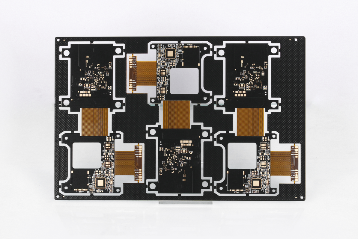
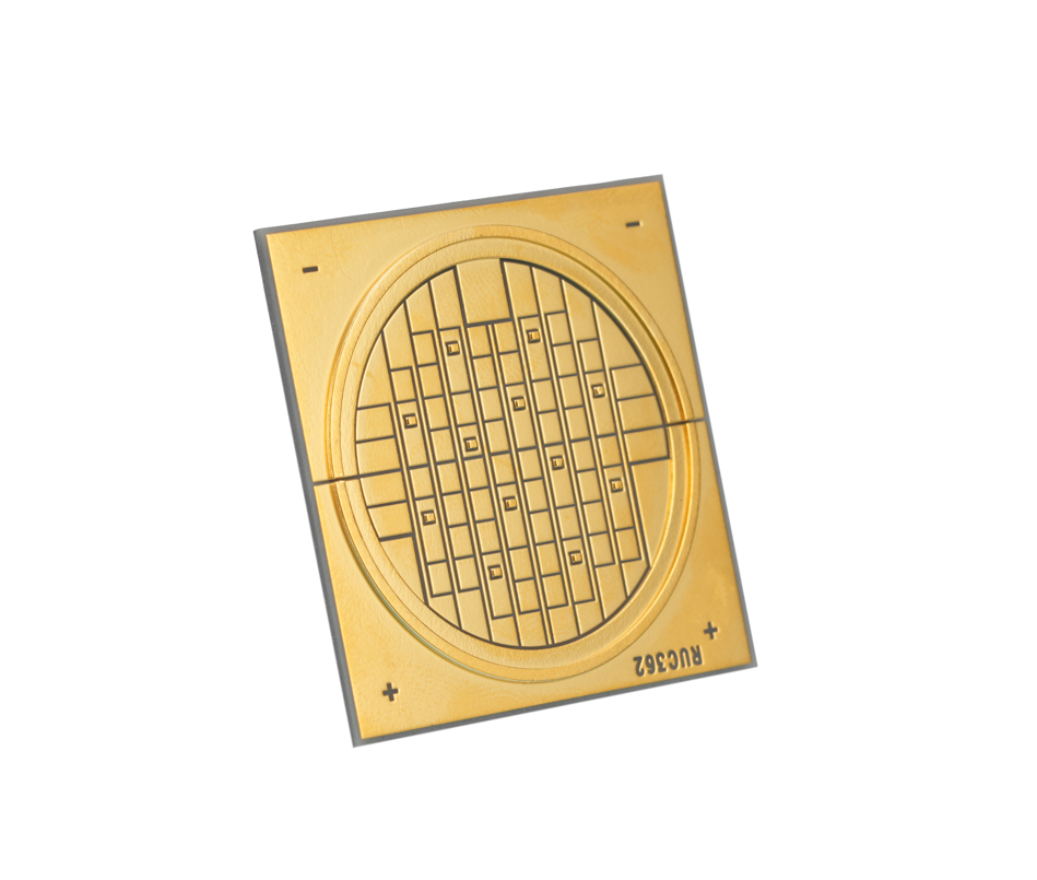
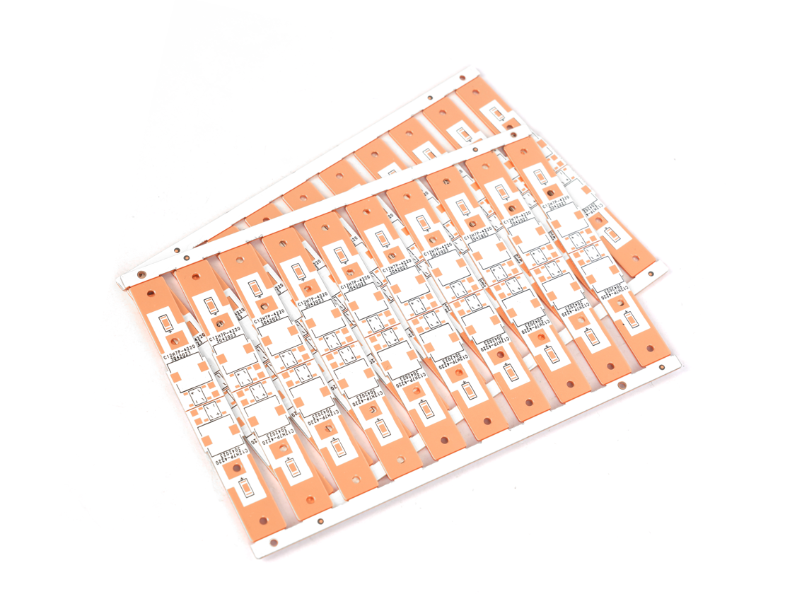
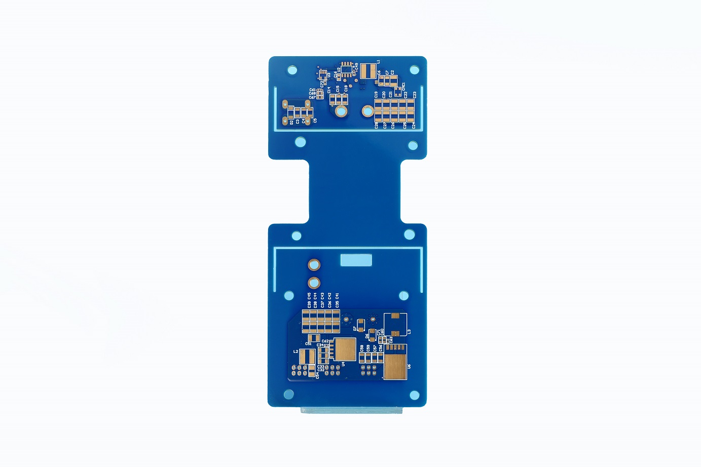
PCB manufacturing PCB manufacturing
Home > Blog

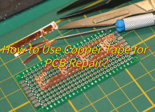
How to Use Copper Tape for PCB Repair?

September 5th, 2025

How to use copper tape for PCB repair? Let’s explore benefits, applications, usage process, tools and material list, copper tape types, testing methods, and maintenance tips for copper tape PCB repair.

As a professional PCB manufacturer, EBest Circuit (Best Technology) can provide you PCB repair service:

  • Free Technical Support: Provide evaluation of repair alternatives.
  • Repair multilayer boards: Supports blind and buried hole conductivity.
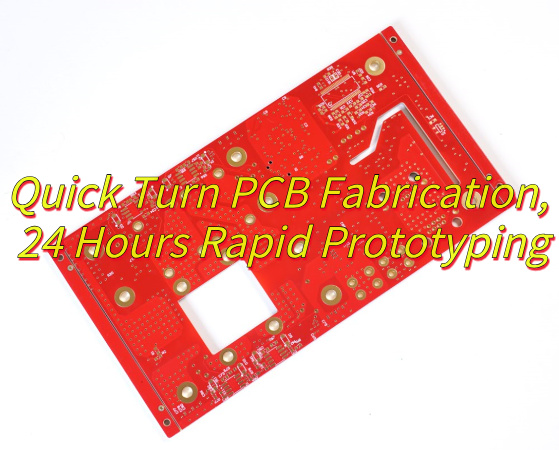
  • 24 Hours Rapid Prototyping: Quickly replace the broken PCB board.

Welcome to contact us if you have any request for PCB repair or PCB prototyping: sales@bestpcbs.com.

Why Choose Copper Tape for PCB Repair?

Reasons why choose copper tape for PCB repair:

Fast Repairs, Save Time

  • No need for complex tools or long waits, just cut and stick the copper tape, then solder. Perfect for fixing broken traces or lifted pads quickly.
  • Great for emergencies or prototyping, reducing equipment downtime.

Excellent Conductivity, Stable Signals

  • Pure copper with conductive adhesive ensures low resistance (usually ≤50mĪ©), matching original circuit performance.
  • Avoids signal issues caused by poor connections.

Flexible and Easy to Use

  • Bend and cut copper tape to fit tight spaces or complex PCB layouts (e.g., keyboard circuits, sensors).
  • Less risk of short circuits compared to jumper wires.

Low Cost, High Value

  • Much cheaper than custom PCBs or professional repair services. Ideal for small batches or hobbyists.
  • One roll lasts for multiple repairs, offering long-term savings.

Versatile Applications

  • EMI Shielding: Reduces electromagnetic interference.
  • Quick Prototyping: Test circuit designs without remanufacturing PCBs.
  • Grounding: Provides reliable ground connections for components.

Works with Most PCB Materials

  • Suitable for FR-4, CEM-1, and other common substrates, as well as gold-plated or ENIG finishes.
  • Strong adhesive holds up under high temperatures (compatible with reflow soldering).
Why Choose Copper Tape for PCB Repair?

Applications of Copper Tape PCB Repair

  • Fix Broken Traces: Layer copper tape over cut or damaged traces and solder ends.
  • Replace Lifted Pads: Stick copper tape where pads detached; solder components to it.
  • Bridge Missing Connections: Use tape to jump gaps where traces are missing.
  • Reinforce High-Stress Areas: Add tape to flexed PCB zones (e.g., connectors) to prevent breaks.
  • Quick Prototyping: Temporarily modify or add circuits without etching new PCBs.
  • EMI Shielding: Cover sensitive parts with tape to block interference.
  • Ground Components: Create low-resistance ground paths for noise reduction.
  • Repair Keyboard Membranes: Patch broken conductive traces on flexible keyboard circuits.
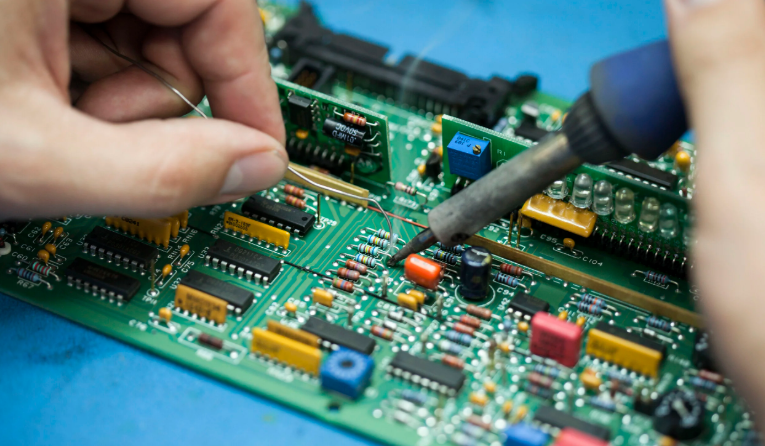
Applications of Copper Tape PCB Repair

How to Use Copper Tape for PCB Repair?

Below are steps of copper tape for PCB repair:

1. Inspect and Clean the Damaged Area

  • Visually locate the broken trace. Use a magnifier to confirm the damage range.
  • Clean the area with an alcohol-soaked cotton swab to remove residue, oxidation, or solder mask. If the solder mask covers the break, scrape it off with a blade or sandpaper to expose the copper base.

2. Cut the Copper Tape

  • Trim the tape to match the broken trace’s shape, ensuring it’s slightly larger than the damaged zone (covering intact copper on both ends).
  • The tape width should match the original trace. Length must span the break and overlap adjacent copper (at least 1-2mm).

3. Apply the Copper Tape

  • Press the tape flat onto the break, ensuring full contact with exposed copper and no air bubbles.
  • The tape must fully cover the break and extend to nearby pads or vias for reliability.

4. Solder to Secure

  • Quickly solder the tape’s ends to the PCB copper. Avoid overheating (back adhesive may melt).
  • Use low-temperature solder. Keep the iron’s contact time under 2 seconds to prevent tape detachment.
  • If repairing a pad, solder the component lead to the tape simultaneously.

5. Trim Excess Tape

  • Carefully cut or scrape the tape edges to match the original trace width.
  • Warning: The repair is fragile—avoid excessive force to prevent lifting.

6. Reinforce and Insulate

  • (Optional) Cover the tape with insulating tape (e.g., Kapton) or apply solder mask to prevent shorts or damage.
  • For high-stress areas (e.g., PCB edges), reinforce with epoxy (e.g., Araldite).

7. Test Functionality

  • Use a multimeter to check continuity (resistance should be near 0Ī©).
  • Power on the device and monitor for poor contact or overheating.

Copper Tape for PCB Repair Tools & Material List

Tool/MaterialPurpose
Single-Sided Conductive Copper Foil TapeBridge broken traces, repair pads, restore copper foil.
Isopropyl Alcohol (IPA) + SwabsClean oxidation, flux residue, or solder mask from repair area.
Fiber Pen/Engraving KnifeMark repair zone or scrape solder mask covering breaks.
Soldering Iron (250–300°C)Solder copper tape to PCB traces for low-resistance contact.
Lead-Free Solder WireReinforce joints to reduce contact resistance.
Hot Air Gun (80–100°C)Soften adhesive for better tape adhesion (optional).
Scissors/Precision KnifeTrim tape edges to match trace width; prevent field concentration.
600-Grit SandpaperLightly abrade copper for improved adhesion (oxidized areas only).
Conformal Coating/UV MaskInsulate and protect repair from oxidation/shorts.
Kapton TapeSecondary insulation for tape edges; high-temp resistant.
Epoxy Resin (e.g., Araldite)Reinforce high-stress areas (edges, connectors).
Multimeter (Resistance Mode)Verify continuity (resistance ā‰ˆ 0Ī©); check for abnormal heating post-repair.

Types of Copper Tape Suitable for PCB Repair

1. Single-Sided Conductive Copper Foil Tape

  • Use: Fix broken traces, repair missing pads, fill copper foil defects.
  • Application: General PCB repairs, such as signal line breaks or component pin detachment.

2. Double-Sided Conductive Copper Foil Tape

  • Use: Cross-layer conductive connections (e.g., shielding repairs), multilayer board grounding.
  • Application: requiring bidirectional conductivity, like high-frequency circuit shielding or shorting between layers.

3. High-Temperature Copper Foil Tape

  • Use: Repairs in high-temperature environments (e.g., power modules, LED driver boards).
  • Application: Fixing lines near heat-generating components or temporary patching for reflow soldering.

4. Ultra-Thin Copper Foil Tape (≤10μm)

  • Use: High-density PCB repairs (e.g., BGA pad rework, fine-pitch traces).
  • Application: Precision fixes in tight spaces to avoid interference with component installation.

5. Corrosion-Resistant Zinc-Plated Copper Foil Tape

  • Use: Repairs in humid or corrosive environments (e.g., outdoor equipment, industrial control boards).
  • Application: Extend repair lifespan in salt-fog or moisture-heavy conditions.

6. Non-Conductive Adhesive Copper Foil Tape

  • Use: High-voltage circuit repairs (e.g., power board isolation), insulating layer patches.
  • Application: Where adhesive must not create electrical contact to prevent shorts.

    Testing and Verifying Repaired PCB Functionality

    1. Visual Check

    • Look for visible flaws on the repaired PCB, like solder bridges, cold joints, or damaged parts.
    • Confirm components are placed and oriented correctly as per the design.

    2. Continuity Test

    • Use a multimeter to check electrical continuity between key points, e.g., power/ground traces and component connections.
    • Ensure no open or short circuits exist.

    3. Power-Up Test

    • Connect PCB to power supply and slowly raise voltage to operating level.
    • Watch power consumption; check for abnormal current or voltage issues.

    4. Function Test

    • Create and run a full test plan covering all PCB functions.
    • Use tools like logic analyzers or oscilloscopes to verify digital and analog circuit operation.
    • Test under different conditions (voltages, frequencies, loads) for stability.

    5. Signal Test

    • For high-speed or sensitive signals, check for crosstalk, reflections, and jitter.
    • Use TDR or similar methods to analyze signal quality.

    6. Thermal Test

    • Monitor PCB and component temperatures during operation; ensure they’re within limits.
    • Use thermal cameras or sensors to find hot spots or excessive heat.

    7. Environment Test

    • Put PCB through stress tests like temperature cycling, humidity, and vibration.
    • Confirm it still works after each test with no degradation.
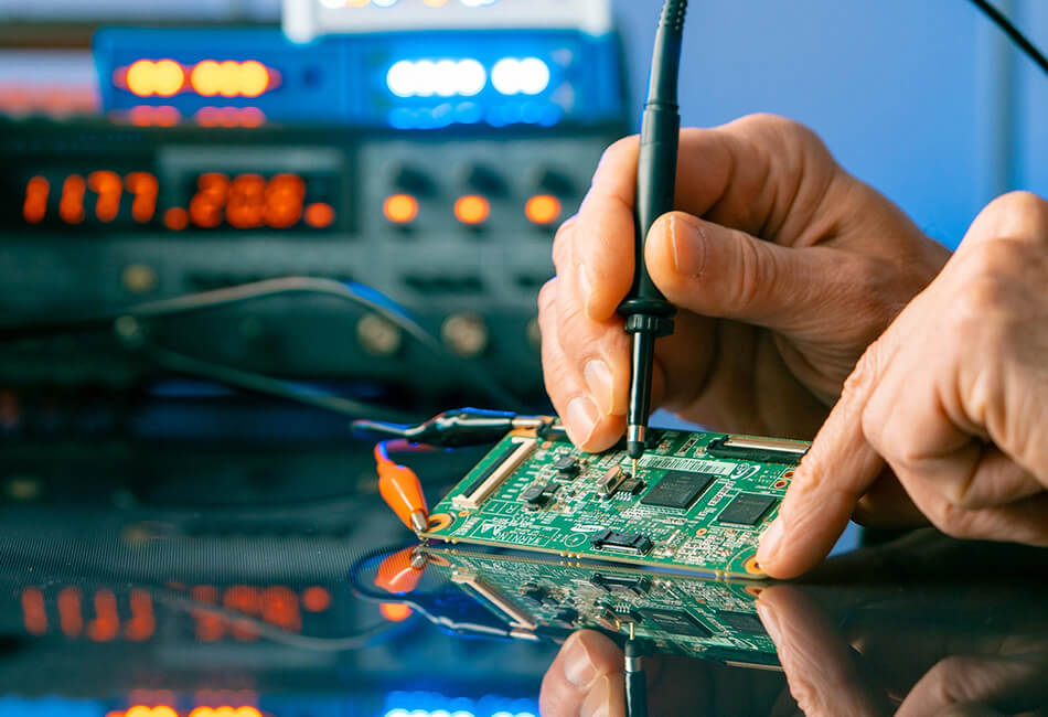
    Testing and Verifying Repaired PCB Functionality

    Long-Term Maintenance Tips for Copper Tape Repairs

    1. Keep It Clean

    • Wipe the repair area with a dry cloth to remove dust.
    • Use isopropyl alcohol (90%+) and a cotton swab for spills, avoid scrubbing.

    2. Block Moisture

    • Coat the copper tape with non-conductive epoxy or conformal coating.
    • Store/operate PCBs in a dry place (<60% humidity).

    3. Avoid Bending/Pressure

    • Don’t flex or twist flexible PCBs near the repair.
    • Keep heavy objects off the repaired area.

    4. Check for Corrosion

    • Inspect every 3–6 months for discoloration or lifting edges.
    • Test with a multimeter for unexpected resistance.

    5. Strengthen High-Use Joints

    • Add solder to frequent connections for durability.
    • Secure tape edges with non-conductive glue/epoxy.

    6. Avoid Extreme Temps

    • Keep repairs away from heat sources (e.g., motors).
    • Prevent rapid cold exposure to avoid condensation.

    7. Track Repairs

    • Label the repair site (e.g., “R12 – Copper Fix”).
    • Log dates/issues in a maintenance notebook.

    8. Replace if Needed

    • If the tape cracks, corrodes, or peels, remove and reapply a new piece.

      FAQs of Copper Tape for PCB Repair

      Q1: Why does copper tape for PCB repair peel off?
      A1: Clean the PCB with alcohol and a cloth. Use strong-adhesive copper tape and press firmly with a flat tool.

      Q2: Why do copper tape connections cut in and out?
      A2: Press out air bubbles with a smooth tool. Add solder to key spots after sticking the tape for better contact.

      Q3: Why does copper tape cause shorts or breaks?
      A3: Line up the tape carefully using a magnifier. Hold it in place with masking tape before pressing down.

      Q4: Why does copper tape corrode or dull?
      A4: Coat the repair with epoxy or conformal coating to block moisture. Store extra tape in a dry, sealed spot.

      Q5: Why are solder joints on copper tape weak?
      A5: Use low heat when soldering and avoid overheating. Clean off flux residue with alcohol after soldering.
      You may also like

      Quick Turn PCB Fabrication, Rapid Prototyping

      September 3rd, 2025

      What is quick turn PCB fabrication? Let’s discover its technical spec, design strategies, production process, recommended manufacturer.

      Are you worried about these issues?

      • Delays stalling R&D?
      • Low-cost quality risks?
      • Hidden costs inflating budgets?

      EBest Circuit (Best Technology) can provide service:

      • 48-hour full-cycle delivery.
      • 98%+ first board pass rate.
      • All-inclusive pricing.

      Welcome to contact us if you have any request for quick turn PCB: sales@bestpcbs.com.

      What Is Quick Turn PCB Fabrication?

      Quick Turn PCB Fabrication is a highly efficient printed circuit board (PCB) production service. Through optimized processes, automated design checks, and synchronized production management, it completes the entire process from design to delivery within 24 hours to 5 days, significantly shortening product development cycles.

      This service is designed to rapidly respond to the electronics industry’s needs for prototype verification and urgent production, allowing for flexible design adjustments. While the unit price is higher, it improves overall efficiency by saving time and costs. This service is widely used in consumer electronics prototypes (such as IoT devices), emergency medical and automotive parts, and rapid verification for startups.

      Technical Specifications for Quick Turn PCB Fabrication

      Parameter CategoryTechnical Specifications
      Layer Count1-16 layers (standard)
      18-32 layers (advanced)
      Substrate TypesFR-4 (standard) / High-Tg FR-4 / Polyimide / PTFE (RF) / Aluminum-backed
      Copper Thickness0.5oz(17μm)/1oz(35μm)/2oz(70μm)/3oz(105μm) (outer layers)
      0.5oz-2oz (inner layers)
      Min Trace/Space3mil(0.075mm)/4mil(0.1mm)/5mil(0.125mm) (standard)
      2mil(0.05mm) (laser drilling)
      Via TechnologyThrough-hole(PTH)/Blind(BVH)/Buried(BVH)
      Microvia(≤0.15mm)
      Surface FinishesHASL(Leaded/Lead-free)/ENIG/OSP/Immersion Silver/Immersion Tin
      Solder Mask CoverageGreen(standard)/Blue/Red/White/Black/Clear (LPI)
      Dimensional ToleranceBoard edges: ±0.15mm
      Hole diameters: ±0.05mm
      Outline: ±0.2mm (laser cutting)
      Special ProcessesGold fingers/Carbon ink printing/Embedded resistors/Rigid-flex/Selective gold plating
      Lead TimeSingle/double-sided: 24 hours
      4-8 layers: 48-72 hours
      10+ layers: 5-7 business days

      How to Design Fast Turn PCBs to Reduce Production Cost?

      1. Modular Pre-layout

      • Decompose complex circuits into independent functional modules (e.g., power modules, signal processing modules), develop standardized libraries for cross-project reuse. Universal power module packaging reduced layout time by 30%.

      2. Structured Constraint Management

      • Import mechanical structure data (STEP format), define keep-out zones and height restrictions. Use 25mil sub-grid for critical components (BGA) and 50mil main grid for general layout to align with automated SMT machine precision.

      3. Layer Count Dynamic Balancing

      • Determine minimum viable layer count through signal integrity simulation. Replace traditional through-holes with buried/blind via hybrid structures for high-speed signals. Reduced an 8-layer industrial control board to 6 layers, cutting costs by 18%.

      4. Material Standardization Strategy

      • Prioritize FR-4 substrate, use localized PTFE hybrid construction for >5GHz signals. Develop enterprise material libraries with ≄70% standard component packages. Achieved 40% cost reduction compared to full Rogers 4350B solutions.

      5. DFM Rules Embedded Design

      • Implement real-time DRC rules: minimum trace width/spacing 6mil, pad diameter via+12mil, solder mask opening trace+4mil. Reduced production defect rates from 2.3% to 0.7%.

      6. Panelization Economic Design

      • Use V-cut + stamp hole hybrid panelization with 3mm process margin. Optimal panel count: 5pcs/panel, reducing unit costs by 35% versus single boards.

      7. Concurrent Design Process

      • Execute parallel tasks during schematic phase: BOM standardization review, ECAD-MCAD mechanical interference checks, and FloTHERM thermal simulations. Shortened design cycles from 15 days to 9 days.
      How to Design Fast Turn PCBs to Reduce Production Cost?

      Double Sided PCB Quick Turn Fabrication Processes

      1. Material Cutting

      • Substrate Preparation: Use automatic shearing machines to cut copper-clad laminates (FR-4/CEM-1) into standard sizes (e.g., 18″Ɨ24″) with edge tolerance ≤0.1mm.
      • Pre-Baking Treatment: Bake cut substrates at 120ā„ƒ for 2 hours to eliminate material stress and prevent warpage during subsequent processes.

      2. Drilling

      • CNC Drilling: Employ 6-axis CNC drills with 0.2mm–3.2mm diameter bits, operating at 10,000–15,000rpm. Drilling time per panel ≤5 minutes.
      • Hole Cleaning: Immediately blow debris from holes using high-pressure air to avoid plating defects.

      3. Electroless Copper Plating

      • Desmearing: Immerse drilled panels in potassium permanganate solution to remove resin residues from holes.
      • Copper Deposition: Deposit 0.3–0.5μm copper layer in alkaline solution for hole wall conductivity, taking ~45 minutes.

      4. Circuit Imaging

      • Dry Film Lamination: Attach photosensitive dry film to substrates via thermal rollers at 110ā„ƒĀ±5ā„ƒ and 1.5m/min speed.
      • Laser Exposure: Use LDI (Laser Direct Imaging) to project patterns onto dry film with ≤4mil resolution, eliminating film usage and saving 30% time.

      5. Etching

      • Alkaline Etching: Immerse exposed panels in ammonium chloride-copper solution to remove non-conductive copper, maintaining line width tolerance ±0.05mm.
      • Quick Stripping: Rinse residual dry film with high-pressure water jet at 50ā„ƒĀ±5ā„ƒ for ≤2 minutes.

      6. Solder Mask Application

      • Screen Printing: Apply UV-curable solder mask using 36T mesh, achieving 20–30μm thickness with automatic alignment accuracy ±0.1mm.
      • Pre-Curing: Bake panels at 80ā„ƒ for 10 minutes in infrared tunnel oven to stabilize ink flow.

      7. Surface Finish

      • Nickel deposition: 3–5μm thickness, 8–12 minutes
      • Gold deposition: 0.05–0.1μm thickness, 3–5 minutes
      • Alternative: HASL (Hot Air Solder Leveling) through tin furnace, taking ≤1 minute per panel.

      8. Electrical Testing

      • Flying Probe Testing: Utilize 4-axis flying probe machines with 50–150g contact force. Single panel testing time ≤3 minutes, covering 100% networks.
      • Fault Marking: Automatically ink-mark short/open circuit locations for rework.

      9. Routing & Depaneling

      • CNC Milling: Cut panels using 1mm diameter milling bits with ±0.05mm path accuracy. Single board routing time ≤2 minutes.
      • V-Cutting: For manual breakaway, score panels to 1/3 thickness at 30°–60° angle.

      10. Final Inspection & Packaging

      • AOI Inspection: Scan solder pads/traces with 3D cameras to detect defects (e.g., solder balls, misalignment) at 1.2m²/minute speed.
      • Vacuum Packaging: Seal panels in aluminum foil bags with desiccant, vacuuming to -0.1MPa for moisture/oxidation protection.
      Double Sided PCB Quick Turn Fabrication Processes

      Why Choose EBest Circuit (Best Technology) as Quick Turn PCB Manufacturer?

      Reasons why choose us as quick turn PCB manufacturer:

      • Ultra-Fast Delivery (24-72 Hours): Accelerates product development cycles by 50%+ compared to standard lead times, enabling rapid prototyping and market validation.
      • Advanced Technical Capabilities: Supports 1-16 layer boards with 0.1mm mechanical drilling and 0.1mm laser microvias. Minimum 3.5mil/4mil trace/space (1mil/1mil for HDI). Enables complex designs for IoT, wearables, and high-speed applications.
      • Automated DFM Checks: Reduces design errors by 30%+ through pre-production validation, minimizing rework costs.
      • Transparent Pricing Model: Eliminates hidden costs, with small-batch discounts for prototypes <50pcs.
      • 24/7 Engineering Support: Real-time technical assistance during design phase prevents costly production delays.
      • ISO-Certified Quality Control: Ensures reliability for medical/automotive applications with zero-defect tolerance.
      • Surface Finish Flexibility: HASL, ENIG, OSP options with 2μm gold thickness control.

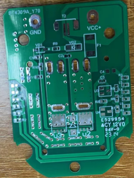
      Below is a photo of FR4 PCB board we made before:

      Why Choose EBest Circuit (Best Technology) as Quick Turn PCB Manufacturer?

      Our Quick Turn PCB Prototyping Time

      LayersNormal ServiceFastest Service
      17 Days24 H
      28 Days24 H
      410 Days48 H
      610 Days72 H
      812 Days72 H
      ≄10TBDTBD

      Our Quick Turn PCB Options

      1. Express Delivery (24-48 Hours)

      • Layer Support: 1-6 layers (standard boards).
      • Trace Width/Spacing: 3.5mil/4mil (1mil/1mil for advanced processes).
      • Drill Size: 0.2mm mechanical drilling (0.1mm laser microvias).
      • Suitable For: Urgent prototype verification, exhibition samples.

      2. Standard Quick Turn Service (3-5 Days)

      • Layer Support: 8-10 layers (complex designs).
      • Material Options: FR-4, aluminum substrate, high-frequency materials (Rogers/PTFE).
      • Surface Finishes: HASL (leaded/lead-free), ENIG, OSP.
      • Suitable For: Small-batch trial production, functional testing.

      3. Economy Quick Turn Solution (5-7 Days)

      • Copper Thickness: 0.5oz-3oz (standard options).
      • Solder Mask Colors: Green, Blue, Red, Black, White, Matte Black.
      • Cost Optimization: Volume discounts (50+ panels).
      • Suitable For: Pre-production validation, cost-sensitive projects.

      How to Get A Quote for Quick Turn PCB Project?

      Follow these steps to ensure accurate and efficient quotation:

      1. Submit Design Files

      • Provide Gerber files (RS-274X format) or PCB design source files (Altium/Eagle/PADS).
      • Include assembly drawings if applicable.

      2. Specify Technical Requirements

      • Layer count (1-16 layers).
      • Minimum trace width/spacing (e.g., 3.5mil/4mil).
      • Drill size requirements (mechanical/laser).
      • Material type (FR-4, aluminum, Rogers/PTFE).

      3. Confirm Production Details

      • Order quantity (5-5,000+ pieces).
      • Surface finish preference (HASL/ENIG/OSP).
      • Copper thickness (0.5oz-6oz).
      • Solder mask color selection.

      4. Indicate Special Requirements

      • Impedance control needs.
      • Blind/buried vias requirement.
      • High-frequency material certification.
      • RoHS compliance requirement.

      5. Provide Contact Information

      • Company name and location.
      • Project timeline expectations.
      • Preferred communication channel (email/phone).

      Welcome to contact us if you have any request for quick turn PCB: sales@bestpcbs.com.

      You may also like

      PCB Directory Types: FR4, FPC, Ceramic & Metal Core PCB

      September 2nd, 2025

      Would you like to know what types of PCB directory are? Let’s explore FR4, Flexible, ceramic and metal core PCB directories through this blog together.

      At EBest Circuit (Best Technology), we can provide you service:

      • Competitive Price & Premium Quality– Maximize your budget with cost-effective PCBs that meet stringent quality standards.
      • 24 Hours Rapid Prototyping– Accelerates product development cycles.
      • Free ā€ŒDFM (Design for Manufacturabilityā€Œ) Support -Prevents manufacturing errors before production.
      • Full Turnkey Solution-handle PCB fabrication to assembly, saving vendor coordination time cost and production cost.

      Feel free to contact us if you have any inquiry for FR4 PCB, FPC PCB, ceramic PCB and MCPCB: sales@bestpcbs.com.

      What Is PCB Directory?

      PCB Directory is a professional online service platform dedicated to the global printed circuit board (PCB) industry. It aggregates resources from manufacturers, assembly providers, and design service firms, facilitating efficient supplier matching through parameter-based categorization (e.g., material type, layer count, thickness) and geographic filters. The platform supports specialized requirements such as flexible PCB and ceramic PCB, streamlining supply chain collaboration in electronics manufacturing and serving as a critical industry information hub.

      What Is PCB Directory?

      What Are Types of PCB Directory?

      Base Material Categories

      1. FR4 PCB Directory

      • Core Material: Fiberglass-reinforced epoxy composite.
      • Parameters: Tg 130-180ā„ƒ, DK 4.2-4.8.
      • Applications: Consumer electronics mainboards, industrial control systems.

      2. Flexible PCB (FPC) Directory

      • Core Material: Polyimide (PI) or polyester film.
      • Technical Features: Bend radius ≤1mm, >100,000 flex cycles.
      • Applications: Foldable smartphones, medical endoscopy devices.

      3. Ceramic PCB Directory

      • Material Systems: Alā‚‚Oā‚ƒ (96%), AlN, BeO.
      • Thermal Performance: AlN 170-230W/mĀ·K > Alā‚‚Oā‚ƒ 24-28W/mĀ·K.
      • Applications: High-power LED modules, aerospace radar systems.

      4. Metal Core PCB(MCPCB) Directory

      • Structural Types: Aluminum-backed (MCPCB), Copper-backed (IMS).
      • Thermal Management: Thermal resistance as low as 0.5ā„ƒ/W.
      • Applications: Automotive headlamp drivers, photovoltaic inverters.

      FR4 PCB Directory

      • Single Layer PCB
      • 2 Layers PCB
      • Multi-Layer PCB
      • Heavy Copper PCB
      • Bus Bar PCB
      • Extra Thin PCB
      • High Tg PCB
      • HDI PCB
      • RF Board

      Our FR4 PCB capabilities:

      ItemCapabilities
      Layer Count1 – 32 Layers
      Max Board Dimension2424″ (610610mm)
      Min Board Thickness0.15mm
      Max Board Thickness6.0mm – 8.0mm
      Copper ThicknessOuter Layer: 1oz~30oz, Inner Layer: 0.5oz~30oz
      Min Line Width/Line SpaceNormal: 4/4mil (0.10mm); HDI: 3/3mil (0.076mm)
      Min Hole DiameterNormal: 8mil (0.20mm); HDI: 4mil (0.10mm)
      Min Punch Hole Diameter0.1″ (2.5mm)
      Min Hole Spacing12mil (0.3mm)
      Min PAD Ring(Single)3mil (0.075mm)
      PTH Wall ThicknessNormal: 0.59mil (15um); HDI: 0.48mil (12um)
      Min Solder PAD DiameterNormal: 14mil (0.35mm); HDI: 10mil (0.25mm)
      Min Solder mask BridgeNormal: 8mil (0.2mm); HDI: 6mil (0.15mm)
      Min BAG PAD Margin5mil (0.125mm)
      PTH/NPTH Diameter TolerancePTH: ±3mil (0.075mm); NPTH: ±2mil (0.05mm)
      Hole Position Deviation±2mil (0.05mm)
      Outline ToleranceCNC: ±6mil (0.15mm); Die Punch: ±4mil (0.1mm); Precision Die: ±2mil (0.05mm)
      Impedance ControlledValue>50ohm: ±10%; Value≤50ohm: ±5ohm
      Max Aspect Ratio0.334027778
      Surface TreatmentENIG, Flash Gold, Hard Gold Finger, Gold Plating(50mil), Gold finger, Selected Gold plating, ENEPIG, ENIPIG; HAL, HASL(LF), OSP, Silver Immersion, Tin Immersion
      Solder mask ColorGreen/White/Black/Yellow/Blue/Red

      FPC PCB Directory

      • Single Sided Flexible Circuits
      • Double Sided Flexible Circuits
      • Multilayer Flexible Circuits
      • ā€ŒFFC(Flat Flexible Cableā€Œ)
      • Dual Access Flexible Circuits
      • Rigid-Flex Circuits

      Our FPC PCB capabilities:

      ItemCapabilities
      Layers Count1-10L
      Max Board Dimension1L:500*2000mm; 2L:250*1380mm
      Conductor Thickness1/3 OZ (12 um) – 4OZ (140um)
      Min Line Width/Line Space2/2mil
      Min Hole SpacingNPTH:16mil; PTH:20mil
      Hole Position Deviation±4mil (0.10mm)
      Outline ToleranceLaser: +0.15mm/-0.05mm;
      Die Punch: +0.10/-0.20 mm
      Surface TreatmentENIG(Au 4u”), Hard Gold Plating (Au 50u”), Immersion Silver, Immersion Tin, OSP, ENEPIG
      FPC PCB Directory

      Our rigid-flex circuits capabilities:

      ItemCapabilities
      Layers Count2-50L
      Max Board Dimension500 Ɨ 500mm
      Conductor Thickness0.5oz (18μm) – 2oz (70μm)
      Board Thickness0.3mm – 4.0mm
      Min Line Width/Line Space4/4mil
      Min Hole SpacingNPTH: 16mil; PTH: 20mil
      Min Solder Mask Bridge8mil
      Impedance Controlled±10% (>50Ī©); ±5Ī© (≤50Ī©)
      Rigid-Flex Circuits

      Ceramic PCB Directory

      • Thick Film Ceramic PCB
      • Thin Film Ceramic PCB
      • DBC Ceramic PCB
      • DPC Ceramic PCB
      • AMB Ceramic PCB
      • LTCC PCB
      • HTCC PCB

      Our ceramic PCB capabilities:

      ItemCapabilities
      Layer Count    1-6L (Thick Film)
      1-2L (DBC/DPC/AMB)
      4-64L (LTCC/HTCC)
      Substrate MaterialAlā‚‚Oā‚ƒ, AlN, BeO, ZrOā‚‚, Siā‚ƒNā‚„
      Conductor ThicknessCopper: 0.035-0.30mm
      AgPd: 10-20μm
      Au: 6-10μm
      Working Temperature-50ā„ƒ to 800ā„ƒ
      Bonded Resistors±0.5% Tolerance
      PTH Diameter Tolerance±4mil (0.1mm)
      NPTH Diameter Tolerance±2mil (0.05mm)
      Outline ToleranceLaser: +0.20/-0.05mm
      Max Board SizeThick Film: 200Ɨ200mm
      DBC/DCB: 138Ɨ178mm
      DPC: 138Ɨ190mm AMB: 114Ɨ114mm
      Min Board Thickness0.25mm-0.40mm
      Min Hole SpacingNPTH: 16mil (0.30mm)
      PTH: 20mil (0.5mm)
      Hole Vias Tolerance±4mil (0.1mm)
      Cutting ToleranceLaser: +0.2/-0.05mm
      Mold+0.25/-0.20mm
      Line Width/Space Tolerance±5mil (0.125mm), ±1mil (0.025mm)
      Surface TreatmentAgPd, AuPd, Mn/Ni (Thick Film), OSP, Nickel Plating, ENIG, ENEPIG
      Ceramic PCB Directory

      Metal Core PCB Directory

      • Aluminum Base PCB
      • Copper Base PCB
      • COB PCB
      • SinkPAD PCB

      Our MCPCB capabilities:

      ItemCapabilities
      Layer Count1-10L
      Max Board Dimension610Ɨ1625mm
      Conductor Thickness0.5oz – 10oz
      Min Line Width/Line Space4/4mil
      Wall Copper ThicknessNormal: 0.59mil; HDI: 0.48mil
      Special Hole TypesCounterbore hole, Countersunk hole, Blind, Buried, Vias
      Max Aspect Ratio10:1
      Min Board Thickness0.8mm
      Max Board Thickness5.0mm
      Min Hole Diameter0.8mm
      Min Hole Spacing1mm
      Min Solder mask Bridge0.15mm
      Metal Core PCB Directory

      Our Prototyping Lead Time

      Lead time for FR4 PCB prototyping

      LayersNormal ServiceFastest Service
      17 Days24 H
      28 Days24 H
      410 Days48 H
      610 Days72 H
      812 Days72 H
      ≄10TBDTBD

      Lead time for MCPCB prototyping

      LayersNormal ServiceFastest Service
      14 Days24 H
      214 Days168 H
      421 DaysTBD

      Lead time for FPC, Rigid- Flex & Ceramic PCB Prototyping

      ItemsNormal ServiceFastest Service
      FPC48-72 H24 H
      Rigid- Flex2 Weeks for 4L1.5 Weeks for 4L
      >4L: TBD>4L: TBD
      Ceramic3 Weeks2 Weeks

      Our Quality Certifications

      • ISO9001:2015
      • ISO13485:2016
      • REACH
      • RoHS
      • IATF16949

      Attaches is our FR4 PCB prototype video for your reference:

      Welcome to contact us if you need any help for FR4 PCB, FPC PCB, ceramic PCB and MCPCB : sales@bestpcbs.com.

      You may also like

      What is TFT PCB? TFT LCD PCB

      August 30th, 2025

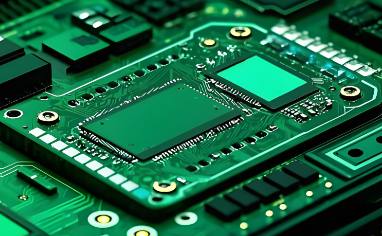
      When you look at your smartphone, car navigation screen, or even a medical monitor, you’re looking through a TFT display. TFT, which stands for Thin Film Transistor, is a technology that allows precise control of millions of pixels, producing sharp images and vibrant colors. Yet, behind the glass layer of the display lies something equally important—the TFT PCB.

      The TFT PCB is the printed circuit board that supports and controls the TFT display module. Without it, the panel is just passive glass, unable to light up or show an image. The PCB provides the ā€œintelligenceā€ that makes the display come alive. It manages signals, regulates power, drives the backlight, and often integrates the touch interface.

      Understanding how TFT PCBs function is essential not only for engineers but also for product developers, purchasing managers, and anyone working with display modules. Let’s explore what a TFT PCB is, how it works, where it’s used, and why choosing the right manufacturing partner is vital.

      What is TFT PCB? TFT LCD PCB

      What is a TFT PCB in a Display?

      At its core, a TFT PCB is the electronic backbone of a TFT display module. The TFT display consists of two main parts:

      • The TFT glass – This contains the thin film transistors that control liquid crystal molecules, determining how light passes through each pixel.
      • The TFT PCB – This supports the TFT glass by supplying power, processing signals, and controlling the backlight.

      Think of the TFT glass as the screen canvas, and the TFT PCB as the control center. The glass defines the resolution, pixel density, and visual quality, but without the PCB, there’s no way to convert system signals into images.

      For example, a 7-inch automotive TFT screen may have a resolution of 1024Ɨ600. The TFT glass determines the number of pixels, but it’s the PCB that drives each of those pixels according to the instructions from the car’s mainboard.

      How Does a TFT PCB Work?

      The TFT PCB works like an interpreter between the system and the display. Its tasks can be divided into three major functions:

      1. Signal Processing

      The host device—whether a smartphone, industrial controller, or infotainment system—sends digital image data. But this data needs to be formatted into instructions that control each pixel.

      • Signal Input: Common formats include LVDS, eDP, or MIPI DSI.
      • Driver ICs: These chips on the PCB decode the signals and decide how each pixel should behave.
      • Row and Column Control: Signals are distributed row by row and column by column, activating specific transistors on the TFT glass.

      For example, when displaying a red dot in the corner of a smartphone screen, the PCB’s driver ICs calculate which pixels to energize and how to modulate them to show red.

      2. Power and Backlight Management

      TFT displays require several power rails: one for the logic, one for the glass, and one for the LED backlight.

      • Voltage Regulation: The PCB includes regulators to maintain stable voltages, typically ranging from 1.8V for logic to 12V for backlight.
      • Backlight Control: LED drivers adjust brightness through PWM (Pulse Width Modulation) or current control. This makes it possible to dim the screen for night use or boost brightness for outdoor visibility.

      Without these circuits, the display would flicker, show unstable images, or fail to achieve uniform brightness.

      3. Touch Controller Integration

      In many TFT modules, the PCB also supports the touch layer.

      • Capacitive Touch Controllers: Sense changes in capacitance when a finger touches the screen.
      • Resistive Touch Controllers: Detect pressure applied on the surface.

      The PCB processes these touch signals and communicates them back to the main system.

      This is how swiping on your smartphone screen or tapping a medical device control panel is translated into action.

      What are the Key Components on a TFT PCB?

      Although the PCB looks small, it’s packed with vital parts. Let’s look at them in detail:

      • Driver ICs: Often fine-pitch chips that directly control pixel rows and columns. They are critical for image sharpness and color accuracy.
      • Power ICs: Convert input power into the different voltage levels needed by the display and touch controller.
      • Backlight Circuitry: Includes LED drivers, current regulators, and protection circuits.
      • Touch Controller: Only present in touch-enabled displays. Handles finger tracking, multi-touch, and gesture recognition.
      • Connectors and FPCs: Provide the bridge between the PCB and the host system. For slim devices, flexible printed cables (FPCs) are widely used.
      • Oscillators and Timing Circuits: Ensure that signals reach the glass in perfect sync.

      In high-end automotive or medical displays, additional components may be added, such as temperature sensors, EMI filters, and redundant power circuits for safety.

      What are the Key Components on a TFT PCB?

      What are the Applications of TFT PCBs?

      TFT PCBs are used in nearly every industry where visual information is needed. Some of the most common applications include:

      • Consumer electronics – Smartphones, tablets, laptops, TVs.
      • Automotive – Digital dashboards, navigation systems, entertainment screens.
      • Industrial equipment – Control panels, human-machine interfaces (HMIs).
      • Medical devices – Patient monitors, diagnostic equipment.
      • Aerospace and defense – Rugged displays with high visibility and durability.

      In each application, the PCB is customized to meet specific requirements, whether it’s compact size, heat resistance, or EMI shielding.

      What are the Design Considerations for TFT PCBs?

      Designing a TFT PCB is more challenging than many other PCB types because of the high-speed signals, compact layouts, and strict reliability needs.

      1. High-Speed Signal Integrity

      TFT PCBs often carry LVDS, MIPI DSI, or eDP signals that run in the hundreds of megahertz.

      • Impedance Control: Differential traces are routed with controlled impedance, usually 90 Ī© ± 10%.
      • Length Matching: Signal pairs are length-matched to avoid skew.
      • Grounding and Shielding: Reference planes are carefully planned to minimize crosstalk.

      2. Power Distribution and Stability

      • Multiple Rails: A single TFT PCB may require 1.8V, 3.3V, 5V, and 12V simultaneously.
      • Filtering: LC filters smooth power for sensitive circuits.
      • Decoupling Capacitors: Placed close to ICs to reduce noise and voltage dips.

      3. Thermal Management

      • Backlight Heat: LED backlights generate heat. Copper pours, thermal vias, and sometimes aluminum-backed designs are used.
      • IC Heat Dissipation: High-power driver ICs may need thermal pads to spread heat across the PCB.

      4. Mechanical and Form Factor Constraints

      • Thickness: Many handheld devices demand ultra-thin PCBs (as low as 0.4 mm).
      • Flexibility: For foldable devices, the PCB must endure repeated bending.
      • Mounting Holes: Carefully placed to avoid stress on the glass.

      5. Reliability for Harsh Environments

      • Automotive: Wide temperature (-40°C to 125°C), vibration-resistant designs.
      • Medical: Compliance with strict safety standards, including isolation for patient-connected devices.
      • Aerospace: Lightweight but highly reliable boards, often using advanced laminates.

      6. Cost vs Performance

      Every design choice affects cost.

      • More Layers = better performance, higher cost.
      • ENIG Finish = better for fine-pitch, but more expensive than OSP.
      • Hybrid Rigid-Flex PCB = saves space, but increases production difficulty.

      Example: A simple home appliance TFT PCB may use a 2-layer OSP-finished board. An automotive infotainment TFT PCB may require 8 layers with ENIG finish and redundant power circuits.

      How is a TFT PCB Manufactured?

      The production of TFT PCBs combines standard PCB processes with advanced assembly techniques:

      1. Material Selection: FR4 is the most common for rigid PCBs, while polyimide is used for flexible TFT modules.

      2. Copper Layering and Etching: Multiple copper layers are stacked and etched to create signal and power traces.

      3. Surface Mount Assembly: Components like driver ICs and regulators are mounted using automated SMT machines.

      4. Fine-Pitch Soldering: Since display connectors and ICs have extremely small pads, precision soldering is required.

      5. Testing: Includes electrical continuity, signal quality, and backlight performance checks.

      6. Reliability Validation: For critical industries, additional tests such as thermal cycling, humidity resistance, and vibration are conducted.

      The end result is a robust PCB that works seamlessly with the TFT glass, delivering both functionality and durability.

      What is the Difference Between TFT PCB and Other Display PCBs?

      Different display technologies require different PCB support.

      • TFT PCB vs OLED PCB: OLEDs are self-illuminating, so their PCBs mainly manage signals and power, while TFT PCBs must also handle backlight circuits.
      • TFT PCB vs LED Display PCB: LED display PCBs directly control thousands of LEDs in panels, often for outdoor or large-format use. TFT PCBs are designed for compact glass-based displays.
      • Cost Comparison: TFT PCBs are usually less expensive than OLED PCBs, making them a cost-effective choice for many industries.

      This is why TFT remains popular: it provides a balance between performance, cost, and maturity of technology.

      Why Choose EBest Circuit (Best Technology) for TFT PCB Manufacturing?

      As one of the best PCB manufacturers in China, our goal is to provide our customers with the best quality products and services at the most competitive pricing, and to become a reliable long-term partner of our customers in PCB manufacture and assembly.

      Since its establishment in 2006 as a printed circuit board manufacturer, EBest Circuit (Best Technology) has focused on high-quality, low to medium-volume PCB fabrication, PCB assembly and electronics manufacturing. Our products and services include 1-100 layers printed circuit boards, thru-hole assembly, SMT assembly including BGA assembly, components sourcing, turnkey box build and electronic product development. From consumer electronics to advanced aerospace displays, EBest Circuit (Best Technology) has the capability and expertise to support projects of any scale.

      FAQs

      1. What materials are used in a TFT PCB?

      Most TFT PCBs use FR4 for rigid sections and polyimide for flexible cables. Advanced materials may be used in high-frequency or high-reliability designs.

      2. Can TFT PCBs support touch screen functions?

      Yes. Capacitive or resistive touch controllers are often integrated into the PCB to handle user interactions.

      3. How thin can a TFT PCB be?

      Flexible TFT PCBs can be as thin as 0.15 mm, while rigid designs are typically 0.6–1.6 mm.

      4. Are TFT PCBs different for automotive displays?

      Yes. Automotive TFT PCBs are designed for durability, with heat-resistant materials, vibration tolerance, and wider operating temperature ranges.

      5. What is the typical cost of a TFT PCB?

      Costs vary based on size, layer count, and application. Consumer TFT PCBs are usually low-cost, while automotive and medical-grade boards cost more due to higher standards.

      You may also like

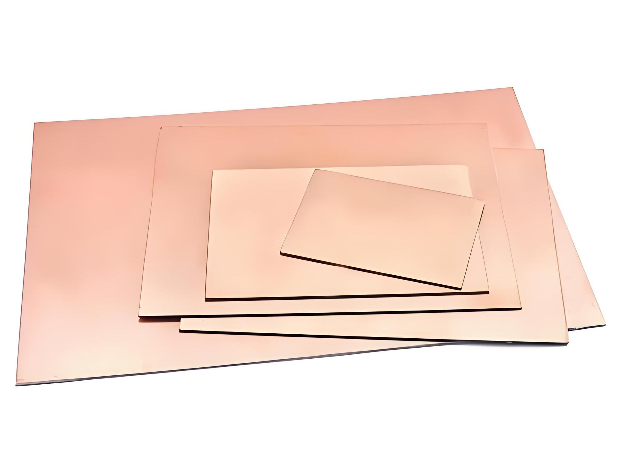
      What is a Copper Clad PCB? Copper Clad Laminate (CCL)

      August 21st, 2025

      Copper clad PCB are a core material for printed circuit boards (PCBs). Composed of an insulating substrate and copper foil, these materials are heat-pressed to form a composite. They both support components and provide conductive circuits. Depending on the substrate, these materials can be categorized as paper, fiberglass, composite, or metal. They are widely used in consumer electronics, communications, automotive, and industrial control applications.

      What is a Copper Clad PCB? Copper Clad Laminate (CCL)

      Are you curious about EBest Circuit (Best Technology)’s copper clad PCBs?

      • Does the insulation performance meet circuit insulation requirements?
      • Can the material strength withstand the processing and usage environment?
      • Is the performance and cost balance balanced?
      • Does BEST Technology provide customization and after-sales support?

      EBest Circuit (Best Technology)’s copper clad PCB can answer these questions.

      • Compatible. Supports standard sizes and customized specifications (thickness, shape), adapting to different PCB design requirements, and enabling fast response for small batches.
      • Performance. The base material is highly resistant to bending and impact, and can withstand cutting, drilling, and other processing processes, preventing cracking or deformation after long-term use.
      • Achieve. Performance meets industry standards, with over 100 board options for cost optimization, balancing reliability and affordability.
      • Provide. Supports customization of materials, specifications, and processes. After-sales service includes rapid response and warranty services, and expedited orders ship within 24 hours.

      What is copper clad in PCB?

      Copper clad PCB refers to a board where a thin layer of copper foil is bonded to one or both sides of a substrate, usually fiberglass or other insulating material. This copper layer forms the conductive surface where circuit patterns are later etched.

      Without this copper cladding, a PCB would just be an insulator with no ability to carry signals. By laminating copper onto the substrate, the board gains electrical conductivity and becomes the foundation for electronic circuits.

      The copper clad board is then processed through techniques like imaging, etching, and drilling to create pathways that allow electricity to flow between components.

      In short, a copper clad PCB board is the starting point for almost every PCB. It bridges the gap between insulating materials and conductive pathways.

      How thick is PCB copper clad?

      Copper thickness is one of the most critical specifications in any copper clad PCB sheet. It directly affects current-carrying capacity, heat dissipation, and durability.

      The thickness of copper in PCBs is usually measured in ounces per square foot (oz/ft²). Here’s what it typically looks like:

      • 0.5 oz/ft² copper → about 18 microns thick
      • 1 oz/ft² copper → about 35 microns thick
      • 2 oz/ft² copper → about 70 microns thick
      • 3 oz/ft² and above → heavy copper, often used for power electronics
      What is a Copper Clad PCB? Copper Clad Laminate (CCL)

      Standard consumer electronics often use 1 oz copper. High-power applications may need 2 oz or more to handle higher currents without overheating.

      So, when choosing a PCB copper clad board, thickness depends on your circuit’s power requirements and performance needs.

      What are the materials of copper clad laminate (CCL)?

      The copper clad laminate (CCL) is not just copper. It’s a composite material made of multiple layers. Each one has a specific role.

      Here are the primary materials used:

      1. Copper Foil

      • Conductive layer
      • Provides the pathways for current flow
      • Usually treated to improve adhesion

      2. Resin System

      • Often epoxy or modified epoxy
      • Acts as a binder
      • Provides mechanical strength

      3. Reinforcement Material

      • Fiberglass cloth is the most common
      • Ensures dimensional stability
      • Improves heat resistance

      4. Additives

      • Flame retardants
      • Fillers for mechanical stability
      • Special compounds for high-frequency applications

      The combination of these elements gives the copper clad laminate PCB its strong insulation, mechanical toughness, and long-term reliability.

      What is a PCB with copper clad on only one side called?

      PCB with copper laminated on only one side is known as a single-sided copper clad board. It’s the simplest form of PCB copper clad laminate.

      These are widely used in low-cost and less complex electronic devices. For example:

      • Calculators
      • Power supplies
      • LED lighting modules
      • Consumer gadgets

      On the other hand, a double sided copper clad PCB board has copper foil on both sides. This allows more complex designs and higher component density.

      Therefore, depending on the complexity of the circuit, a single-sided or double-sided option can be chosen.

      What are the types of copper clad laminate (CCL)?

      Copper clad laminates are available in different types to suit varied applications. Here are the main categories:

      What is a Copper Clad PCB? Copper Clad Laminate (CCL)

      Based on Substrate

      • Paper-based (phenolic resin) → Affordable, good for household appliances
      • Glass fabric (epoxy resin) → More durable, widely used in general electronics
      • Composite CCL → A mix of paper and fiberglass

      Based on Copper Foil

      • Electrolytic copper foil → Smooth surface, ideal for precision circuits
      • Rolled annealed copper foil → Excellent ductility, used in flexible PCBs

      Based on Application

      • General-purpose CCL → Cost-effective and widely used
      • High-frequency CCL → Designed for RF and microwave devices
      • High-speed CCL → Used in data communication systems
      • Thermal conductive CCL → Great for LED and power devices

      Each type of copper clad laminate PCB material is designed to handle unique performance demands.

      Why use a copper clad PCB board?

      Copper clad PCBs bring several advantages that make them a preferred choice:

      • Excellent Conductivity: Copper provides stable and reliable current flow.
      • Thermal Management: Thicker copper spreads heat efficiently, preventing damage.
      • Mechanical Strength: Fiberglass reinforcement adds stability.
      • Design Flexibility: Available in single, double, or multilayer forms.
      • Cost Efficiency: Paper-based and FR4 laminates reduce manufacturing costs.

      These advantages have led to the widespread use of copper clad PCBs in consumer electronics, automotive systems, and medical devices.

      What is copper clad used for?

      Copper clad boards serve as the base for many electronic products. Some key applications include:

      1. Consumer Electronics

      • Smartphones, tablets, laptops
      • Wearable devices

      2. Automotive Electronics

      • Control modules
      • Safety systems
      • Infotainment units

      3. LED Lighting

      • High thermal conductivity versions
      • Used in LED lighting aluminum substrates

      4. Industrial Control Systems

      • Robust designs for high current
      • Suitable for harsh environments

      5. Medical Devices

      • Compact and reliable circuits
      • Long-term performance stability

      In short, copper clad PCBs are used anywhere reliable electronic connections are required.

      How to choose a copper clad board for PCB?

      Choosing the right copper clad laminate PCB requires balancing performance, cost, and application needs. Here’s how you can decide:

      What is a Copper Clad PCB? Copper Clad Laminate (CCL)

      1. Power Requirements

      • High current? Choose thicker copper.
      • Low power? Standard 1 oz copper is enough.

      2. Frequency Performance

      • For RF or high-speed circuits, select low-loss laminates.
      • For simple circuits, FR4 is cost-effective.

      3. Thermal Demands

      • LEDs and power devices benefit from thermal conductive laminates.

      4. Design Complexity

      • Single-sided for simple devices.
      • Double-sided or multilayer for complex designs.

      5. Budget Considerations

      • Paper-based laminates are cheaper.
      • Glass-fiber laminates offer longer life.

      By considering these factors, you can select the best copper clad board PCB for your project.

      At EBest Circuit (Best Technology), we specialize in PCB copper clad laminates that meet international standards and deliver long-term reliability. If you are seeking a trustworthy supplier for your copper clad PCB boards, our team is here to help. Contact us today at sales@bestpcbs.com

      You may also like

      4-Layer Rigid Flex PCB Design & Manufacturer, Fast Delivery

      August 15th, 2025

      What is a 4-layer rigid flex PCB? Let’s explore its stackup, thickness, benefits, applications, design guide and manufacturing processes through this blog.

      Are you troubled with these issues?

      • Is the line impedance fluctuation exceeding the standard after the product is bent? (Precision impedance control is used on rigid-flex boards, ensuring fluctuations of <5% after bending)
      • Is stress concentration causing cracking during multi-module assembly? (A four-layer stepped transition design distributes 90% of mechanical stress)
      • Is crosstalk severe during high-speed signal transmission? (Embedded shielding layer + differential pair routing, crosstalk suppression -50dB)

      EBest Circuit (Best Technology) can provide service:

      • Intelligent DFM Platform: Automatically detects design flaws and generates 3D assembly simulation videos
      • Hot-Compression Process Library: Provides six compression profiles, increasing yield to 99.2%
      • Full-Process Dashboard: Real-time display of 12 process statuses, including substrate cutting, lamination, and electroplating

      Welcome to contact us if you have any request for rigid flex PCB: sales@bestpcbs.com.

      What Is a 4-Layer Rigid Flex PCB?

      The 4-Layer rigid flex PCB is a composite board made by combining a flexible printed circuit board (FPC) and a rigid printed circuit board (PCB) through a special process, which has the characteristics of both. Its core structure usually includes a four-layer design, with the middle two layers being flexible areas and the two sides being rigid areas. The rigid-flex combination is achieved through a lamination process.

      What Is a 4-Layer Rigid Flex PCB?

      4 Layer Rigid Flex PCB Stackup

      • Layer 1 (Top): Rigid signal layer (routing + key components)
      • Layer 2 (Inner Layer 1): Flexible ground layer (PI substrate, providing shielding and mechanical support)
      • Layer 3 (Inner Layer 2): Flexible signal layer (low-speed/auxiliary signals, optimizing routing density)
      • Layer 4 (Bottom): Rigid power/ground plane (FR4, reducing noise coupling)

      How thick is a 4-Layer Rigid Flex PCB?

      A 4-layer rigid-flex PCB typically has a total thickness range of 0.8mm to 1.6mm, depending on the design requirements and material combinations. Rigid sections (FR4) usually measure 1.2mm thick, providing structural support. Flex sections (polyimide) are much thinner, commonly 0.1mm, allowing bending and flexibility. The overall thickness is influenced by the copper weight (e.g., 1oz for signal layers, 2oz for power/ground planes) and dielectric material (FR4 or prepreg) used in the stackup.

      Why Use 4-Layer Rigid Flex PCB?

      Advantages of 4-layer rigid flex PCB:

      • Space and Routing Optimization: A layered design separates signal and power planes, increasing wiring density and making it suitable for compact devices like smartphones.
      • Signal and Electromagnetic Performance: Adjacent power/ground layers reduce noise, and thick inner copper ensures stable high-speed signal transmission.
      • Efficient Thermal Management: The inner copper foil evenly dissipates heat, and thermal vias enhance reliability in high-temperature environments.
      • Mechanical and Durability: A rigid-flexible structure reduces bending failures, and a multi-layered, vibration-resistant design is suitable for industrial applications.
      • Design and Cost Balance: Customized stacking optimizes performance and cost, while eliminating cables and streamlining the assembly process.
      Why Use 4-Layer Rigid Flex PCB?

      When to Use 4 Layer Rigid Flex PCB?

      Applications of 4 Layer Rigid Flex PCB:

      • High-Density Electronic Devices – Smartphones, tablets, and wearables requiring compact layouts with dynamic bending zones.
      • Automotive Electronics – Dashboard control units and sensors exposed to vibration and temperature fluctuations.
      • Medical Devices – Implantable monitors and portable diagnostics needing lightweight, biocompatible designs.
      • Aerospace Systems – Avionics and satellite components demanding weight reduction and shock resistance.
      • Industrial Robotics – Articulated arms with repeated motion joints requiring durable yet flexible interconnections.
      • Consumer Electronics – Foldable displays and rotating-camera mechanisms necessitating 3D PCB solutions.

      How to Design a 4-Layer Rigid Flex PCB?

      Here are 4-layer rigid flex PCB design guide:

      1. Layer Stackup & Material Selection

      • Rigid Zones: Use FR4 substrate (1.6mm thickness) for structural integrity.
      • Flex Zones: Opt for polyimide substrates (e.g., DuPont Pyralux AP/LF/FR) with 0.1–0.3mm thickness to accommodate dynamic bending.
      • Copper Type: Rolled Annealed (RA) copper for flex layers to ensure ≄100,000 bend cycles.
      • Coverlay: Match coverlay thickness to copper weight (0.5oz Cu → 1mil coverlay; 1oz Cu → 1.5mil coverlay).

      2. Bend Radius Calculation

      • Formula: Minimum bend radiusĀ R=tƗK, whereĀ tĀ = total flex-zone thickness,Ā KĀ = layer-dependent coefficient (single-layerĀ K=6–10; dual-layerĀ K=10–15; four-layerĀ K=20–50).
      • Example: For a 0.29mm four-layer flex zone, dynamic bend radius must be ≄5.8mm to prevent copper cracking.

      3. Routing & Impedance Control

      • Signal Layer Allocation: Place high-speed signals (e.g., DDR, PCIe) on outer layers (L1/L4); use inner layers (L2/L3) for power/ground planes.
      • Trace Rules: Follow IPC-2223 standards (e.g., 70µm trace width/90µm spacing for 0.5mm BGA).
      • Microvias: Use laser-drilled microvias (≤0.1mm diameter) with copper-filled construction (IPC-4761 Type VII).

      4. Mechanical & Thermal Design

      • Transition Zones: Implement “key-and-slot” designs or plastic frames to reduce stress concentration at rigid-flex junctions.
      • Thermal Management: Use ≄1oz copper in power/ground planes; add thermal via arrays (spacing ≤1mm) for heat dissipation.
      • Component Reinforcement: Add stiffeners (Kapton or aluminum, <10mil thickness) under flex-zone components to mitigate soldering stress.

      5. Manufacturing & Testing Standards

      • IPC Compliance: Meet IPC-6013 Class 3/A requirements via 100% electrical testing, AOI, and X-ray inspection.
      • Reliability Tests: Conduct thermal shock (-40°C to 125°C), vibration (≄20G random), and bend cycle (≄1000 iterations) validations.
      How to Design a 4-Layer Rigid Flex PCB?

      How to Make a 4-Layer Rigid Flex PCB?

      Below are 4-Layer rigid flex PCB manufacturing processes:

      Flexible Circuit (Flex) Processing

      1. Shearing: Cut raw flex material (e.g., polyimide w/ copper) to size.
      2. Drill: Use CNC to drill holes for layers/connections (4 – layer flex → holes for interlayer links).
      3. PTH: Plate copper inside drilled holes (electro/electroless plating) for layer connectivity.
      4. Dry Film Lamination: Apply photosensitive dry film (heat/pressure) as etching mask.
      5. Develop: UV – expose film, wash off unexposed areas.
      6. Etch: Remove unmasked copper (acid bath) to form traces.
      7. Strip: Chemically remove remaining dry film.
      8. AOI: Scan for defects (opens, shorts, wrong trace widths) via automated optical inspection.

          Rigid Circuit (Rigid) Processing

          1. Shearing: Trim raw rigid material (e.g., FR – 4) to panel size.
          2. Drill: CNC – drill holes for components/vias.
          3. Dry Film Lamination: Apply dry film (heat/pressure) as etching mask.
          4. Develop: UV – expose, wash unexposed film.
          5. Etch: Acid – etch unmasked copper to create traces.
          6. Strip: Remove leftover dry film.
          7. AOI: Check for defects (bad traces, opens/shorts) with automated optics.

          Flex + Rigid Integration

          1. 2nd Drill: Add holes for final connections (flex – rigid alignment, new vias).
          2. De – Burr: Remove drill burrs (brush/chemical).
          3. De – smear: Clean drill residues from holes (solvent/plasma).
          4. PTH: Plate copper in new holes (electro/electroless) for cross – layer links.
          5. DES: Repeat develop/etch/strip to shape integrated traces (flex + rigid).
          6. AOI: Verify no misalignments/shorts between flex + rigid sections.
          7. Solder mask: Apply liquid polymer, UV – expose, develop to protect non – solder areas.
          8. Surface Finish: ENIG/ HASL
          9. Silkscreen: Print ink (stencils) for labels, part markers.

            Final Assembly

            1. 2nd Pressing: Bond stiffeners (if needed) via heat/pressure.
            2. Flex + Rigid Align: Use fixtures/optics to align flex + rigid sections.
            3. FQC: Final visual/dimensional check (no misalignments, good solder mask).
            4. Coverlay: Laminate protective film (polyimide) on flex areas (heat/pressure).
            5. 2nd Drill: Add final holes (connectors, mounting).
            6. Outline Rout: Cut board to final shape (CNC routing/punching).
            7. PCB Separate: Split multi – panel boards (routing/punching).
            8. E – Test: Check for opens/shorts/impedance issues.
            9. Stiffener Attach: Add mechanical supports (if needed) to flex zones.
            10. Packing: Seal in anti – static bags/trays (protect from damage/ESD).

            How to Make a 4-Layer Rigid Flex PCB?

            Why Choose EBest Circuit (Best Technology) as Rigid Flex PCB Manufacturer?

            • International Certifications: ISO 9001/UL/IATF 16949/RoHS certified, with medical-grade ISO 13485 support.
            • High-End Technical Capabilities: Supports 32-layer board design with a minimum line/space width of 0.0762mm, compatible with HDI and high-frequency materials (such as Rogers RO4350B).
            • High-Quality Materials: The flexible area utilizes DuPont polyimide substrate with rolled copper (≄100,000 flex cycles) to ensure durability.
            • Strict Quality Inspection: 100% electrical testing + AOI + X-ray inspection, compliant with IPC-6013 Class 3/A, with impedance control accuracy of ±5%.
            • 24 Hours Rapid Prototyping: Standard orders are completed within 7 days, expedited orders within 3 days, with two free prototype verifications per month.
            • Flexible Custom Design: Supports 4-layer rigid + 2-layer flex stack-ups, blind and buried vias, metal edges, and other special processes.
            • Free Technical Support: Design-for-Function (DFM) checks and optimization, with 24/7 engineer assistance for impedance matching and thermal management.
            • Cost-effective solution: Tiered pricing for bulk orders (e.g., 6-ply panels at $200/10), and intelligent panelization reduces material waste by 15-20%.
            • End-to-End Service: Support rigid-flex PCB prototyping, design, manufacturing, assembly service and help you reduce time and production cost a lot.

            Our Rigid-Flex PCB Capabilities

            Parameter CategoryParameter NameParameter Value
            Flexible Layer CountLayer Range1-10 layers
            ConfigurationBonded or Air Gap
            Rigid Layer CountLayer Range1-40 layers
            Total Layer CountLayer Range2-50 layers
            Flexible Core MaterialMaterial TypePolyimide (PI)
            Thickness Range0.5 mil to 4 mils
            Adhesive ConstructionAdhesive or Adhesiveless
            Copper ThicknessFlexible Circuit1/3 oz – 2 oz (RA or ED Copper Foil)
            Rigid Circuit0.5 oz to 10 oz
            CoverlayMaterial TypePolyimide (PI)
            Thickness Range0.5 mil to 2 mils
            Stiffener MaterialMaterial TypePolyimide (PI), FR4, Stainless Steel, Aluminum
            Rigid MaterialMaterial TypeFR4 (TG 130/170/180), Low Flow Prepreg
            EMI/RF ShieldingShielding FilmEMI/RF Shielding Films
            Special Via StructuresBlind Vias & Buried ViasSupported
            Any Layer InterconnectSupported
            Controlled ImpedanceImpedance Values50Ī©, 90Ī©, 100Ī©, 110Ī©, and Custom Values
            Surface FinishingProcess TypesENIG, ENEPIG, Gold Plating, Gold Fingers (3-30Āµā€ Au), Immersion Silver
            IPC StandardCertification LevelsIPC 6013 Class II & Class III Available

            How Can I Get a Quote for a 4 Layer Rigid-Flex PCB?

            Essential Documents to Submit for Quotation

            1. Gerber Files

            • Include all layers (L1-L4) in 274X format with drill files.
            • Specify rigid/flex zones and bend areas in layer notes.

            2. Stackup Diagram

            • Detail material thickness (e.g., FR4 for rigid, polyimide for flex).
            • Copper weight (e.g., 1oz inner layers, 0.5oz flex zones).

            3. Technical Specifications

            • Board dimensions (±0.1mm tolerance).
            • Min. trace/space (e.g., 4/4mil for rigid, 5/5mil for flex).
            • Surface finish (e.g., ENIG, immersion gold).

            4. Special Requirements

            • Impedance control (e.g., ±10% for 50Ī© signals).
            • Stiffener locations (e.g., FR4 at connector areas).

            5. Quantity & Lead Time

            • Prototype (5-10pcs) or bulk order (e.g., 1k pcs/month).
            • Urgency (standard 15 days or expedited 7 days).

            Contact EBest Circuit (Best Technology) with your project details for a competitive quote for rigid-flex PCB needs: sales@bestpcbs.com.

            You may also like

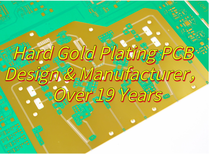
            Hard Gold Plating PCB Design & Manufacturer, Over 19 Years

            August 12th, 2025

            What is hard gold plating PCB? Let’s discover its definition, plating thickness, spec, benefits, applications, design guide, production process together.

            Are you worried about these issues?

            • Is high-frequency signal transmission loss high? (Hard Gold Plating PCB’s extremely low resistivity ensures signal integrity.)
            • Is connector contact wear leading to failure? (Hard Gold Plating PCB’s wear-resistant plating has a lifespan over 5 times longer.)
            • Is poor soldering causing soaring after-sales costs? (Hard Gold Plating PCB’s smooth plating achieves 100% soldering yield.)

            EBest Circuit (Best Technology) can provide services and solutions:

            • Customized Plating Thickness: Adjust the gold layer thickness (1-5μm) based on current load requirements to avoid excessive cost.
            • Full-Process Impedance Control: Comprehensive control from substrate to plating ensures high-frequency impedance fluctuations of less than 5%.
            • Mass Production Stability Guarantee: Utilizing automated plating lines and AOI quality inspection, batch-to-batch hardness variation is ≤10HV.

            Welcome to contact us if you have any request for hard gold plating PCB: sales@bestpcbs.com.

              What Is Hard Gold Plating PCB?

              Hard Gold Plating PCBā€Œ is a special process that electroplates a high-hardness gold alloy (such as gold-cobalt or gold-nickel alloy) on the surface of the PCB pads or contact points. It is characterized by the high hardness of the gold layer (150-300HV) and strong wear resistance, making it suitable for applications with frequent plugging and unplugging or mechanical friction (such as connectors, key switches, etc.).

              Compared with traditional soft gold plating (pure gold), hard gold plating improves durability through the nickel base and alloy composition, but the welding difficulty is slightly higher. This process complies with industry standards (such as IPC-4552) and is a key technology to ensure the long-term reliability of high-end electronic equipment.

              What Is Hard Gold Plating PCB?

              PCB Hard Gold Plating Thickness

              PCB hard gold plating thickness is typically controlled within the range of 0.05–0.5 microns (50–500 nanometers). This thickness is precisely controlled through the electroplating process, ensuring excellent conductivity, oxidation resistance, and wear resistance (for example, gold-cobalt alloy plating can achieve a hardness of 150–300 HV), while balancing cost and soldering reliability. Too thin a thickness may result in insufficient wear resistance, while too thick a thickness increases costs and compromises soldering performance.

              PCB Hard Gold Plating Thickness

              Hard Gold Plating PCB Specification

              Parameterā€Œā€ŒSpecificationā€Œ
              ā€ŒGold Thicknessā€Œ0.05~0.15μm
              ā€ŒHardnessā€Œ60~120HV
              ā€ŒWear Resistanceā€Œā‰„500 cycles
              ā€ŒSurface Roughnessā€Œā‰¤0.2μm Ra
              ā€ŒAdhesionā€ŒPass Cross-cut (≄4B)
              ā€ŒSolderabilityā€ŒIPC J-STD-003
              ā€ŒResistivityā€Œā‰¤0.05Ω·cm²
              ā€ŒOperating Tempā€Œ-55ā„ƒ~125ā„ƒ

              Advantages of Hard Gold Plating PCBs

              • Ultra-Long-Life Design: With a hardness of 60-120 HV, its wear resistance is five times greater than soft gold, ensuring long-term, stable operation of high-frequency plug-in components (such as connectors) and reducing replacement costs.
              • Guaranteed Zero Signal Loss: Resistivity ≤ 0.05Ω·cm², it’s perfectly compatible with 5G/RF modules, reducing signal attenuation and improving device communication reliability.
              • Risk-Free Soldering: Passed the 100-grid test (≄4B), temperature-resistant from -55°C to 125°C, and exhibits zero delamination after soldering, making it suitable for high-reliability applications such as medical and aerospace.
              • Precision Manufacturing Compatibility: Surface roughness ≤ 0.2μm Ra supports fine-pitch assembly such as BGA/CSP, improving yield and reducing production failures.
              • Global Compliance: Compliant with RoHS and IPC-4552B standards, its lead-free process meets European and American environmental regulations, simplifying the export certification process.
              Advantages of Hard Gold Plating PCB

              Applications of Hard Gold Plating PCB

              • High-frequency communications equipment – 5G base stations, radio frequency modules, and satellite communication systems.
              • Automotive electronics – On-board sensors, ECU control units, and high-speed connectors.
              • Military and aerospace – Radar systems, satellite payloads, and avionics equipment.
              • Medical devices – Implantable devices, endoscopic probes, and high-precision monitors.
              • Industrial automation – Robotic control panels, industrial sensors, and test probes.

              Hard Gold Plating PCB Design Guide

              Below is hard gold plating PCB design guide:

              1. Material and Substrate Selection

              • Prioritize FR-4 substrates for general applications; use low-loss materials (e.g., Rogers) for high-frequency/high-speed signals. For high-temperature or medical devices, opt for BT resin or polyimide (PI).
              • Copper foil thickness: 18μm (0.5oz) to 35μm (1oz) for standard traces; ≄70μm (2oz) for high-current applications.

              2. Plating Area Definition and Layout

              • Restrict hard gold plating to high-wear zones (e.g., gold fingers, connector contacts, keypads). Clearly mark plating regions to avoid unnecessary costs.
              • Eliminate sharp angles in plated areas; use rounded transitions (radius ≄0.3mm). Maintain ≄0.15mm (6mil) spacing between adjacent plated zones.

              3. Design Rules and Parameters

              • Minimum trace width/spacing: ≄4mil (0.1mm); ≄6mil (0.15mm) for dense layouts. Optimize differential traces with impedance calculators (e.g., Polar SI9000).
              • Pad dimensions: Ensure pads exceed component leads (single-side extension ≄0.25mm). Use oval/oblong pads for high-density designs. Fully enclose through-hole pads; add teardrops for double-sided boards.
              • Plating thickness: 1.27μm (50μin) to 2.54μm (100μin) per IPC-4552. Critical contacts (e.g., gold fingers) require ≄1.5μm for ≄10,000 insertion cycles.

              4. Manufacturability (DFM)

              • Define plated areas in CAD with copper overlap (minimum 500μm/20mil). Keep non-connected copper ≄800μm (31.5mil) from board edges.
              • Avoid overlapping plated zones with SMT/BGA pads. Add ≄12mil (0.3mm) wide traces to gold fingers for current balance.
              • Include test points for critical signals (e.g., clocks, power): diameter ≄1.8mm (70.8mil); spacing ≄2.5mm (100mil).

              5. Environmental and Reliability Requirements

              • Plating must pass 24-hour salt spray tests. Avoid acidic/alkaline exposure; apply protective coatings if needed.
              • Reserve thermal relief for high-power zones or use metal-core substrates (e.g., aluminum). Validate material CTE to prevent delamination or pad cracks.

              6. Standards and Compliance

              • Plating thickness: Follow IPC-4552 (hard gold ≄1.27μm). Electrical performance: Meet IPC-6012 (Class 2/3).
              • Confirm fabricator capabilities (e.g., min trace width, plating precision) upfront. Provide Gerber/drill files with clear plating annotations.

              7. Testing and Validation

              • Plating ductility: Pass ≄5% elongation in tensile tests. Verify thickness via XRF.
              • High-speed signals: Perform TDR for impedance control. Measure contact resistance (≤50mĪ©) with four-wire methods.

                Hard Gold Plating PCB Manufacturing Process

                1. Cutting

                  • Use a CNC cutter to cut the copper-clad laminate (e.g., FR-4) to the designed dimensions with an accuracy of ±0.1mm. Ensure smooth edges and no burrs.

                  2. Drilling

                    • Use a CNC drill to drill holes according to the Gerber file, with diameters ranging from 0.1mm to 3mm. After drilling, clean the hole walls to remove debris and oil.

                    3. Inner Layer Imaging

                      • Clean and roughen the copper-clad laminate surface to enhance dry film adhesion.
                      • The inner layer circuit pattern is covered with hot press dry film (temperature 100-120°C, pressure 3-5kg/cm²).
                      • Use UV light exposure (energy 80-150mJ/cm²), and remove the unexposed dry film with a developer (concentration 1%-3%, temperature 30-35°C).
                      • Etch the unprotected copper foil with an acidic etchant (concentration 1-2 mol/L, temperature 40-50°C) to form the circuits.

                      4. Lamination

                      • The copper foil surface is treated to a tan color (thickness 0.5-1.5 μm) to enhance adhesion to the prepreg.
                      • The inner layer is laminated to the prepreg according to the designed number of layers, with a positioning error of ≤±0.05 mm.
                      • Lamination is performed at high temperature (180-220°C) and high pressure (200-400 psi) for 60-120 minutes to form a multilayer structure.

                      5. Hole Metallization

                      • The hole walls are activated using a palladium salt solution (concentration 0.1-0.3 g/L, temperature 30-40°C, time 3-5 minutes), adsorbing palladium atoms as catalytic centers.
                      • A copper layer is formed on the hole walls by electroless copper plating (copper sulfate 10-20 g/L, formaldehyde 5-10 g/L, pH 11-13, time 30-60 minutes).

                      6. External Layer Imaging

                      • The process is similar to the inner layer, but requires additional lead plating. Use GPM-220 antistatic gold dry film, with a secondary dry film applied only to the pad area (2 mils larger than the solder mask).

                      7. Pattern Plating

                      • Hard gold plating uses a gold-cobalt alloy (cobalt content <0.2%), while soft gold is pure gold.
                      • Note: Gold thickness exceeding 4 μm cannot be achieved. Pad spacing is adjusted based on the gold thickness (e.g., a 0.38 μm gold thickness requires ≄7 mils).

                      8. Etching

                      • Acidic etching solutions will corrode unprotected copper foil to ensure trace accuracy.

                      9. Solder Mask & Screen Printing

                      • Apply photosensitive solder mask ink, then expose and develop it to form a protective layer (20-50 μm thick).
                      • Screen-print component identification; the ink must be abrasion-resistant and corrosion-resistant.

                      10. Hard Gold Plating

                      • Full-board plating: Dry film protects the non-plated areas, with secondary dry film applied only to the window pads.
                      • Localized plating: Lead design (e.g., 12mil-wide traces) with dummy gold fingers to isolate current and prevent thickness variations.

                      11. Outline Processing & Testing

                      • Using V-cut or milling technology, create the PCB outline with a tolerance of ±0.1mm.
                      • Electrical testing (conductivity, insulation), impedance testing (according to design requirements), and environmental testing (high temperature, high humidity, high temperature).

                      12. Final Inspection

                      • Appearance inspection (no scratches or oxidation).
                      • Dimensional measurement (error ≤ ±0.1mm).
                      • Gold thickness testing (Knoop hardness ≄90) and adhesion testing.
                      Hard Gold Plating PCB Manufacturing Process

                        Why Choose EBest Circuit (Best Technology) as Hard Gold Plating PCB Manufacturer?

                        Reasons why choose us as hard gold plating PCB manufacturer:

                        • Extremely Fast Delivery Guarantee: Urgent orders are processed within 24 hours, precisely meeting the urgent project delivery needs of the electronics industry and ensuring the timeliness of critical equipment R&D or repair.
                        • Strict Quality Control System: Full-process inspection is implemented for batch orders, ensuring a gold plating thickness tolerance of ±5% and a defect rate of less than 0.1%, ensuring highly reliable connections and long-term corrosion resistance.
                        • 19 Years of Technology: Leveraging 19 years of experience in precision circuit manufacturing, we efficiently address complex issues such as exposed copper in the hole wall and blackened gold surface during the gold plating process, ensuring plating uniformity and adhesion.
                        • Transparent Cost Optimization: Utilizing a no-hidden-cost pricing model combined with automated process optimization, we achieve cost savings of 15-20% compared to the industry average, making it particularly suitable for small and medium-volume orders.
                        • Free DFM Design Optimization: Free Design for Manufacturability (DFM) analysis is provided to proactively avoid issues such as improper gold plating area design and solder mask window errors, reducing rework costs by up to 30%.
                        • High First-Time Pass Rate Guarantee: 98% of samples pass customer acceptance on the first test, reducing iterative revisions due to substandard gold plating thickness or soldering performance issues, saving time and money.
                        • 24/7 Technical Response: 24/7 real-time support from our engineering team quickly resolves unexpected issues during the gold plating process, such as oxidation and micro-shorting, ensuring production continuity.
                        • Flexible Measurement Capability: Supports small-batch prototype verification of 1-10 units to large-scale production of over 10,000 units, meeting the full cycle from R&D prototyping to mass production.
                        • Global Standard Compliance: Complies with international standards such as IPC-6012, UL 94V-0, and RoHS. The gold plating layer has passed ASTM B488 salt spray testing, ensuring compliance for high-end applications in medical, aviation, and other fields.
                        • Compatible with various post-processing processes: In addition to hard gold plating, multiple surface treatment options such as HASL, ENIG, OSP, and immersion silver are also available to meet the needs of different welding processes (such as high-frequency signal transmission, high-precision placement, etc.).

                        Welcome to contact us if you have any inquiry for hard gold plating PCB: sales@bestpcbs.com.

                        You may also like

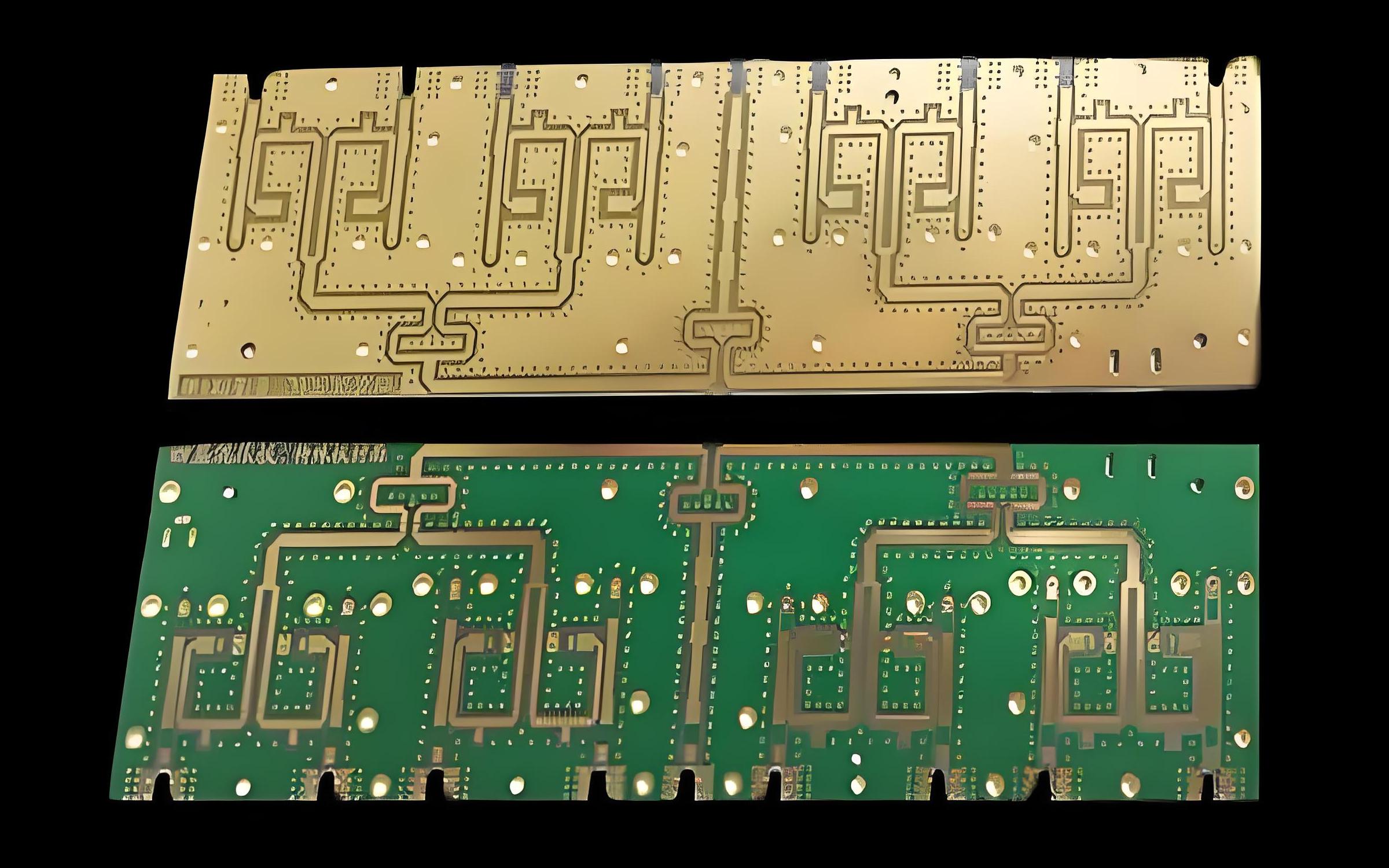
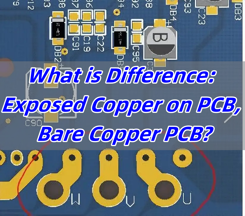
                        What is Difference: Exposed Copper on PCB, Bare Copper PCB?

                        August 1st, 2025

                        Exposed copper on PCBĀ is often seen in circuit designs where certain copper areas are left uncovered. These areas serve specific functions, especially for soldering or electrical connections. Knowing how this differs from a bare copper PCB helps you choose better solutions for your needs.

                        EBest Circuit (Best Technology) has been manufacturing PCBs and providing PCBA service to a very crowded market for over 19 years. We have a competitive edge in this area through precision processing and the customization capability, our all-process quality control system, as well as through delivery efficiency and the full turnkey EMS PCB service. Our engineering team has rich and valuable experience in optimizing exposed copper on PCB performance, improving the solderability, and the heat dissipation. There is no MOQ limit; you can enjoy the prototype, small quantity trial order, or large volume mass production service. We have the project managers to follow your project. If there is any engineering project, we will give feedback to you to avoid errors and repeated work.

                        It would be great if you could discuss the exposed copper on PCB requirement in the initial stages of the project, so that we could ensure the optimization from the DFM to the SMT PCBA process. There is 100% appearance checking before shipping, to ensure that there is no oxidation of exposed copper on PCB in your goods batch. Just let us know your exposed copper on PCB requirement, like exposed copper on PCB edge, special pad sizes, and heat dissipation copper surfaces at sales@bestpcbs.com, we will make every effort to meet your any customized exposed copper design requirements.

                        What is Difference: Exposed Copper on PCB, Bare Copper PCB?

                        What Does Exposed Copper on PCB Mean?

                        Exposed copper refers to any area on a printed circuit board (PCB) where the copper surface is not covered by solder mask or surface finish. These areas may include pads, trace edges, or specific zones designed for heat dissipation. Exposed copper is intentionally left uncovered to allow for soldering, electrical connection, or thermal transfer.

                        To maintain performance and avoid oxidation, these exposed areas are usually protected by a plating layer such as gold (ENIG) or an organic coating like OSP. Without this protection, the copper can easily oxidize, affecting the reliability and lifespan of the PCB.

                        What Does Exposed Copper on PCB Mean?

                        What is Copper Pour in PCB?

                        Copper pour is a design technique where a large area of a PCB is filled with copper. It can help reduce electrical noise, improve thermal management, and support grounding. Sometimes these poured areas are also exposed, depending on the design. Exposed copper pours need a surface finish to prevent oxidation and maintain performance.

                        What is Difference: Exposed Copper on PCB, Bare Copper PCB?

                        While both terms seem similar, they have key differences:

                        • Exposed copper on PCBĀ means certain parts of the board, like pads or edges, are uncovered for specific use.
                        • Bare copper PCBĀ refers to boards without any surface finish. The entire copper area is exposed, with no protection from oxidation or wear.

                        A board with exposed copper may still have other areas finished with ENIG, HASL, or silver coating. Bare copper PCBs, however, have no such finishes. They are cheaper but require careful handling and storage. In contrast, exposed copper is part of a planned design and used with protective finishes.

                        What are the PCB Surface Finish Types in Exposed Copper on PCB?

                        For exposed copper on PCB, surface finishes are used to protect the open copper areas. Each type has specific benefits depending on your application. The most common finishes include:

                        • ENIG (Electroless Nickel Immersion Gold): Offers excellent durability and solderability. It protects exposed copper from oxidation and gives a flat surface for fine-pitch components.
                        • Immersion Silver: A cost-effective option that works well for high-speed or high-frequency circuits. It provides a smooth surface and reliable performance but requires careful handling to prevent tarnish.
                        • HASL (Hot Air Solder Leveling): Widely used and budget-friendly. It coats exposed copper with solder, which protects it and makes soldering easier, though it may not be ideal for very small components.
                        • OSP (Organic Solderability Preservative): This eco-friendly coating is used mainly for short-term protection. It is easy to apply and affordable but not suitable for long-term storage.

                        Choosing the right finish helps you avoid oxidation and supports the function of exposed copper areas. EBest Circuit (Best Technology) provides expert advice on which surface finish matches your product and performance goals.

                        How to Prevent Oxidation on Exposed Copper on PCB Edge?

                        TheĀ exposed copper on PCB edgeĀ is often used for grounding, shielding, or connectors. However, it’s prone to oxidation due to its location. To prevent this:

                        • Use ENIG or immersion silver finish on the edge to seal the copper.
                        • Store PCBs in dry, anti-static packaging to reduce moisture contact.
                        • Apply conformal coating if the edge won’t be soldered, providing extra protection.

                        EBest Circuit (Best Technology) supports custom edge protection methods to suit different applications, helping you avoid failures caused by corrosion or wear.

                        ENIG vs Immersion Silver PCB Finish: Which PCB Finish Is Better for Exposed Copper?

                        When comparingĀ ENIG PCB finishĀ andĀ immersion silver PCB finish, both protect exposed copper but suit different needs:

                        • ENIGĀ offers better durability, excellent flatness, and is ideal for complex boards.
                        • Immersion silverĀ has lower cost and works well in high-frequency applications, but it needs careful storage to avoid tarnishing.

                        At EBest Circuit (Best Technology), we guide customers to choose the right finish for exposed copper areas, ensuring long-term performance and easy assembly.

                        How to Fix Exposed Copper on PCB?

                        Fixing exposed copper often depends on whether it’s intentional or a result of damage. If it’s unintentional, here’s what you can do:

                        • Apply a solder mask or conformal coating to cover the copper.
                        • For critical areas, add a surface finish like ENIG or HASL.
                        • In repair cases, use solder to reflow and seal the copper trace or pad.

                        To avoid these issues, work with trusted manufacturers. EBest Circuit (Best Technology) ensures all exposed copper areas are well-finished or protected, based on your specifications.

                        How to Fix Exposed Copper on PCB?

                        What’s the Pros and Cons of Exposed Copper on PCB?

                        Pros:

                        • Allows easy soldering for components and connectors.
                        • Supports grounding and thermal management.
                        • Useful for test points and current paths.

                        Cons:

                        • Risk of oxidation without surface finish.
                        • Needs careful handling during assembly and storage.

                        With expert support, the benefits outweigh the risks. EBest Circuit (Best Technology) applies the right surface finish to every exposed copper section, ensuring reliable results for your product.

                        Why Work with EBest Circuit (Best Technology) for Exposed Copper Solution?

                        Many customers worry about exposed copper causing failures due to oxidation or poor soldering. Others face delays, low communication, or inconsistent quality from suppliers. At EBest Circuit (Best Technology), we solve these problems with:

                        • A professional engineering team who understands your design and guides finish selection.
                        • Strict quality control to ensure every board meets your needs.
                        • Fast response times, full traceability, and clear communication throughout production.

                        We provide a smooth experience, reduce risks, and help you deliver high-quality products to your market quickly. Contact EBest Circuit (Best Technology) at sales@bestpcbs.com for reliable PCB solutions and support for exposed copper designs.

                        Ultimately, exposed copper on PCB plays a vital role in modern circuit design. Whether used for soldering, grounding, or heat dissipation, these uncovered copper areas must be protected to maintain performance and prevent oxidation. Knowing the difference between exposed copper and bare copper PCBs, along with the right surface finish options like ENIG or immersion silver, helps ensure better product quality and reliability. Any technical problem or any PCB inquiry, just call us at +86-755-2909-1601 or at sales@bestpcbs.com.

                        You may also like

                        What is an aluminium substrate PCB? Metal core PCB

                        August 1st, 2025

                        An aluminium substrate PCB is a metal core PCB that uses aluminum as its base layer instead of fiberglass. This design improves heat dissipation, strengthens the board, and enhances reliability.

                        What is an aluminium substrate PCB? Metal core PCB

                        It’s widely used in high-power applications like LED lighting and power supplies because it keeps components cooler and extends their lifespan. With excellent thermal performance and solid durability, aluminum PCBs are a smart choice for demanding electronic designs.

                        What is aluminum substrate?

                        The aluminium substrate in a PCB refers to the base layer made from aluminium instead of standard fiberglass. In a typical PCB, this layer would be FR4 or other resin materials. But with aluminium substrate PCBs, the core material is metal—specifically aluminium.

                        This aluminium base gives the PCB a solid foundation. It’s known for exceptional thermal conductivity and mechanical strength. When electronics generate heat (which they always do), this base layer helps pull the heat away fast. That means better performance, less risk of damage, and a longer product lifespan.

                        Aluminium also gives the board added durability. In harsh environments, it resists physical stress and corrosion better than many other substrates.

                        What is substrate in PCB?

                        To put it simply, a substrate in a PCB is the backbone. It’s the main layer that supports everything else. Think of it as the canvas where all the components and copper traces are placed.

                        The choice of substrate affects how a PCB behaves—its strength, heat resistance, flexibility, and even cost. Most traditional PCBs use FR4, a fiberglass-reinforced epoxy laminate. But when you need better thermal performance, a metal core like aluminium becomes the better option.

                        The aluminium substrate works by absorbing and dispersing heat, unlike FR4, which traps it. This becomes crucial in power devices, LEDs, and RF systems.

                        What is the difference between aluminum and FR4 PCB?

                        The contrast between aluminium and FR4 PCBs is more than just materials—it’s about function, reliability, and endurance.

                        • Material: Aluminium PCBs have a metal core. FR4 PCBs use a glass epoxy material.
                        • Thermal Conductivity: Aluminium wins. It conducts heat away quickly. FR4 holds onto heat, which can cause issues in high-power circuits.
                        • Durability: Aluminium is tougher. It resists wear, shock, and even moisture better.
                        • Weight: FR4 is lighter and more flexible, which is good for some consumer electronics.
                        • Cost: Aluminium PCBs tend to be more expensive to produce but save money by increasing product lifespan and reliability.
                        What is an aluminium substrate PCB? Metal core PCB

                        So, while both have their place, aluminium PCBs provide real advantages in power-driven or heat-sensitive applications.

                        Why is aluminum no longer used in integrated circuits?

                        There was a time when aluminium was the go-to material for IC interconnections. It worked well in early semiconductor technologies. But as chips became smaller and faster, aluminium began to show limits.

                        Why? Copper is more conductive than aluminium. That means it handles signals faster and uses less power. It also allows for smaller, more compact designs.

                        Aluminium hasn’t disappeared, though. It’s just moved to a different job—serving as the base in PCBs where strength and heat transfer matter most.

                        Can high frequency PCB replace aluminium PCB?

                        High-frequency PCBs are designed to handle fast signals with minimal loss. They use specialized materials like PTFE (Teflon) to maintain signal integrity. But they don’t handle heat as well as aluminium PCBs.

                        So, can one replace the other? Not really. They serve different purposes. High-frequency PCBs are great for communication systems, radar, and RF devices. Aluminium PCBs are perfect when heat is a big issue—like in power supplies or LED systems.

                        That said, some advanced designs do combine both features. But in most cases, high-frequency and aluminium PCBs are used in their own unique ways.

                        Why use aluminium-substrate-PCB for LEDs?

                        LEDs are efficient light sources, but they generate concentrated heat. If not properly managed, that heat shortens lifespan, dims brightness, and even causes failure. That’s why aluminium-substrate-PCBs are a top choice for LED systems.

                        Also, aluminium PCBs provide a stable platform. They resist bending or cracking, even in high-humidity or high-temperature environments.

                        When used in LED strips, light panels, or automotive lights, aluminium PCBs ensure consistent brightness, lower energy loss, and better reliability.

                        What is an aluminium substrate PCB? Metal core PCB

                        Energy savings also come into play. With better heat dissipation, less power is wasted as heat. That means more energy is turned into light.

                        What are the pros and cons of aluminum PCB?

                        Like every technology, aluminium PCBs come with benefits and some limitations. Let’s look at both sides.

                        Pros:

                        • Superior Heat Dissipation: This is the biggest win. Aluminium handles heat far better than FR4.
                        • High Strength: Aluminium resists cracking, breaking, and vibration. That makes it ideal for industrial and automotive applications.
                        • Longevity: Better cooling leads to longer component life. That reduces maintenance and repair costs.
                        • Eco-Friendly: Aluminium is recyclable. That makes it a green choice for modern electronics.
                        • Thermal Stability: It maintains performance even when temperatures rise.

                        Cons (but minimal):

                        • Higher Cost: Aluminium PCBs cost more to produce than FR4.
                        • Less Flexibility: Aluminium is rigid. It’s not suitable for bendable or foldable circuit designs.
                        • Machining Complexity: Cutting and drilling aluminium is harder than standard boards.

                        If your application needs thermal stability, strength, and reliability, the pros easily outweigh the cons.

                        What are aluminum PCBs used for?

                        The reach of aluminium PCBs is wide. Their applications span multiple industries and product types.

                        • LED Lighting: From household bulbs to industrial fixtures, aluminium PCBs keep LEDs cool and long-lasting.
                        • Automotive Electronics: Think dashboard lighting, engine control systems, and electric vehicle modules.
                        • Power Supplies: High-wattage power converters, inverters, and regulators benefit from aluminium’s heat handling.
                        • Telecom Equipment: Signal amplifiers and antenna systems use aluminium PCBs for thermal control.
                        • Medical Devices: Precision tools like scanners and monitors require stability and heat protection.
                        • Consumer Products: High-performance gadgets like gaming devices, laptops, and audio systems often use metal core boards to ensure smooth operation.
                        What is an aluminium substrate PCB? Metal core PCB

                        No matter the product, if heat or durability is a concern, aluminium-substrate-PCB is often the right solution.

                        Conclusion:

                        Aluminium substrate PCBs are more than just metal-backed boards. They are performance boosters. They protect your devices from heat, shock, and failure. From LED lighting to telecom and automotive systems, these boards make sure devices run cooler, longer, and more efficiently.

                        If you’re designing products that need to handle heat, perform reliably, and last longer—aluminium PCBs are a smart, solid investment.

                        Need help choosing or customizing your aluminium-substrate-PCB? Contact us now at sales@bestpcbs.com

                        You may also like

                        What is copper PCB board? Copper clad PCB board

                        July 29th, 2025

                        Copper PCB board is a type of circuit board where a thin layer of copper is bonded to an insulating base, usually made from fiberglass, resin, or other non-conductive materials.

                        What makes copper special is its exceptional electrical conductivity, which ensures fast, stable signal transmission and efficient power delivery. Whether it’s a single sided copper PCB board or a double sided copper clad laminate PCB circuit board, the copper layer is essential for performance, reliability, and heat control.

                        Available in different thicknesses and configurations, copper clad PCB boards can be tailored to meet the demands of everything from smartphones to medical devices.

                        Why is copper used in PCBs?

                        Copper is used in PCBs for one big reason—conductivity. It’s one of the best conductors of electricity. That means signals can move through the board fast, with low resistance. This ensures stable, efficient, and reliable performance in any circuit.

                        Another reason? Copper is durable. It handles high currents without overheating. It resists corrosion. And it can be etched into very fine lines for dense circuit layouts. Plus, copper is cost-effective. It offers high performance without sky-high prices.

                        In short, copper keeps signals fast, power stable, and costs low. That’s why it’s the standard across the electronics industry.

                        How thick is 2 oz of copper on a PCB?

                        This refers to how much copper is spread over a square foot of board.

                        2 oz copper thickness equals about 70 microns, or 0.07mm. That may sound thin, but it’s double the thickness of the standard 1 oz copper, which is 35 microns. And that extra thickness brings major benefits:

                        • Higher current-carrying capacity
                        • Better heat dissipation
                        • Stronger, more reliable circuits

                        Designers choose 2 oz copper when a circuit needs to handle more power or operate in tough environments. It adds strength without a huge increase in cost or size.

                        What type of copper is used in PCB?

                        The copper used in PCBs is not just any copper. It’s specifically engineered for electronics manufacturing. The two most common types are:
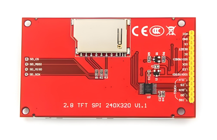
                        • Electrolytic Tough Pitch (ETP) Copper: This is the standard. It’s over 99% pure and offers great conductivity and flexibility.
                        • Rolled Annealed (RA) Copper: This type is used in flexible PCBs. It’s softer, more bendable, and less likely to crack under repeated movement.

                        For rigid boards, like your TV remote or thermostat, ETP is ideal. For flexible applications, like foldable phones or wearable devices, RA copper shines.

                        How to choose PCB copper thickness?

                        Picking the right copper PCB board thickness depends on your needs. Here are some guiding points:

                        • Current load: More current needs thicker copper. If your board handles power, go for 2 oz or more.
                        • Heat management: Thicker copper spreads heat better, reducing hotspots.
                        • Space constraints: If your design is tight, thinner copper can help save room.
                        • Cost and weight: More copper = more weight and higher cost.

                        The most common thickness is 1 oz, but 0.5 oz and 2 oz are also widely used. High-power boards may go up to 3 oz or more.

                        What is a copper clad PCB board?

                        Copper clad PCB board is a base material, Usually FR4 (fiberglass), CEM-1, or phenolic resin, that’s laminated with a thin layer of copper on one or both sides.

                        Types of copper clad boards include:

                        • Single sided copper clad board: copper on one side
                        • Double sided copper clad board: copper on both sides
                        • Multilayer boards: multiple layers of copper and insulation stacked together

                        These boards form the foundation of electronics. Without copper cladding, there’s no signal path, no connectivity, and no functionality.

                        Types of Copper Clad Boards

                        There are several variations, each tailored for different needs:

                        • Single sided copper PCB board: Great for simple, low-cost circuits. Common in calculators or basic toys.
                        • Double sided copper PCB board: Used in more complex electronics, offering better routing and signal flow.
                        • Copper clad laminate: This is the raw material, often sold in panels, ready to be etched. Also known as blank copper PCB board.
                        • Double sided copper clad laminate PCB circuit board: Offers flexibility in circuit design. Common in LED lighting and power supplies.
                        • Copper strip PCB board: Used for high-current circuits. Thick copper strips are embedded to carry heavy loads.
                        • Copper clad plate laminate PCB board: Known for high strength, used in industrial environments.

                        The choice depends on application, current needs, size, and cost.

                        What is a copper clad board used for?

                        Copper clad boards are used in every corner of the electronics world.

                        • Consumer electronics
                        • Industrial controls
                        • LED lighting
                        • Automotive dashboards
                        • Medical devices
                        • Communication systems

                        Their job? To carry signals, distribute power, and provide mechanical support. They’re also vital for EMI shielding, grounding, and signal integrity.

                        How to remove copper from PCB board?

                        There are moments in prototyping or repair when removing copper is necessary. Here are some common methods:

                        • Chemical etching: Ferric chloride or ammonium persulfate can dissolve copper. Be cautious, it’s toxic and requires proper ventilation.
                        • Mechanical removal: Sandpaper or a rotary tool can physically grind off copper.
                        • Laser removal: High-end labs use this for ultra-precise control.

                        Each method has pros and cons. For hobbyists, mechanical methods are safer. For professionals, chemical etching allows for mass removal with precision.

                        Copper plated PCB board vs copper coated: What’s the difference?

                        Copper plated PCB boards and copper coated PCB boards may sound similar, but they serve different purposes.

                        Copper plated PCB board means copper has been electroplated onto certain areas—like holes or edges. This helps with conductivity, especially in via holes and multi-layer connections.

                        Copper coated PCB board refers to a board where a base material is uniformly covered with copper foil. This is typically done during the lamination stage to form the initial circuit layer.

                        In short:

                        • Plated = targeted copper application, used for conductivity enhancement
                        • Coated = general copper layer across a surface, used to form the main circuit

                        Conclusion:

                        Copper PCB boards play a critical role in modern electronics, offering excellent conductivity, thermal performance, and reliability. Whether it’s a single sided copper clad board, double sided copper PCB board, or a blank copper PCB board, each type supports different circuit needs.

                        If you’re looking for high-quality copper clad PCB boards, reliable support, or expert advice, we’re here to help.

                        Need help choosing the right copper PCB board? Reach out today at sales@bestpcbs.com

                        You may also like